News Posts matching #10 nm

Return to Keyword Browsing

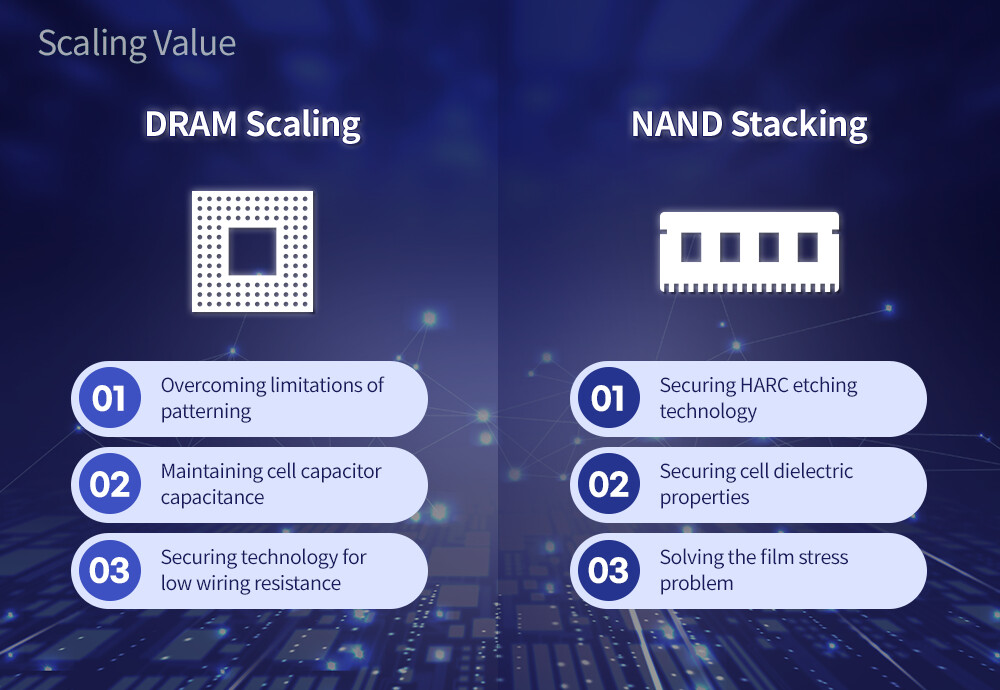
Intel to Outsource a Part of 2023 Processor Production to TSMC

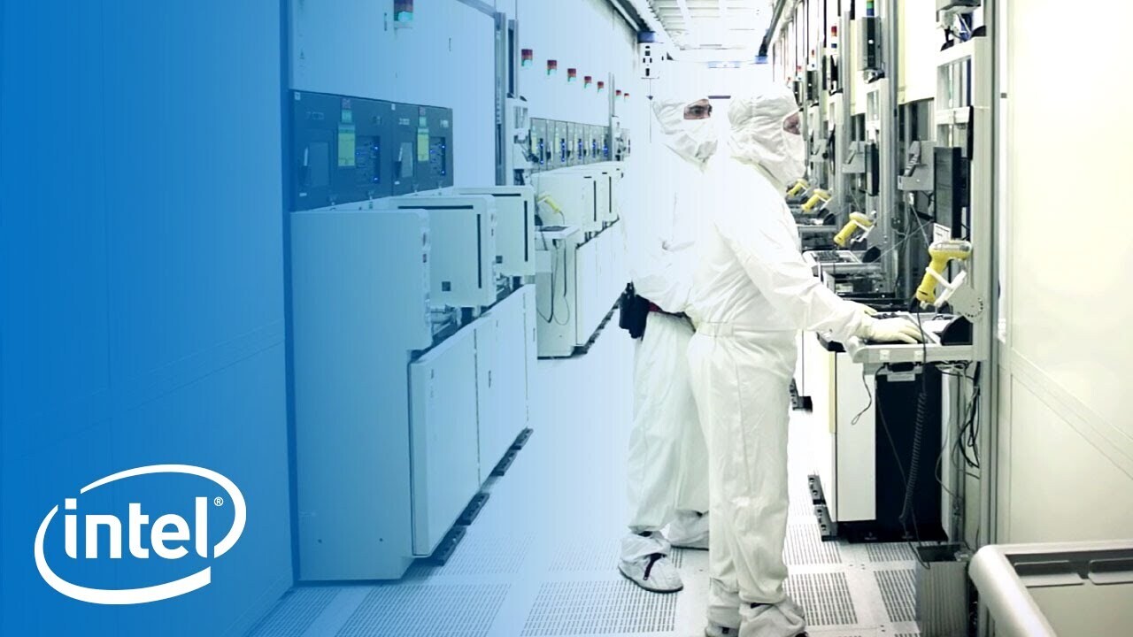
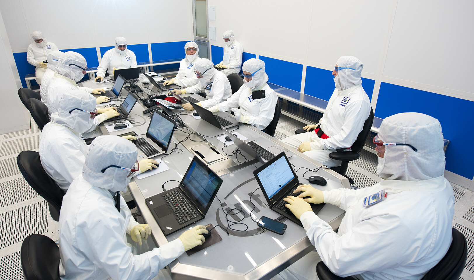
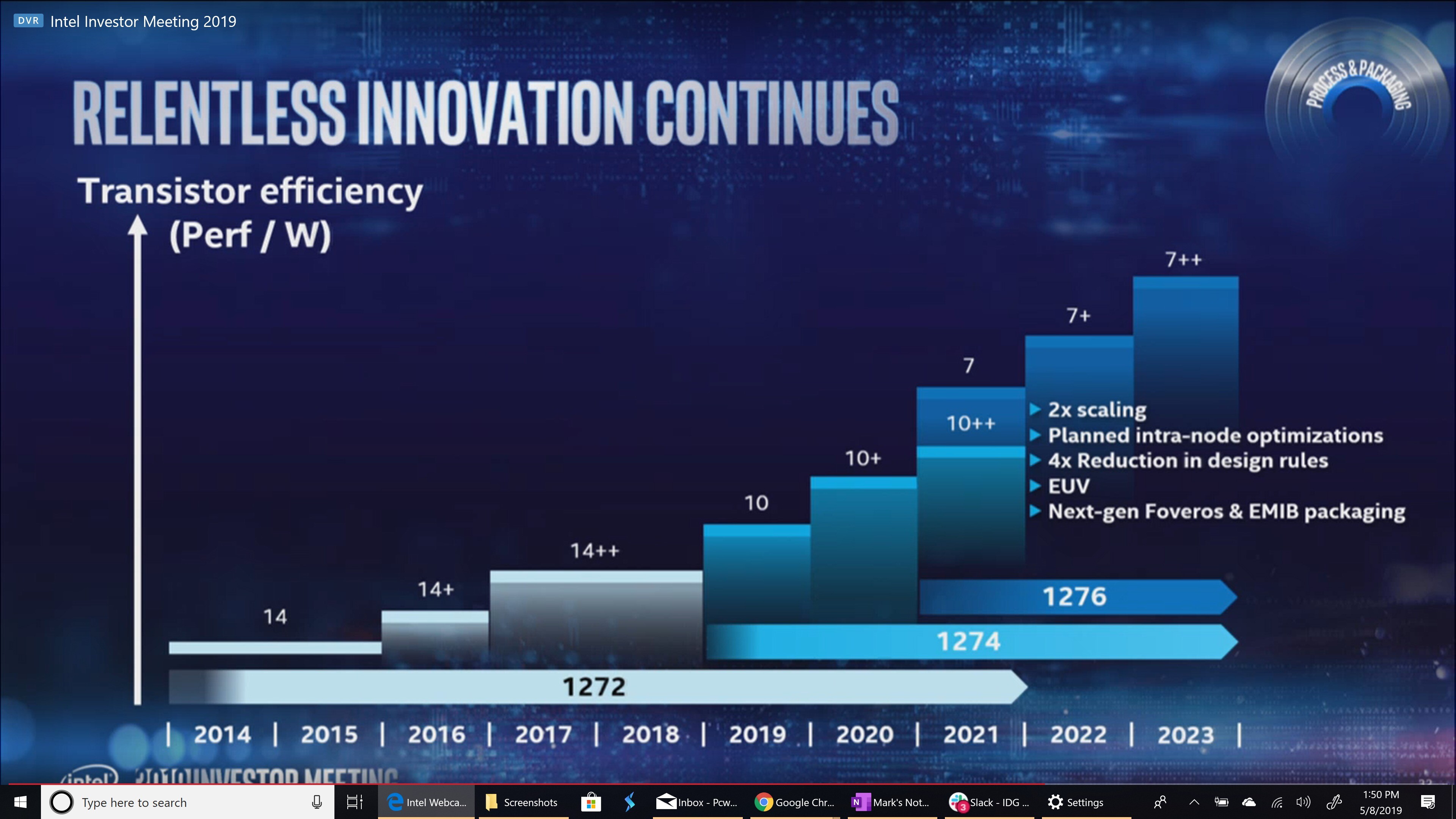
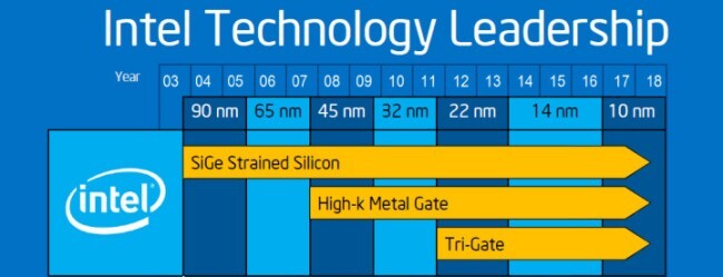
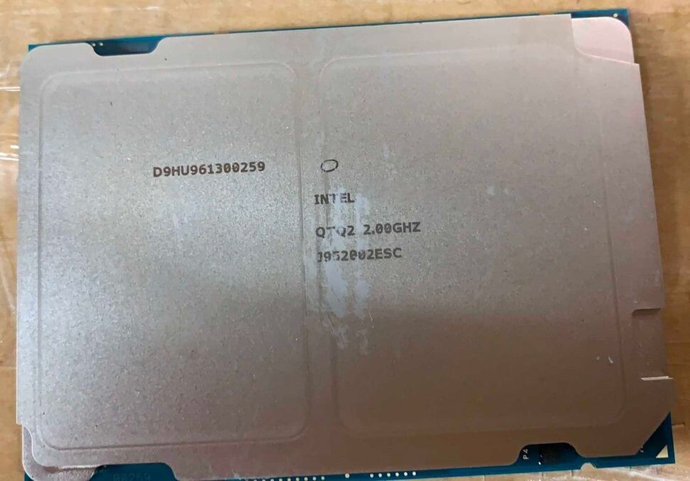
Intel's problems with processor production, especially with newer nodes like 10 nm and 7 nm, have been widely known. The company has not been able to deliver the latest semiconductor process on time and has thus delayed many product launches. However, things are looking to take a complete U-turn and the hell will freeze. During the "Intel Unleashed: Engineering the Future" webcast event that happened yesterday, the company made several announcements regarding the 7 nm process and its viability. We have already reported that the company is working on the new Meteor Lake processor lineup for 2023, supposed to be manufactured on the fixed 7 nm node.

However, it seems like Intel will have to tap external capacities to manufacture a part of its processor production. The company has confirmed that it will use an unknown TSMC process to manufacture a part of the 2023 processor lineup. That means that Intel and TSMC have already established the needed capacity and that TSMC has already booked wafer capacity for Intel. This has never happened before, as Intel always kept its processor production under the company roof. However, given that there is a huge demand for new semiconductor processes, Intel has to look at external manufacturing options to keep up with the demand.

SK Hynix Envisions the Future: 600-Layer 3D NAND and EUV-made DRAM

On March 22nd, the CEO of SK Hynix, Seok-Hee Lee, gave a keynote speech to the IEEE International Reliability Physics Symposium (IRPS) and shared with experts a part of its plan for the future of SK Hynix products. The CEO took the stage and delivered some conceptual technologies that the company is working on right now. At the center of the show, two distinct products stood out - 3D NAND and DRAM. So far, the company has believed that its 3D NAND scaling was very limited and that it can push up to 500 layers sometime in the future before the limit is reached. However, according to the latest research, SK Hynix will be able to produce 600-layer 3D NAND technology in the distant future.

So far, the company has managed to manufacture and sample 512Gb 176-layer 3D NAND chips, so the 600-layer solutions are still far away. Nonetheless, it is a possibility that we are looking at. Before we reach that layer number, there are various problems needed to be solved so the technology can work. According to SK Hynix, "the company introduced the atomic layer deposition (ALD) technology to further improve the cell property of efficiently storing electric charges and exporting them when needed, while developing technology to maintain uniform electric charges over a certain amount through the innovation of dielectric materials. In addition to this, to solve film stress issues, the mechanical stress levels of films is controlled and the cell oxide-nitride (ON) material is being optimized. To deal with the interference phenomenon between cells and charge loss that occur when more cells are stacked at a limited height, SK Hynix developed the isolated-charge trap nitride (isolated-CTN) structure to enhance reliability."

Intel to Launch 3rd Gen Intel Xeon Scalable Portfolio on April 6

Intel today revealed that it will launch its 3rd Generation Xeon Scalable processor series at an online event titled "How Wonderful Gets Done 2021," on April 6, 2021. This will be one of the first major media events headed by Intel's new CEO, Pat Gelsinger. Besides the processor launch, Intel is expected to detail many of its advances in the enterprise space, particularly in the areas of 5G infrastructure rollout, edge computing, and AI/HPC. The 3rd Gen Xeon Scalable processors are based on the new 10 nm "Ice Lake-SP" silicon, heralding the company's first CPU core IPC gain in the server space since 2015. The processors also introduce new I/O capabilities, such as PCI-Express 4.0.

Intel 12th Generation Alder Lake Platform Reportedly Brings 20% Single-Threaded Performance Uplift

Intel only just announced their 11th generation Rocket Lake-S desktop processors last week but we are already receiving information about the next generation Alder Lake-S platform which will finally make the jump to 10 nm. Intel slides for the upcoming family of processors have been leaked and they reveal some interesting information including a claimed 20% single-threaded performance increases from the new Golden Cove core design and 10 nm SuperFin node. The processors will feature Intel Hybrid Technology with a mix of small low-performance cores and large high-performance cores with a maximum of eight each for sixteen total cores. The processors will also include the latest connectivity with both PCIe 4.0 and PCIe 5.0 support along with DDR4 and DDR5 4800 MHz compatibility.

Intel will also be launching a new socket type called LGA1700 with a new package size which will render existing cooling solutions for LGA115X and LGA1200 sockets incompatible. The processors will also come with the launch of a new 600 Series chipset with PCIe 3.0 and PCIe 4.0 support along with the usual complement of USB, SATA, and networking. The entry-level 600-series motherboards will only support DDR4 memory at up to 3200 MHz while high-end Z690 motherboards will include DDR5 support. Intel has confirmed that they intend to launch Alder Lake later this year but it is yet to be known if they are referring to the desktop or mobile series.

HPE Lists 40-Core Intel Ice Lake-SP Xeon Server Processor

Hewlett Packard Enterprise, the company focused on making enterprise hardware and software, has today mistakenly listed some of Intel's upcoming 3rd generation Xeon Scalable processors. Called Ice Lake-SP, the latest server processor generation is expected to launch sometime in the coming days, with a possible launch date being the March 23rd "Intel Unleashed" webcast. The next generation of processors will finally bring a new vector of technologies Intel needs in server space. That means the support for PCIe 4.0 protocol for higher speed I/O and octa-channel DDR4 memory controller for much greater bandwidth. The CPU lineup will for the first time use Intel's advanced 10 nm node called 10 nm SuperFin.

Today, in the leaked HPE listing, we get to see some of the Xeon models Intel plans to launch. Starting from 32-core models, all the way to 40-core models, all SKUs above 28 cores are supposed to use dual die configuration to achieve high core counts. The limit of a single die is 28 cores. HPE listed a few models, with the highest-end one being the Intel Xeon Platinum XCC 8380 processor. It features 40 cores with 80 threads and a running frequency of 2.3 GHz. If you are wondering about TDP, it looks like the 10 nm SuperFin process is giving good results, as the CPU is rated only for 270 Watts of power.

Intel and DARPA Develop Secure Structured ASIC Chips Made in the US

Intel and the U.S. Defense Advanced Research Projects Agency (DARPA) today announced a three-year partnership to advance the development of domestically manufactured structured Application Specific Integrated Circuit (ASIC) platforms. The Structured Array Hardware for Automatically Realized Applications (SAHARA) partnership enables the design of custom chips that include state-of-the-art security countermeasure technologies. A reliable, secure, domestic source of leading-edge semiconductors remains critical to the U.S.

"We are combining our most advanced Intel eASIC structured ASIC technology with state-of-the-art data interface chiplets and enhanced security protection, and it's all being made within the U.S. from beginning to end. This will enable defense and commercial electronics systems developers to rapidly develop and deploy custom chips based on Intel's advanced 10 nm semiconductor process," said José Roberto Alvarez, senior director, CTO Office, Intel Programmable Solutions Group.

Intel to Unveil "Tiger Lake-H" and "Rocket Lake-S" on March 18

Intel is expected to unveil its 11th generation Core "Tiger Lake-H" performance-segment mobile processor, and the highly anticipated 11th Gen Core "Rocket Lake-S" desktop processor family on March 18, 2021. The two will be launched on the sidelines of the 2021 GDC (Game Developers Conference), an online event. The agenda page of GDC mentions both "Tiger Lake-H" and "Rocket Lake." The "Tiger Lake-H" family of processors begin with quad-core SKUs based on the 4-core "Tiger Lake" silicon, extending to 6-core and 8-core ones based on a newer 8-core silicon. Both dies are built on the 10 nm SuperFin node, and combine Intel's highest-IPC "Willow Cove" CPU cores with a Gen 12 Xe iGPU.

The 11th Gen Core "Rocket Lake-S" has been unveiled back at the 2021 International CES (online event) in January, and is heading toward a mid/late-March launch. The chips pack up to eight "Cypress Cove" CPU cores, which are a back-port of Intel's 10 nm CPU core architectures to the 14 nm node, bringing the first IPC increase on the client desktop platform from Intel since 2015. At GDC, we expect Intel to detail individual SKUs within the 11th Gen Core processor family, giving us a broader idea of what chips will launch this month. The GDC backdrop also foreshadows the marketing strategy for Intel with both these platforms—gaming. The company will take advantage of the IPC uplift to present its processors as being better for gaming, and sufficiently fast in most client-relevant tasks. The GDC backdrop could also let Intel show off the ISV relations it's built with game developers, detailing how certain popular game engines are optimized for Intel.

Durabook Unveils All-New S14I Laptop With Advanced Computing Power

Durabook, the global rugged mobile solutions brand owned by Twinhead International Corporation, announced today that it is taking rugged computing performance to new heights with its all-new S14I 14-inch semi-rugged laptop. The S14I laptop pushes the boundaries of semi-rugged design and innovation to deliver ultimate mobile computing experiences. The new generation S14I will be available in April and includes the following upgrades: the new Intel Tiger Lake 11th generation processors, the latest NVMe PCIe SSD solution and the Intel Iris Xe MAX graphics or the option of NVIDIA GeForce GTX 1050 discrete graphics.

"Our refreshed S14I laptop takes semi-rugged devices to a whole new level," stated Tom Wang, Durabook Americas president. "This advanced version further enhances the unit's perfect combination of military-grade durability, certified with IP53 and 4-foot drop, field-worker functionality, computer performance, and long battery life of 12 hours. It is the perfect mobile device for today's demanding and diverse working environments with its DynaVue sunlight-readable technology. There is no wonder why the Durabook S14I is the most rugged laptop in its class."

Intel Plans a Sizable 11th Gen Core "Tiger Lake-H" Mobile Processor Lineup

Intel's new 8-core "Tiger Lake" silicon will play a major role in holding the company's dominance in the mobile processor space, with plans for new 6-core and 8-core SKUs being in motion. OneRaichu on Twitter, a reliable source with Intel leaks, points to several unreleased model numbers. The 8-core "Tiger Lake-H" die is expected to be built on the same 10 nm SuperFin process as the "Tiger Lake-U" silicon. The lineup is led by the Core i9-11980HK, an 8-core/16-thread processor that uses eight "Willow Cove" CPU cores, 2.60 GHz nominal- and 5.00 GHz max-Turbo frequency, and 3.30 GHz AVX512 frequency. This chip will be in a class of its own, as its TDP is rated at 65 W, significantly above the 35-45 W TDP range that constitutes the H-segment. It will likely power large gaming notebooks with elaborate cooling solutions. It will also come with an unlocked base-clock multiplier.

The Core i9-11900H is the next chip in the lineup, with slightly lower clock speeds of 2.50 GHz base, 4.90 GHz max-Turbo, and 2.10 GHz AVX512. This chip features a much lower 35 W TDP, and will come with aggressive power management compared to the i9-11980HK. The Core i7-11800H will be the slowest 8-core part, with clock speeds of 2.40 GHz nominal, 4.60 GHz max-Turbo, and 2.00 GHz AVX512. It comes with the same 35 W TDP as the i9-11900H. Next up, are 6-core/12-thread parts, likely under the Core i5 brand. These include the i5-11400H, clocked at 2.70 GHz nominal, 4.50 GHz max-Turbo, and 2.20 GHz AVX512. At the bottom of the pile is the i5-11260H, clocked at 2.60 GHz, with 4.40 GHz max-Turbo, and 2.10 GHz AVX512. Both Core i5 parts are 35-Watt.

Intel Rocket Lake-S Lands on March 15th, Alder Lake-S Uses Enhanced 10 nm SuperFin Process

In the latest round of rumors, we have today received some really interesting news regarding Intel's upcoming lineup of desktop processors. Thanks to HKEPC media, we have information about the launch date of Intel's Rocket Lake-S processor lineup and Alder Lake-S details. Starting with Rocket Lake, Intel did not unveil the exact availability date on these processors. However, thanks to HKEPC, we have information that Rocket Lake is landing in our hands on March 15th. With 500 series chipsets already launched, consumers are now waiting for the processors to arrive as well, so they can pair their new PCIe 4.0 NVMe SSDs with the latest processor generation.

When it comes to the next generation Alder Lake-S design, Intel is reported to use its enhanced 10 nm SuperFin process for the manufacturing of these processors. This would mean that the node is more efficient than the regular 10 nm SuperFin present on Tiger Lake processors, and some improvements like better frequencies are expected. Alder Lake is expected to make use of big.LITTLE core configuration, with small cores being Gracemont designs, and the big cores being Golden Cove designs. The magic of Golden Cove is expected to result in 20% IPC improvement over Willow Cove, which exists today in Tiger Lake designs. Paired with PCIe 5.0 and DDR5 technology, Alder Lake is looking like a compelling upgrade that is arriving in December of this year. Pictured below is the LGA1700 engineering sample of Alder Lake-S processor.

Intel Xe DG1 SDV PCB Pictured, Looks Desolate

Here are some of the first pictures of the Intel Xe DG1 SDV, taken apart to reveal its rather desolate PCB. The Xe DG1 SDV isn't commercially available, but rather distributed by Intel to ISVs, so they can begin optimizing or developing for the Gen12 Xe graphics architecture. The board features a GPU ASIC that's nearly identical to the Iris Xe MAX mobile discrete GPUs, and four LPDDR4 memory chips making up 8 GB of video memory.

The Xe DG1 GPU is based on the Xe LP graphics architecture, and the silicon is built on the 10 nm SuperFin silicon fabrication node. The chip features 96 execution units (768 unified shaders); and apparently makes do with the 75 W power supplied by the PCI-Express slot. A frugal 2-phase VRM powers the GPU. The GPU uses conventional 4-pin PWM to control the fan, which ventilates a simple aluminium mono-block heatsink. Three DisplayPorts and one HDMI 2.1 make up the output configuration. While you won't be able to buy a Xe DG1 SDV in the market (unless an ISV decides to break their NDA and put one up on eBay), Intel has allowed a small number of board partners to develop custom-design cards. ASUS is ready with one. Igor's Lab has more pictures, a list of benchmark fails, and other interesting commentary in the source link below.

Intel "Alder Lake-S" Due for September 2021

2021 is shaping up to be a big year for Intel in the DIY desktop space, with the company preparing to launch not one, but two generations of desktop processors. Having announced them in January, the 11th Gen Core "Rocket Lake-S" desktop processors in the LGA1200 package, will release to market in March, with the company claiming a restoration in gaming performance leadership away from AMD's Ryzen 5000 series. Sources tell Uniko's Hardware that the company will announce its 12th Gen successor, the Core "Alder Lake-S" in September 2021.

"Alder Lake-S" will be Intel's first mainstream desktop processor built on its new 10 nm SuperFin silicon fabrication process. The chip is expected to be a "hybrid" processor, combining an equal number of larger "Golden Cove" cores, and smaller "Gracemont" cores, to offer significantly improved energy efficiency. Built in the new Socket LGA1700 package, "Alder Lake-S" is expected to feature more general-purpose SoC connectivity than LGA1200 chips. It will also herald new platform standards, such as DDR5 memory and possibly even mainstreaming of ATX12VO. The processor will launch alongside new Intel 600-series chipset. AMD's response is expected to be the "Zen 4" microarchitecture, a new silicon built on the 5 nm process, and the new AM5 socket that introduces DDR5 memory support.

Intel Has Fixed its 7 nm Node, But Outsourcing is Still Going to Happen

Intel has today reported its Q4 2020 earnings disclosing full-year revenue with the current CEO Bob Swan, upcoming new CEO Pat Gelsinger, and Omar Ishrak, Chairman of Intel's board. During the call, company officials have talked about Intel's earnings and most importantly, addressing the current problems about the company's manufacturing part - semiconductor foundries. Incoming Intel CEO, Pat Gelsinger, has talked about the state of the 7 nm node, giving shareholders reassurance and a will to remain in such a position. He has made an argument that he has personally reviewed the progress of the "health and recovery of the 7 nm program."

The 7 nm node has been originally delayed by a full year amid the expectations, and as with the 10 nm node, we have believed that it is going to experience similar issues. However, the incoming CEO has reassured everyone that it is very much improving. The new 7 nm node is on track for 2023 delivery, when Intel is expected to compete with the 3 nm node of TSMC. Firstly, Intel will make a debut of the 7 nm node with client processors scheduled for 1H 2023 arrival, with data center models following that. The company leads have confirmed that Intel will stay true to its internal manufacturing, but have stressed that there will still be a need for some outsourcing to happen.

Intel Starts Production of "Ice Lake" Xeons, Ships 11th Gen Core "Rocket Lake-S"

Intel in its FY 2020 + Q4 2020 earnings release revealed two important development milestones from its two core businesses. As part of its Q4 2020 business highlights disclosures, the company revealed that it has commenced mass-production of its next-generation Xeon Scalable "Ice Lake-SP" enterprise processors. These chips implement the "Ice Lake" microarchitecture, with "Sunny Cove" CPU cores that offer higher IPC over "Cascade Lake," and are built on the company's 10 nm silicon fabrication node. Our older article details the 10 nm "Ice Lake-SP" silicon, where each die offers up to 28 cores, and enables Intel to build processors with up to 56 cores using two such dies on multi-chip modules.

Next up, the company states that it has "started shipping" its 11th Gen Core "Rocket Lake-S" desktop processors. "Shipping" in this context could even mean commencement of mass-production, and transfer of inventory down the supply chain, in the build up to a market availability date. At its digital keynote address on the sidelines of the 2021 International CES, Intel revealed many more details of "Rocket Lake-S," including its flagship Core i9-11900K 8-core processor, which it claims retakes the gaming performance lead that the company recently lost to AMD's Ryzen 5000 series. Multiple sources confirmed that these processors should be available only after mid-March, 2021.

Intel Reports Fourth-Quarter and Full-Year 2020 Financial Results

Intel Corporation today reported fourth-quarter and full-year 2020 financial results. The company also announced that its board of directors approved a cash dividend increase of five percent to $1.39 per share on an annual basis. The board declared a quarterly dividend of $0.3475 per share on the company's common stock, which will be payable on March 1 to shareholders of record on February 7.

"We significantly exceeded our expectations for the quarter, capping off our fifth consecutive record year," said Bob Swan, Intel CEO. "Demand for the computing performance Intel delivers remains very strong and our focus on growth opportunities is paying off. It has been an honor to lead this wonderful company, and I am proud of what we have achieved as a team. Intel is in a strong strategic and financial position as we make this leadership transition and take Intel to the next level."

16-Core Intel Alder Lake-S Processor Appears with DDR5 Memory

Intel has just launched its Rocket Lake-S desktop lineup of processors during this year's CES 2021 virtual event. However, the company is under constant pressure from the competition and it seems like it will not stop with that launch for this year. Today, thanks to the popular leaker @momomo_us on Twitter, we have the first SiSoftware entries made from the anonymous Alder Lake-S system. Dubbed a heterogeneous architecture, Alder Lake is supposed to be Intel's first desktop attempt at making big.LITTLE style of processors for general consumers. It is supposed to feature Intel 10 nm Golden Cove CPU "big" cores & Gracemont "small" CPU cores.

The SiSoftware database entry showcases a prototype system that has 16 cores and 32 threads running at the base frequency of 1.8 GHz and a boost speed of 4 GHz. There is 12.5 MB of L2 cache (split into 10 pairs of 1.25 MB) and 30 MB of level-three (L3) cache present on the processor. There is also an Alder Lake-S mobile graphics controller that runs at 1.5 GHz. Intel Xe gen 12.2 graphics is responsible for the video output. When it comes to memory, Alder Lake-S is finally bringing the newest DDR5 standard with a new motherboard chipset and socket called LGA 1700.

Intel Starts Production of 10nm Xeon Scalable Processors

Intel highlighted the company's focus on execution of core products and showcased the company's broader portfolio, in addition to sharing more on what's coming in the year ahead. As part of its disclosures, Intel announced the recent production of its 3rd Gen Intel Xeon Scalable processors (code-named "Ice Lake") with volume ramp taking place during the first quarter of 2021. Intel's 10 nm Xeon Scalable processors feature architectural and platform innovations that boost performance, security and operational efficiency within data centers.

"Today marks a significant milestone for Intel as we continue to accelerate the delivery of our 10 nm products and maintain an intense focus on delivering a predictable cadence of leadership products for our customers," said Navin Shenoy, executive vice president and general manager of the Data Platforms Group at Intel. "Our 3rd Gen Intel Xeon Scalable platform represents a strategic part of our data center strategy and one that we've created alongside some of our biggest customers to enable the data center of tomorrow."

Intel CEO Says Using Competitor's Semiconductor Process in Intel Fabs is an Option

Semiconductor manufacturing is not an easy feat to achieve. Especially if you are constantly chasing the smaller and smaller node. Intel knows this the best. The company has had a smooth transition from other nodes to the smaller ones until the 10 nm node came up. It has brought Intel years of additional delay and tons of cost improving the yields of a node that was seeming broken. Yesterday the company announced the new Tiger Lake-H processors for laptops that are built using the 10 nm process, however, we are questioning whatever Intel can keep up with the semiconductor industry and deliver the newest nodes on time, and with ease. During an interview with Intel's CEO Bob Swan, we can get a glimpse of Intel's plans for the future of semiconductors at the company.

In the interview, Mr. Swan has spoken about the technical side of Intel and how the company plans to utilize its Fabs. The first question everyone was wondering was about the state of 10 nm. The node is doing well as three Fabs are ramping up capacity every day, and more products are expected to arrive on that node. Mr. Swan has also talked about outsourcing chip production, to which he responded by outlining the advantage Intel has with its Fabs. He said that outsourcing is what is giving us shortages like AMD and NVIDIA experience, and Intel had much less problems. Additionally, Mr. Swan was asked about the feasibility of new node development. To that, he responded that there is a possibility that Intel could license its competitor's node and produce it in their Fabs.

Intel Announces Four New Processor Families

In a world where computing is pervasive and intelligence is distributed across every surface - from the cloud to the network to the intelligent edge - Intel today at CES 2021 highlighted how it is driving technology leadership to define the future of computing for people, business and society. To help people navigate through this extraordinary time, Intel introduced new processors for business, education, mobile and gaming computing platforms - all designed to offer the premium PC experiences people deserve, with the most choices and no limits.

"Only Intel has the breadth of products spanning multiple architectures; the large, open ecosystem; sheer scale of manufacturing footprint; and deep technical expertise customers need to unlock opportunities in this era of distributed intelligence," said Intel Executive Vice President Gregory Bryant. "With an intense focus on execution for our core products and across our broader portfolio, we're introducing a series of leadership products at CES with more following throughout the year."

Hedge Fund Urges Intel to Outsource Chip Production: Reuters

Intel is familiar with chip manufacturing problems since the company started the development of a 10 nm silicon semiconductor node. The latest node is coming years late with many IPs getting held back thanks to the inability of the company to produce it. All of Intel's chip production was historically happening at Intel's facilities, however, given the fact that the demand for 14 nm products is exceeding production capability, the company was forced to turn to external foundries like TSMC to compensate for its lack of capacity. TSMC has a contract with Intel to produce silicon for things like chipsets, which is offloading a lot of capacity for the company. Today, thanks to the exclusive information obtained by Reuters, we have information that a certain New York hedge fund, Third Point LLC, is advising the company about the future of its manufacturing.

The hedge fund is reportedly accounting for about one billion USD worth of assets in Intel, thus making it a huge and one influencing shareholder. The Third Point Chief Executive Daniel Loeb wrote a letter to Intel Chairman Omar Ishrak to take immediate action to boost the company's state as a major provider of processors for PCs and data centers. The company has noted that Intel needs to outsource more of its chip production to satisfy the market needs, so it can stay competitive with the industry. The poor performance of Intel has reflected on the company shares, which have declined about 21% this year. This has awoken the shareholders and now we see that they are demanding more aggressiveness from the company and a plan to outsource more of the chip production to partner foundries like TSMC and Samsung. It remains to be seen how Intel responds and what changes are to take place.

Intel Expands 10nm Manufacturing Capacity

In response to incredible customer demand, Intel has doubled its combined 14 nm and 10 nm manufacturing capacity over the past few years. To do this, the company found innovative ways to deliver more output within existing capacity through yield improvement projects and significant investments in capacity expansion. This video recounts that journey, which even included re-purposing existing lab and office space for manufacturing.

"Over the last three years, we have doubled our wafer volume capacity, and that was a significant investment. Moving forward, we're not stopping… We are continuing to invest into factory capacity to ensure we can keep up with the growing needs of our customers," says Keyvan Esfarjani, senior vice president and general manager of Manufacturing and Operations at Intel. The company also ramped its new 10 nm process this year. Intel currently manufactures 10 nm products in high volumes at its Oregon and Arizona sites in the U.S. and its site in Israel.

Intel's Manufacturing Outlook for the Future Doesn't Inspire Confidence in Successful Competition, According to Susquehanna Call

Susquehanna is a global trading firm which has various interests in silicon manufacturing - and part of that interest is naturally materialized in Intel. In a recent group call from the firm, some details on Intel's manufacturing and product design woes came to light, which point towards even more execution slips than we've already seen. During the call, a number of points were broached, including dismal yields for Intel's 10 nm manufacturing process as of its introduction in late 2018 (which is why it never saw mainstream adoption from the company). News that Intel is looking for a new CEO also don't instill confidence on current CEO Bob Swan's capacity to steer the Intel behemoth.

Improved yields on 10 nm are being reported due to deployment of Intel's SuperFin technology, which improved yields to upwards of 50%, but still keeps them under the ones achieved in Intel's 14 nm process; an eye-opening tidbit in that Cannon Lake on 10 nm originally saw yields of only 25% usable chips per wafer; and that backporting Rocket Lake meant Intel had to deal with unfathomably large chips and high power consumption characteristics. And to add insult to injury, there is still not a definite timetable for 7 nm deployment, with delays being expected to be worse than the previously reported 6-12 months. This all paints a somewhat grim picture for Intel's capacity to compete with TSMC-powered AMD in many of its most important markets; the blue giant won't topple, of course, but it's expected that five years from now, we'll be looking at a very different outlook in the market between AMD and Intel. You can check the talked-about points in the call via the transcript after the break. You should still take the transcript with a grain of salt.

Alleged Intel Sapphire Rapids Xeon Processor Image Leaks, Dual-Die Madness Showcased

Today, thanks to the ServeTheHome forum member "111alan", we have the first pictures of the alleged Intel Sapphire Rapids Xeon processor. Pictured is what appears to be a dual-die design similar to Cascade Lake-SP design with 56 cores and 112 threads that uses two dies. The Sapphire Rapids is a 10 nm SuperFin design that allegedly comes even in the dual-die configuration. To host this processor, the motherboard needs an LGA4677 socket with 4677 pins present. The new LGA socket, along with the new 10 nm Sapphire Rapids Xeon processors are set for delivery in 2021 when Intel is expected to launch its new processors and their respective platforms.

The processor pictured is clearly a dual-die design, meaning that Intel used some of its Multi-Chip Package (MCM) technology that uses EMIB to interconnect the silicon using an active interposer. As a reminder, the new 10 nm Sapphire Rapids platform is supposed to bring many new features like a DDR5 memory controller paired with Intel's Data Streaming Accelerator (DSA); a brand new PCIe 5.0 standard protocol with a 32 GT/s data transfer rate, and a CXL 1.1 support for next-generation accelerators. The exact configuration of this processor is unknown, however, it is an engineering sample with a clock frequency of a modest 2.0 GHz.

Intel Ice Lake-SP Processor Spotted with 36 Cores and 3.6 GHz Base Clock

Today, in the latest GeekBench 5 submission by ASUS, we have discovered something rather interesting. Intel's Ice Lake-SP processors were rumored to arrive with up to 28 cores and 56 threads at maximum, on a single chip. That was due to the 10 nm process used to make these chips, with suspicions that the yield of the node was not good enough to make any higher core count parts. Thanks to the GB5 listing, discovered by Leakbench on Twitter, the Intel Ice Lake-SP CPU engineering sample appeared with an amazing 36 cores with 72 threads. This is supposedly Intel's efforts to try and match the 64 cores and 128 threads of AMD's EPYC "Rome" CPUs, which are winning many server applications due to their performance.

The 36C/72T chip was paired with another similar chip in a 2P dual-socket configuration, which made the total core count rise to 72 cores and 144 threads, running inside of Asustek's Y4R-A1-ASUS-G1 server. The system was reporting a clock frequency of 3.6 GHz base speed, which means that the possible boost clocks could be higher. The CPU features a 1.25 MB level two (L2) cache per core (45 MB in total) and 54 MB of unified level three (L3) cache. That makes this CPU core quite an improvement over the past Cooper Lake generation. We are waiting for more information about these CPUs, and we are going to report on it in the coming time.

Intel 11th Generation Core Tiger Lake-H Processor Appears

Intel has launched its Tiger Lake-U lineup of products back in September, with the availability of the first products in October. The launched lineup was part of the "U" variant of ultra-portable devices that stretched only to four core, eight threaded configurations. However, given that the new competitor in mobile space, AMD, has a wide portfolio of offerings that are coming with up to 8C/16T variants, Intel needs a proper response to that. Despite having a better single-threaded performance, the multi-threaded capability of the Ryzen 4000 series is delivering better performance. Thanks to the popular hardware leaker, TUM APISAK, we have the first appearance of Intel's 11th generation Tiger Lake-H processor.

Appearing in Userbenchmark, the processor was tested on a platform codenamed "Insyde TigerLake". The processor was spotted running 8 cores and 16 threads, at the average frequency of 2.75 GHz. This is only an engineering sample, meaning that these clocks do not represent the final frequencies of the processor. As a reminder, Intel's Tiger Lake CPU is a Willow Cove based design manufactured on Intel's 10 nm SuperFin silicon node. We are yet to see the capabilities of the new node and how the chip performs once the reviews arrive.
Return to Keyword Browsing
May 15th, 2024 18:04 EDT change timezone

New Forum Posts

Popular Reviews

Controversial News Posts