News Posts matching #12 nm

Return to Keyword Browsing

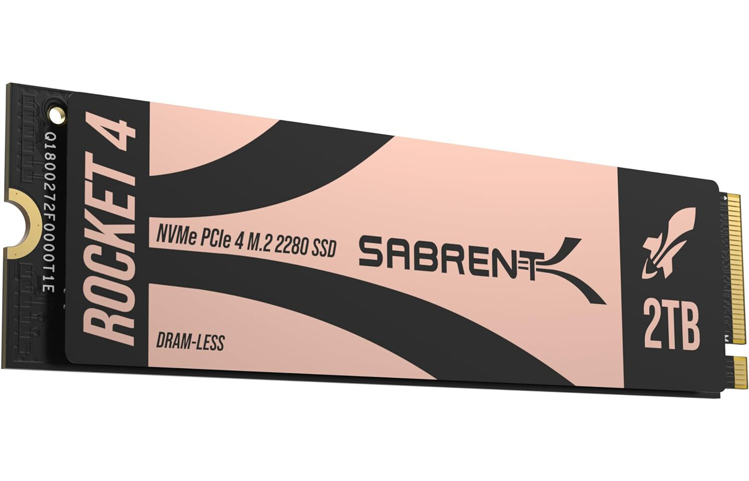
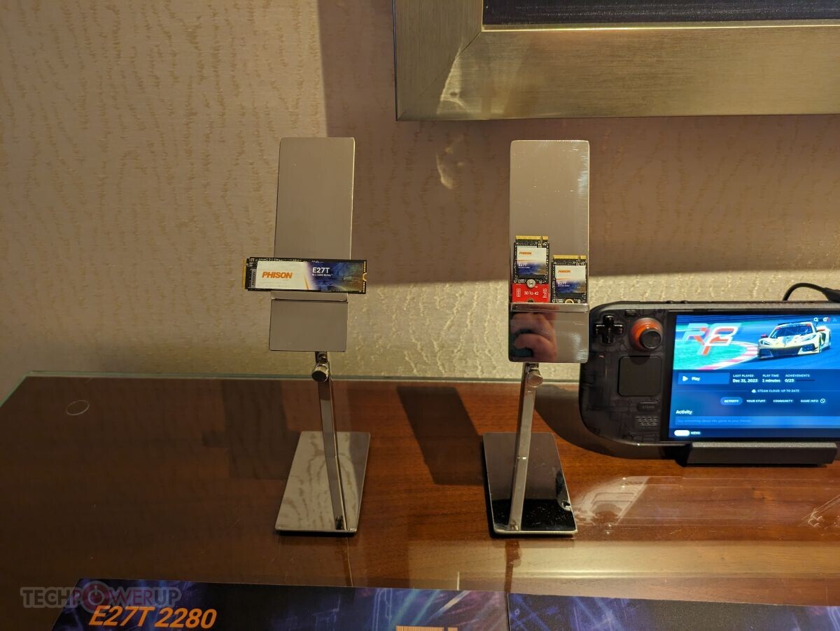
Sabrent Announces the Rocket 4 DRAMless M.2 Gen 4 SSD

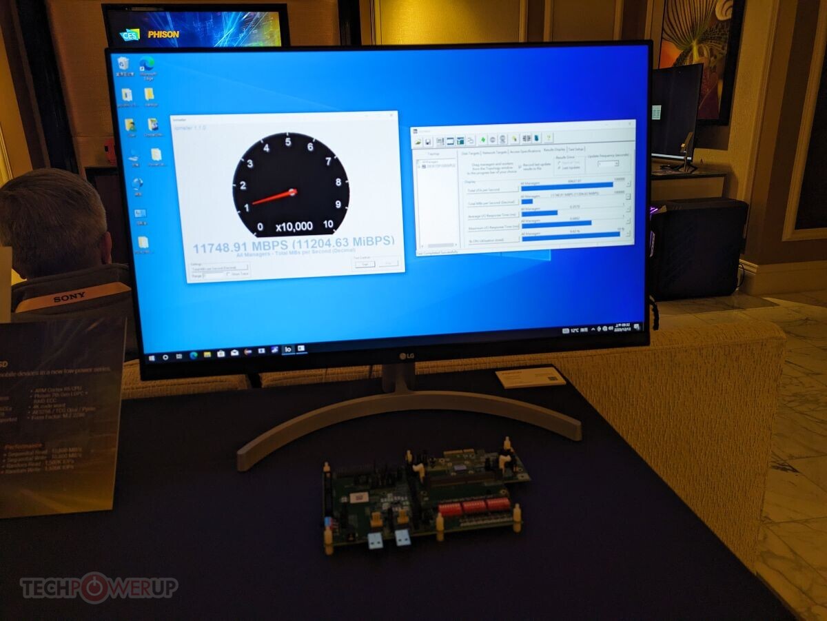
Sabrent today debuted the Rocket 4 line of DRAMless M.2 NVMe Gen 4 SSDs. Built in the M.2-2280 form-factor, these drives take advantage of the PCI-Express 4.0 x4 host interface, and provide sequential transfer speeds of up to 7.4 GB/s reads, with up to 6.4 GB/s writes. The drives also offer 4K random access performance of up to 1 million IOPS reads, and 0.95 million IOPS writes. For now, Sabrent is launching 1 TB and 2 TB capacity variants of the Rocket 4, but the company is preparing to launch a larger 4 TB variant soon.

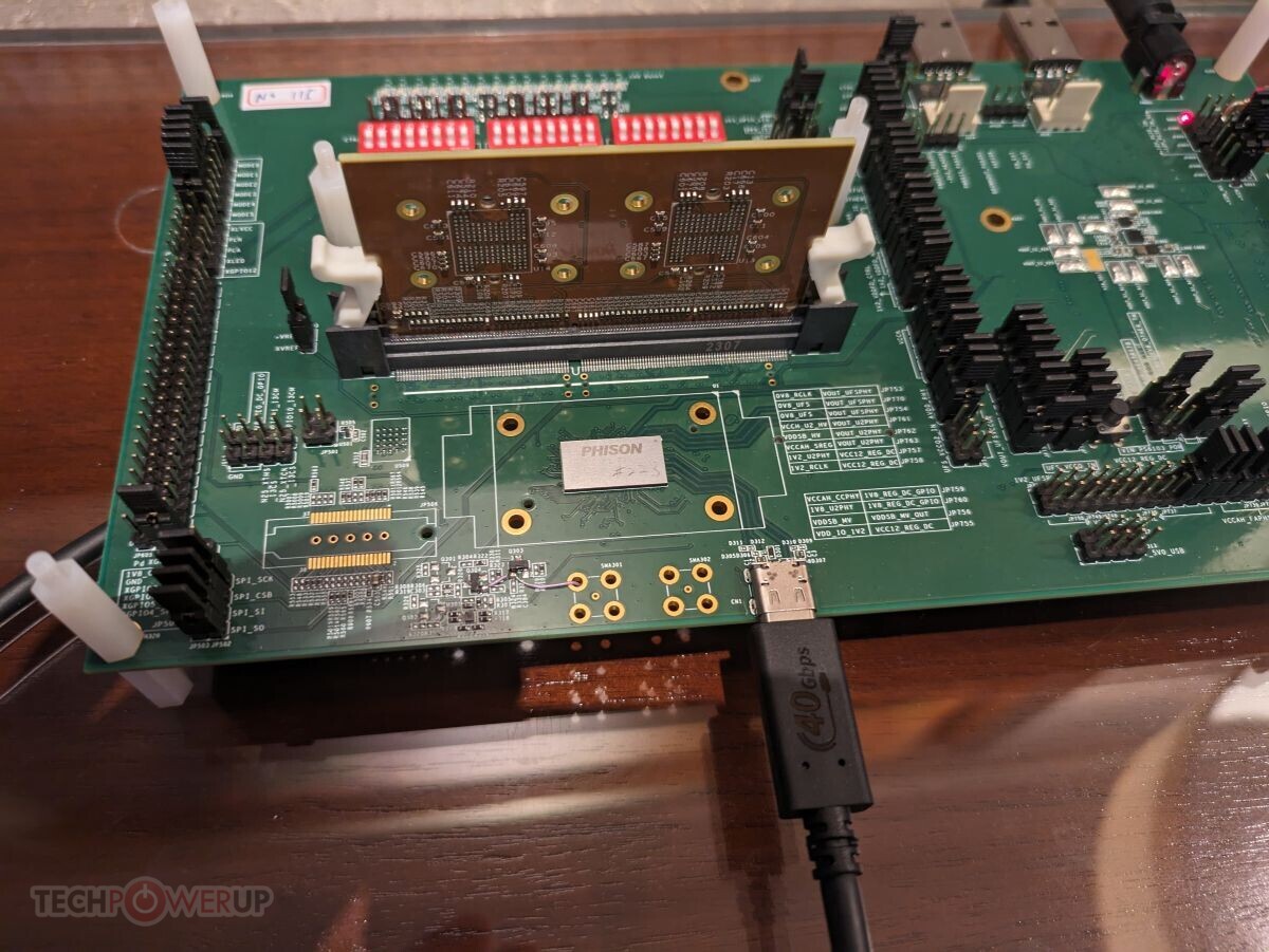
The Sabrent Rocket 4 combines a Phison E27T series DRAMless controller with Kioxia 162-layer 3D TLC NAND flash memory (also known as the BiCS 6). There's just a copper foil heat spreader to keep things cool. The 12 nm E27T doesn't run anywhere near as hot as the E18, so you can make do with the heatsink your motherboard includes, or run it the way it is. The 1 TB variant is priced at $99.99, and the 2 TB variant at $199.99. The company didn't reveal pricing of the unreleased 4 TB variant.

Loongson 3A6000 CPU Reportedly Matches AMD Zen 4 and Intel Raptor Lake IPC

China's homegrown Loongson 3A6000 CPU shows promise but still needs to catch up AMD and Intel's latest offerings in real-world performance. According to benchmarks by Chinese tech reviewer Geekerwan, the 3A6000 has instructions per clock (IPC) on par with AMD's Zen 4 architecture and Intel's Raptor Lake. Using the SPEC CPU 2017 processor benchmark, Geekerwan has clocked all the CPUs at 2.5 GHs to compare the raw benchmark results to Zen 4 and Intel's Raptor Lake (Raptor Cove) processors. As a result, the Loongson 3A6000 seemingly matches the latest designs by AMD and Intel in integer results, with integer IPC measured at 4.8, while Zen 4 and Raptor Cove have 5.0 and 4.9, respectively. The floating point performance is still lagging behind a lot, though. This demonstrates that Loongson's CPU design can catching up to global leaders, but still needs further development, especially for floating point arithmetic.

However, the 3A6000 is held back by low clock speeds and limited core counts. With a maximum boost speed of just 2.5 GHz across four CPU cores, the 3A6000 cannot compete with flagship chips like AMD's 16-core Ryzen 9 7950X running at 5.7 GHz. While the 3A6000's IPC is impressive, its raw computing power is a fraction of that of leading x86 CPUs. Loongson must improve manufacturing process technology to increase clock speeds, core counts, and cache size. The 3A6000's strengths highlight Loongson's ambitions: an in-house LoongArch ISA design fabricated on 12 nm achieves competitive IPC to state-of-the-art x86 chips built on more advanced TSMC 5 nm and Intel 7 nm nodes. This shows the potential behind Loongson's engineering. Reports suggest that next-generation Loongson 3A7000 CPUs will use SMIC 7 nm, allowing higher clocks and more cores to better harness the architecture's potential. So, we expect the next generation to set a bar for China's homegrown CPU performance.

Phison Launches Full Range of UFS Storage Solutions for Unparalleled Mobile Storage Performance

Phison Electronics, a leading provider of NAND controllers and NAND storage solutions, today announced it has introduced a full range of UFS (Universal Flash Storage) controllers (PS8325, PS8327, PS8329, PS8361). Phison's new UFS solutions support entry-level, middle, premium and flagship smartphone devices to achieve maximum performance in mobile storage and enhance user experiences.

As smartphone devices require higher performance, the storage devices of many entry-level 5G models have transitioned from eMMC to UFS 2.2 storage, and even flagship models of 4G phones have begun adopting the UFS 2.2 specification. Compared to the half-duplex mode of eMMC, the full-duplex mode of UFS 2.2 significantly increases read speeds by three times, not only handling smartphone functions that require processing large amounts of data (such as high-resolution recording and video playback), but also consuming lower power under the same performance speed as eMMC. This helps improve the battery life of smartphones and tablets, meeting the high-performance and low-power consumption needs of mobile devices.

Intel and UMC Announce New Foundry Collaboration

Intel Corp. and United Microelectronics Corporation ("UMC"), a leading global semiconductor foundry, today announced that they will collaborate on the development of a 12-nanometer semiconductor process platform to address high-growth markets such as mobile, communication infrastructure and networking. The long-term agreement brings together Intel's at-scale U.S. manufacturing capacity and UMC's extensive foundry experience on mature nodes to enable an expanded process portfolio. It also offers global customers greater choice in their sourcing decisions with access to a more geographically diversified and resilient supply chain.

"Taiwan has been a critical part of the Asian and global semiconductor and broader technology ecosystem for decades, and Intel is committed to collaborating with innovative companies in Taiwan, such as UMC, to help better serve global customers," said Stuart Pann, Intel senior vice president and general manager of Intel Foundry Services (IFS). "Intel's strategic collaboration with UMC further demonstrates our commitment to delivering technology and manufacturing innovation across the global semiconductor supply chain and is another important step toward our goal of becoming the world's second-largest foundry by 2030."

Team Group Releases T-Force GE PRO NVMe Gen 5 SSD

T-FORCE, the gaming brand of Team Group Inc., the world's leading memory and storage provider, today announced the release of the new generation of Gen 5 SSDs, the T-FORCE GE PRO PCIe 5.0 SSDs. This much-anticipated SSD is powered by InnoGrit's newest 12 nm, multi-core, and low-wattage IG5666 controller, equipped with a patented ultra-thin graphene heatsink and has read speeds of up to 14,000 MB/s. Supported by smart cooling and state-of-the-art error correction technologies, the T-FORCE GE PRO PCIe 5.0 SSD provides gamers with the next level of peak performance.

The T-FORCE GE PRO PCIe 5.0 SSD features InnoGrit's latest 12 nm, IG5666 controller, which has multiple cores and low power consumption. The SSD's read speed maxes out at 14,000 MB/s, and equipped with an enhanced controller feature called Security Isolation that utilizes isolation technology to protect data from external attacks, providing a reliable, multi-faceted defense. The GE PRO SSD also supports smart power management and thermal regulation technology, which detects different workload conditions through internal temperature sensing and automatically adjusts the power management mode to prevent overheating. The T-FORCE GE PRO PCIe 5.0 SSD enhances data transfer accuracy by correcting data errors with the brand new 4K LDPC (Low-Density Parity-Check Code) technology. It also supports Team Group's patented S.M.A.R.T. monitoring software, allowing gamers to monitor the health and performance of the SSD at any time.

Seagate's Breakthrough 30TB+ HDDs Ramp Volume

Seagate Technology, a world leader in sustainable mass-data storage solutions, today announced a milestone that marks a new era in the storage industry. The company launched the Mozaic 3+ hard drive platform—which incorporates Seagate's trailblazing implementation of Heat-Assisted Magnetic Recording (HAMR) technology. The launch heralds unparalleled areal densities of 3 TB+ per platter—and a roadmap that will achieve 4 TB+ and 5 TB+ per platter in the coming years.

The Mozaic 3+ platform powers Seagate's flagship Exos product family, with newly announced, industry-leading capacity points of 30 TB and beyond. Exos 30 TB+ products are shipping in volume this quarter to hyperscale cloud customers. Seagate's areal density innovation—which increases the number of bits that can be stored on a platter—addresses common industry pain points. Mozaic 3+ enables customers to store more data in the same floor space than ever before. Upgrading from a 16 TB conventional perpendicular magnetic recording (PMR) drive (the average capacity in large-scale data centers) to an Exos 30 TB Mozaic 3+ technology drive effectively doubles capacity in the same footprint.

Phison Embraces 7 Nanometer: Cooler PCIe Gen 5 SSDs Incoming With New Controller

The current crop of PCIe Gen 5 based M.2 NVMe SSDs run scorching hot to deliver sequential transfer speeds of 10 GB/s, requiring some massive cooling solutions with tiny fans. All this might change, as Phison, a leading SSD controller manufacturer, unveiled three new controllers at the 2024 International CES. One of these that stands out, is the PS5031-E31T, which is built on the 7 nm node, and could power the first Gen 5 SSDs delivering 10 GB/s without elaborate cooling solutions. This is a big upgrade from the 12 nm node used by their first Gen 5 controllers. The PS5031-E31T is a DRAMless controller meant for mainstream Gen 5 SSDs. This controller has a 4-channel flash interface (16 CE), a PCI-Express 5.0 x4 host interface, supports capacities of up to 8 TB, and is claimed by Phison to offer sequential transfer rates of up to 10.8 GB/s, and up to 1500K IOPS random access; exceeding the fastest Gen 4 SSDs.

Phison also updated its high-end controller lineup with the new PS5026-E26 Max14um. This is a variant of the E26 that's designed for the upcoming Micron B58R NAND flash chip that offers 2400 MT/s per channel transfers. Over the 8-channel interface of the E26, this finally unlocks sequential transfer speeds exceeding 14 GB/s reads, and 12.7 GB/s sequential writes. This is merely a revision of the existing E26 with updated power-optimized firmware, the underlying silicon is identical. The E26 Max14um is the first controller to surpass 1000 MB/s in all three PCMark 10 storage tests. We have a sample of an SSD powered by the E26 Max14um in our labs, and will post our review soon.

MSI Spatium M580 Liquid Frozr is an M.2 SSD with a Self Contained Liquid Cooling Loop

MSI Spatium M580 Liquid Frozr is easily one of the most interesting SSDs we've come across in CES 2024. Picture this—an M.2-2280 SSD that has a self-contained liquid cooler, complete with a fan, radiator, a pump-block, and coolant channels. This is both cute and a little sad. M.2 SSDs were supposed to stay out of sight and be completely cable-free, like DIMMs. This isn't MSI's fault, they have to use the fastest controllers in the market, which are built on older 12 nm foundry nodes. PCI-Express 5.0 x4 is comparable bandwidth to PCI-Express 3.0 x16, and moving this kind of data is bound to generate heat for an SSD controller. Enough banter—the Spatium M580 uses the fastest Phison E26 Max14um controller, with Micron's fastest B58R 232-layer 3D NAND flash chips that deliver 2400 MT/s per flash channel.

The combination of Phison Max14um and B58R results in sequential transfer speeds beyond the 14 GB/s mark, which is where most PCIe Gen 5 x4 drives will end up accounting for the interface+protocol overhead. The theoretical max bandwidth of Gen 5 x4 is 16 GB/s. The drive comes in capacities of up to 4 TB. As for the cooler's design, the bare drive makes contact with a copper cold-plate, which has the block+reservoir, with a tiny pump. This sends coolant through a real aluminium heat-exchanger—this is probably the smallest radiator we've ever seen. The radiator is held up, a supporting structure has a tiny 20 mm lateral-flow fan, which blows air through the radiator. We can't wait to review this thing!

Team Group Launches the T-FORCE GE PRO NVMe Gen 5 SSD

T-FORCE, the gaming brand under the leading memory and storage provider Team Group Inc., is committed to excellence in product research and development while constantly pushing the boundaries of limits. Today, Team Group is announcing the new Generation of Gen 5 SSD, the T-FORCE GE PRO PCIe 5.0 SSD which uses the PCIe Gen 5 x4 interface and NVMe 2.0 standard. The new multi-core, low-wattage Gen 5 SSD is designed for extreme storage speeds and is perfect for gamers and users who desire the ultimate performance.

The T-FORCE GE PRO PCIe 5.0 SSD is powered by InnoGrit's new 12 nm, multi-core, and energy-efficient IG5666 controller, paired with a high-performance 2,400MT/s NAND flash that supports DRAM and SLC caching with read speeds up to 14,000 MB/s. It features a smart thermal regulation technology that utilizes internal temperature sensors to automatically adjust performance and prevent overheating. It also supports 4K LDPC (low-density parity-check code) technology, which ensures data transfer accuracy. This allows the T-FORCE GE PRO SSD to provide excellent and stable performance, extending the product's lifespan. With Team Group's patented S.M.A.R.T. monitoring software, users can easily keep track of the SSD's health at any time.

Chinese Loongson 3A6000 CPU Matches Intel "Raptor Lake" IPC

The Chinese chipmaker Loongson has launched its newest desktop processors, the 4-core, 8-thread 3A6000 series, based on the company's LoongArch microarchitecture. We have previously reported that the company wants to match Intel's "Willow Cove" and AMD's Zen 3 instruction per clock (IPC) levels with its 3A6000 CPU series, and today we have the first preview of the performance. Powered by the LA664 cores, 3A6000 is built on a 14/12 nm manufacturing process, with clock speeds going from 2.0 to 2.5 GHz and power consumption of up to 50 Watts. It features 256 KB of L2 cache and 16 MB of L3 cache in total.

While several hardware partners are announcing new Loongson-powered solutions, ASUS China's "Uncle Tony" managed to get his hands on one of them and overclocker the CPU to 2.63 GHz on air cooling. In overclocking tests using liquid nitrogen cooling, a 3A6000 processor reached 3.0 GHz, though there are indications that there is still overhead. In standard out-of-the-box configuration, the 3A6000 performs similarly to Intel's Core i3-10100 four-core CPU, an achievement for Loongson but still behind Intel's latest offerings that clock nearly twice as high. This rapid development of Loongson IP has led to a massive performance increase, matching the IPC of modern CPUs. We are still left to see more information about these 3A6000 series SKUs; however, early benchmarks suggest a significant improvement. You can see the CPU benchmarks below, which include UnixBench and SPEC CPU 2006.

Samsung Electronics Unveils Industry's Highest-Capacity 12nm-Class 32Gb DDR5 DRAM

collaboration with diverse industries and support various applications
Samsung Electronics, a world leader in advanced memory technology, today announced that it has developed the industry's first and highest-capacity 32-gigabit (Gb) DDR5 DRAM using 12 nanometer (nm)-class process technology. This achievement comes after Samsung began mass production of its 12 nm-class 16Gb DDR5 DRAM in May 2023. It solidifies Samsung's leadership in next-generation DRAM technology and signals the next chapter of high-capacity memory.

"With our 12 nm-class 32Gb DRAM, we have secured a solution that will enable DRAM modules of up to 1-terabyte (TB), allowing us to be ideally positioned to serve the growing need for high-capacity DRAM in the era of AI (Artificial Intelligence) and big data," said SangJoon Hwang, Executive Vice President of DRAM Product & Technology at Samsung Electronics. "We will continue to develop DRAM solutions through differentiated process and design technologies to break the boundaries of memory technology."

Team Group and InnoGrit Partner to Develop 14 GB/s M.2 NVMe Gen 5 SSD

Team Group's gaming brand, T-FORCE's Z54A series, develops the pioneering new generation PCIe Gen 5 SSD with outstanding performance, with read and write speeds up to 14,000 MB/s and 10,000 MB/s, respectively. Team Group exclusively cooperates with globe-leading advancing storage supplier, InnoGrit Corporation, producing the ultra-fast PCIe SSD products for certain high-performance fields, such as computers, workstations, data centers, servers, gaming consoles, video making, and editing.

T-FORCE offers the most comprehensive heat-sink solutions for the M.2 SSD, tailored for the heat sinks of the ultra-fast Gen 5 PCIe SSD. The circular AIO liquid cooling systems with a Taiwanese invention patent (I778726) bring a group of high-level computer users the solution to the problem of low speed caused by the high-temperature operation of the PCIe M.2 SSDs. The solution that the T-FORCE M.2 SSD brings has the ability to perfectly release performance and extend the lifespan of SSDs. It is the product of the SSD heat sink that brings the benefit of saving power to the new generation.

Samsung Electronics Announces 12nm-Class 7.2 Gbps DDR5 DRAM Mass Production Start

Samsung Electronics, a world leader in advanced memory technology, today announced that its 16-gigabit (Gb) DDR5 DRAM, which utilizes the industry's most advanced 12 nanometer (nm)-class process technology, has started mass production. Samsung's completion of the state-of-the-art manufacturing process reaffirms its leadership in cutting-edge DRAM technology.

"Using differentiated process technology, Samsung's industry-leading 12 nm-class DDR5 DRAM delivers outstanding performance and power efficiency," said Jooyoung Lee, Executive Vice President of DRAM Product & Technology at Samsung Electronics. "Our latest DRAM reflects our continued commitment to leading the DRAM market, not only with high-performance and high-capacity products that meet computing market demand for large-scale processing but also by commercializing next-generation solutions that support greater productivity."

EdgeCortix Expands Delivery of its Industry Leading SAKURA-I AI Co-processor Devices

EdgeCortix Inc., the innovative Edge Artificial Intelligence (AI) Platform company, focused on delivering class-leading compute efficiency and ultra-low latency for AI inference; announced, it is shipping its industry leading, energy-efficient, turn-key, AI co-processor, branded as the EdgeCortix SAKURA-I, to its global Early Access Program members.

"We are very pleased to be announcing the fulfillment of our first-generation semiconductor solution, the EdgeCortix SAKURA-I AI co-processor. Designed and engineered in Japan, SAKURA-I features up to 40 trillion operations per second (TOPs) of dedicated AI performance at sub-10 watts of power consumption.", said Sakyasingha Dasgupta, CEO and Founder of EdgeCortix, "We are delivering a complete Edge AI platform to our Early Access Program members, comprising both software and hardware solutions, which includes our recently updated MERA software suite. Program members include numerous global industry leading enterprise customers across both the commercial and defense sectors. We developed the EdgeCortix Early Access Program (EAP) with a focus on offering customers the opportunity to assess EdgeCortix's products and services at scale, by deploying them within their own complex, heterogeneous environments. The goal of the EAP offering is three-fold: showcasing the ease of integration into customer's existing heterogeneous systems, enabling customers to prove-out the effectiveness and efficiency of EdgeCortix solutions versus competing products and facilitating a direct dialog with EdgeCortix product management, enabling tailor-made fit in certain cases."

Strict Restrictions Imposed by US CHIPS Act Will Lower Willingness of Multinational Suppliers to Invest

TrendForce reports that the US Department of Commerce recently released details regarding its CHIPS and Science Act, which stipulates that beneficiaries of the act will be restricted in their investment activities—for more advanced and mature processes—in China, North Korea, Iran, and Russia for the next ten years. The scope of restrictions in this updated legislation will be far more extensive than the previous export ban, further reducing the willingness of multinational semiconductor companies to invest in China for the next decade.

CHIPS Act will mainly impact TSMC; and as the decoupling of the supply chain continues, VIS and PSMC capture orders rerouted from Chinese foundries
In recent years, the US has banned semiconductor exports and passed the CHIPS Act, all to ensure supply chains decoupling from China. Initially, bans on exports were primarily focused on non-planar transistor architecture (16/14 nm and more advanced processes). However, Japan and the Netherlands have also announced that they intend to join the sanctions, which means key DUV immersion systems, used for producing both sub-16 nm and 40/28 nm mature processes, are likely to be included within the scope of the ban as well. These developments, in conjunction with the CHIPS Act, mean that the expansion of both Chinese foundries and multinational foundries in China will be suppressed to varying degrees—regardless of whether they are advanced or mature processes.

SK Hynix Enters Partner Verification Process of its 5th Gen 1β DRAM

Although DRAM is using much less refined production processes compared to the latest processors and GPUs, all the major manufacturers are continuing to shrink their manufacturing nodes step by step. Part of the reason for this, is that a node shrink doesn't have the same improvements for DRAM as it does for most types of field-effect transistors or FETs, which are mostly used for making processor logic of some kind. SK Hynix is now said to have entered the partner verification process of its 5th gen 1β DRAM, to make sure its latest 1x nm DRAM is compatible with major applications. In SK Hynix's case this should roughly translate to a 12 nm process node.

According to Chosun Media in Korea, Intel will take part in this verification, with Intel having finished verification of SK Hynix's 4th gen 1α DRAM for its 4th gen Xeon Scalable processor. Initially, SK Hynix's 5th gen 1β DRAM will be targeting server applications, so it's likely it will be tested for compatibility with the same platforms from Intel, among others. The new 1β DRAM is said to increase efficiency by more than 40 percent, although the publication didn't mention if this is power efficiency or something else. The 1β DRAM from SK Hynix, as well as Samsung—who announced its 1β DRAM in December 2022—are made using an EUV lithography process and the two Korean DRAM makers are the only two makers of DRAM that are using EUV so far.

Phison E26 Controller Powering Several Upcoming PCIe Gen 5 NVMe SSDs Detailed

At the 2023 International CES, we caught a hold of Phison, makes or arguably the most popular SSD controllers, which sprung to prominence on being the first to market with PCIe Gen 4 NVMe controllers, and now hopes to repeat it with PCIe Gen 5. We'd been shown a reference-design Phison E26-powered M.2 SSD, along with some hardware specs of the controller itself. The drive itself isn't much to look at—a standard looking M.2-2280 drive with a PCI-Express 5.0 x4 host interface, and the Phison E26 controller with its shiny IHS being prominently located next to a DDR4 memory chip, and two new-generation Micron Technology 3D NAND flash memory chips.

The Phison E26 controller, bearing the long-form model number PS5026-E26, is an NVMe 2.0 spec client-segment SSD controller. It has been built on the TSMC 12 nm FinFET silicon-fabrication node. The controller features an integrated DRAM controller with support for DDR4 and LPDDR4 memory types for use as DRAM cache. Its main flash interface is 8-channel with 32 NAND chip-enable (CE) lines, support for TLC and QLC NAND flash, a dual-CPU architecture, and hardware-acceleration for AES-256, TCG-Opal, and Pyrite. The controller features Phison's 5th generation LPDC ECC and internal RAID engines. For its reference-design 2 TB TLC-based drive, Phison claims sequential transfer rates of up to 13.5 GB/s reads, with up to 12 GB/s writes. The 4K random-access performance is rated at up to 1.5 million IOPS reads, with up to 2 million IOPS writes.

Samsung Electronics Develops Industry's First 12nm-Class DDR5 DRAM

Samsung Electronics Co., Ltd., the world leader in advanced memory technology, today announced the development of its 16-gigabit (Gb) DDR5 DRAM built using the industry's first 12-nanometer (nm)-class process technology, as well as the completion of product evaluation for compatibility with AMD. "Our 12 nm-range DRAM will be a key enabler in driving market-wide adoption of DDR5 DRAM," said Jooyoung Lee, Executive Vice President of DRAM Product & Technology at Samsung Electronics. "With exceptional performance and power efficiency, we expect our new DRAM to serve as the foundation for more sustainable operations in areas such as next-generation computing, data centers and AI-driven systems."

"Innovation often requires close collaboration with industry partners to push the bounds of technology," said Joe Macri, Senior VP, Corporate Fellow and Client, Compute and Graphics CTO at AMD. "We are thrilled to once again collaborate with Samsung, particularly on introducing DDR5 memory products that are optimized and validated on "Zen" platforms."

AMD Explains the Economics Behind Chiplets for GPUs

AMD, in its technical presentation for the new Radeon RX 7900 series "Navi 31" GPU, gave us an elaborate explanation on why it had to take the chiplets route for high-end GPUs, devices that are far more complex than CPUs. The company also enlightened us on what sets chiplet-based packages apart from classic multi-chip modules (MCMs). An MCM is a package that consists of multiple independent devices sharing a fiberglass substrate.

An example of an MCM would be a mobile Intel Core processor, in which the CPU die and the PCH die share a substrate. Here, the CPU and the PCH are independent pieces of silicon that can otherwise exist on their own packages (as they do on the desktop platform), but have been paired together on a single substrate to minimize PCB footprint, which is precious on a mobile platform. A chiplet-based device is one where a substrate is made up of multiple dies that cannot otherwise independently exist on their own packages without an impact on inter-die bandwidth or latency. They are essentially what should have been components on a monolithic die, but disintegrated into separate dies built on different semiconductor foundry nodes, with a purely cost-driven motive.

Lexar Announces Professional NM800PRO PCIe Gen4 SSD

Lexar, a leading global brand of flash memory solutions, is proud to announce the Lexar Professional NM800PRO M.2 2280 PCIe Gen4 x4 NVMe SSD, with a heatsink model also available. It is engineered for hardcore gamers, professionals and creators who demand high-performance computing.

The Lexar Professional NM800 M.2 2280 NVMe SSD provides maximum SSD performance that puts you in the computing fast lane with speeds up to 7500 MB/s read and 6500 MB/s write. With blazing-fast performance, the Lexar NM800 PRO SSD leverages the 12 nm controller to produce lower power consumption and longer battery life for all your high-performance computing needs. Unlike traditional hard disk drives, the Lexar NM800PRO SSD has no moving parts, so it's built to last. On top of that, it's also shock and vibration resistant, making it one robust and reliable SSD.
Update Sep 6th: Added pricing information.

AMD "Zen 4" Dies, Transistor-Counts, Cache Sizes and Latencies Detailed

As we await technical documents from AMD detailing its new "Zen 4" microarchitecture, particularly the all-important CPU core Front-End and Branch Prediction units that have contributed two-thirds of the 13% IPC gain over the previous-generation "Zen 3" core, the tech enthusiast community is already decoding images from the Ryzen 7000 series launch presentation. "Skyjuice" presented the first annotation of the "Zen 4" core, revealing its large branch-prediction unit, enlarged micro-op cache, TLB, load/store unit, and dual-pumped 256-bit FPU that enables AVX-512 support. A quarter of the core's die-area is also taken up by the 1 MB dedicated L2 cache.

Chiakokhua (aka Retired Engineer) posted a table detailing the various caches and their latencies, comparing it with those of the "Zen 3" core. As AMD's Mark Papermaster revealed in the Ryzen 7000 launch event, the company has enlarged the micro-op cache of the core from 4 K entries to 6.75 K entries. The L1I and L1D caches remain 32 KB in size, each; while the L2 cache has doubled in size. The enlargement of the L2 cache has slightly increased latency, from 12 cycles to 14. Latency of the shared L3 cache is also up, from 46 cycles to 50 cycles. The reorder buffer (ROB) in the dispatch stage has been enlarged from 256 entries to 320 entries. The L1 branch target buffer (BTB) has increased in size from 1 KB to 1.5 KB.

AMD Confirms Optical-Shrink of Zen 4 to the 4nm Node in its Latest Roadmap

AMD in its Ryzen 7000 series launch event shared its near-future CPU architecture roadmap, in which it confirmed that the "Zen 4" microarchitecture, currently on the 5 nm foundry node, will see an optical-shrink to the 4 nm process in the near future. This doesn't necessarily indicate a new-generation CCD (CPU complex die) on 4 nm, it could even be a monolithic mobile SoC on 4 nm, or perhaps even "Zen 4c" (high core-count, low clock-speed, for cloud-compute); but it doesn't rule out the possibility of a 4 nm CCD that the company can use across both its enterprise and client processors.

The last time AMD hyphenated two foundry nodes for a single generation of the "Zen" architecture, was with the original (first-generation) "Zen," which debuted on the 14 nm node, but was optically shrunk and refined on the 12 nm node, with the company designating the evolution as "Zen+." The Ryzen 7000-series desktop processors, as well as the upcoming EPYC "Genoa" server processors, will ship with 5 nm CCDs, with AMD ticking it off in its roadmap. Chronologically placed next to it are "Zen 4" with 3D Vertical Cache (3DV Cache), and the "Zen 4c." The company is planning "Zen 4" with 3DV Cache both for its server- and desktop segments. Further down the roadmap, as we approach 2024, we see the company debut the future "Zen 5" architecture on the same 4 nm node, evolving into 3 nm on certain variants.

ASUS ROG Strix SQ7 Specifications Finally Revealed

Just under a month ago, ASUS posted a teaser for its first internal SSD, the ROG Strix SQ7 and now the company has finally released the full specs. It is indeed based around the 12 nm Phison E18 controller, as predicted by our Editor-In-Chief, something he spotted from the sneak peek picture. Although ASUS didn't specifically mention what kind of flash the drive is using, they kindly left the flash model number visible in one of its pictures of the drive. Although the full model name isn't visible, enough of it is visible to identify it as Micron's 176-layer TLC flash. The ROG Strix SQ7 also sports a DDR4 cache, as expected, although ASUS doesn't mention clock speeds.

ASUS claims the drive will deliver sequential read speeds of up to 7000 MB/s and write speeds of up to 6000 MB/s, which places the ROG Strix SQ7 in direct competition with several other Phison E18 based high-end drives from the likes of Kingston, MSI, Sabrent and others. Unfortunately, ASUS doesn't mention IOPS or random performance, although an unspecified "large" SLC cache is mentioned. Other features include TGC Opal and AES 256-bit encryption. ASUS also provides its own SSD dashboard, which of course is ROG branded, but looks like a skinned version of Phison's standard SSD dashboard, rather than something custom made. ASUS also provides a copy of NTI Backup Now EZ software and the drives appear to have a five year warranty. ASUS mentions PS5 compatibility outside of the PC space. No word on pricing or retail availability was provided and so far ASUS has only listed a 1 TB model.

AMD EPYC "Genoa" Zen 4 Processor Multi-Chip Module Pictured

Here is the first picture of a next-generation AMD EPYC "Genoa" processor with its integrated heatspreader (IHS) removed. This is also possibly the first picture of a "Zen 4" CPU Complex Die (CCD). The picture reveals as many as twelve CCDs, and a large sIOD silicon. The "Zen 4" CCDs, built on the TSMC N5 (5 nm EUV) process, look visibly similar in size to the "Zen 3" CCDs built on the N7 (7 nm) process, which means the CCD's transistor count could be significantly higher, given the transistor-density gained from the 5 nm node. Besides more number-crunching machinery on the CPU core, we're hearing that AMD will increase cache sizes, particularly the dedicated L2 cache size, which is expected to be 1 MB per core, doubling from the previous generations of the "Zen" microarchitecture.

Each "Zen 4" CCD is reported to be about 8 mm² smaller in die-area than the "Zen 3" CCD, or about 10% smaller. What's interesting, though, is that the sIOD (server I/O die) is smaller in size, too, estimated to measure 397 mm², compared to the 416 mm² of the "Rome" and "Milan" sIOD. This is good reason to believe that AMD has switched over to a newer foundry process, such as the TSMC N7 (7 nm), to build the sIOD. The current-gen sIOD is built on Global Foundries 12LPP (12 nm). Supporting this theory is the fact that the "Genoa" sIOD has a 50% wider memory I/O (12-channel DDR5), 50% more IFOP ports (Infinity Fabric over package) to interconnect with the CCDs, and the mere fact that PCI-Express 5.0 and DDR5 switching fabric and SerDes (serializer/deserializers), may have higher TDP; which together compel AMD to use a smaller node such as 7 nm, for the sIOD. AMD is expected to debut the EPYC "Genoa" enterprise processors in the second half of 2022.

Moore Threads Unveils MTT S60 & MTT S2000 Graphics Cards with DirectX Support

Chinese company Moore Threads has unveiled their MTT GPU series just 18 months after the company's establishment in 2020. The MT Unified System Architecture (MUSA) architecture is the first for any Chinese company to be developed fully domestically and includes support for DirectX, OpenCL, OpenGL, Vulkan, and CUDA. The company announced the MTT S60 and MTT S2000 single slot desktop graphics cards for gaming and server applications at a recent event. The MTT S60 is manufactured on a 12 nm node and features 2,048 MUSA cores paired with 8 GB of LPGDDR4X memory offering 6 TFLOPs of performance. The MTT S2000 is also manufactured on a 12 nm node and doubles the number of MUSA cores to 4096 paired with 32 GB of undisclosed video memory allowing it to reach 12 TFLOPs.

Moore Threads joins Intel in supporting AV1 encoding on a consumer GPU with MUSA cards featuring H.264, H.265, and AV1 encoding support in addition to H.264, H.265, AV1, VP8, and VP9 decoding. The company is also developing a physics engine dubbed Alphacore which is said to work with existing tools such as Unity, Unreal Engine, and Houdini to accelerate physics performance by 5 to 10 times. The only gaming performance shown was a simple demonstration of the MTT S60 running League of Legends at 1080p without any frame rate details.
Return to Keyword Browsing
May 1st, 2024 06:45 EDT change timezone

New Forum Posts

Popular Reviews

Controversial News Posts