News Posts matching #40 nm

Return to Keyword Browsing

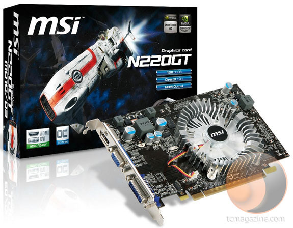
AMD Outs Radeon HD 6670, HD 6570, HD 6450 for OEMs

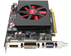
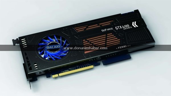
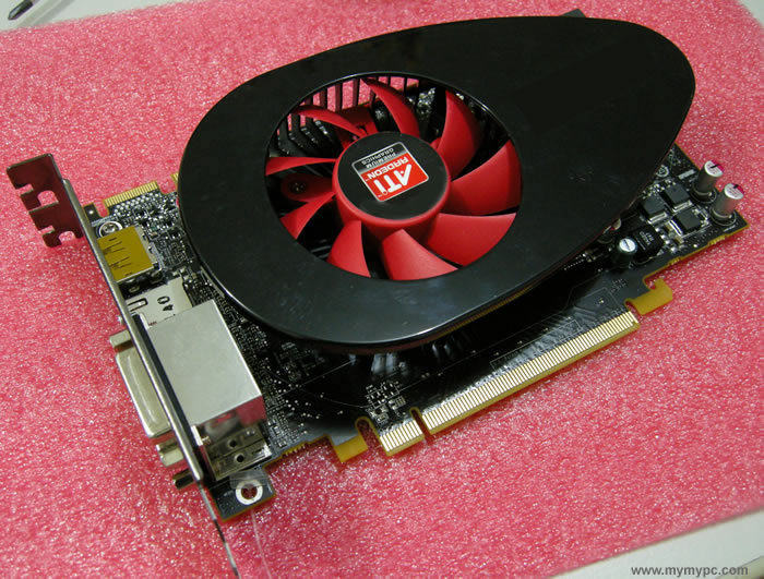
AMD released the entire entry-mid portion of the Radeon HD 6000 series overnight, for OEMs only. The cards won't be available to consumers (retail) as yet, but does give away specifications of two new GPUs that AMD is carving these SKUs out of, Turks and Caicos. Built on the 40 nm process, Turks packs 480 VLIW5 stream processors, is DirectX 11 compliant, and sports a 128-bit wide GDDR5 memory controller that supports GDDR3 on lower SKUs. Radeon HD 6670 and HD 6570 are based on Turks. Both have all 480 stream processors enabled, differ in memory type/amount and clock speeds. The HD 6670 carries clock speeds of 800 MHz core, 1000 MHz (4.00 GHz GDDR5 effective) memory, and is available with memory amounts of 512 MB or 1 GB. The 128-bit wide memory interface churns out bandwidth of 64 GB/s.

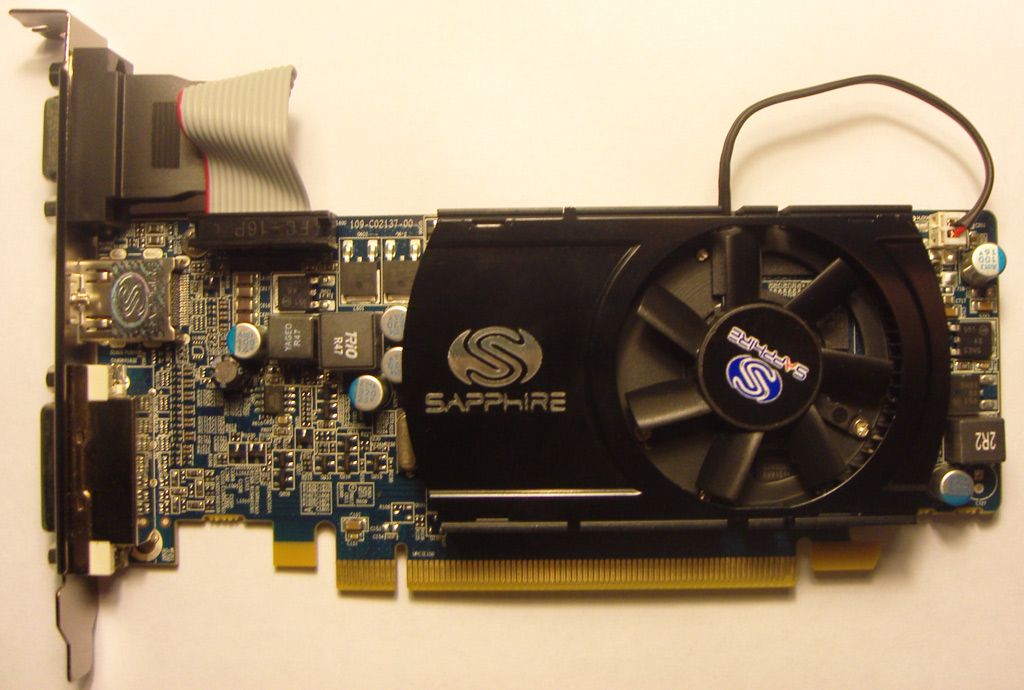
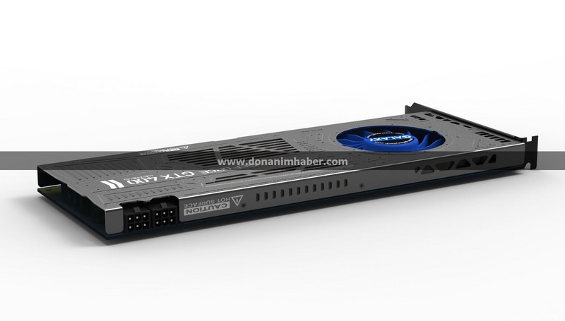
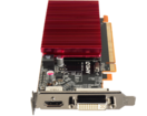
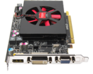
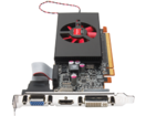
The HD 6570 is also based on Turks, but features clock speeds of 650 MHz core, and two different memory clock speed specifications based on the memory type opted for by the manufacturers. If a manufacturer chooses GDDR3, it's clocked at 900 MHz (1.80 GHz GDDR3 effective), with a memory bandwidth of 28.8 GB/s. If it's GDDR5, it's clocked at 1000 MHz (4.00 GHz effective), 64 GB/s bandwidth. Up to 2 GB of memory can be opted for GDDR3 designs, while up to 1 GB can be opted for GDDR5-based ones. While the HD 6670 reference board uses a full-height design with a single-slot fan-heatsink, HD 6570 is designed for low-profile cards, best suited for HTPCs or SFF PCs.

EVGA Intros GeForce GTX 570 HD Graphics Card

EVGA rolled out a new custom-design GeForce GTX 570 graphics card that makes use of a shorter PCB and a cooler design inspired from that of the GeForce GTX 560 Ti, which offers better high-definition display connectivity compared to the standard model. Called the EVGA GeForce GTX 570 HD (model: 012-P3-1571-AR), the card makes use of a shorter GTX 570 PCB the company earlier displayed at CES with a yet unreleased dual-fan GTX 570. Display connectivity on this card includes two DVI, a full-sized (standard) HDMI 1.4, and a full-sized DisplayPort.

The cooler design is largely borrowed from NVIDIA's reference GeForce GTX 560 Ti, consisting of a circular heatsink with spirally-projecting aluminum fins, spreading heat to additional aluminum fin blocks on its either sides. It is ventilated by a large centrally-located fan. The card sticks to NVIDIA reference clock speeds of 732 MHz core, 1464 MHz CUDA cores, and 950 MHz (3800 GDDR5 effective) memory. Based on the 40 nm GF110 core, the GPU packs 480 CUDA cores, and connects to 1280 MB of memory over a 320-bit wide GDDR5 memory interface. EVGA's GeForce GTX 570 HD is priced at $349.99, on par with the reference base model.

Toshiba and GlobalFoundies in Talks for Chip Manufacture Deal

Prospects are looking brighter by the day for GlobalFoundries, as the firm is reportedly in talks with Toshiba to strike a chip foundry partner deal. The deal will give GlobalFoundries contract to manufacture any or many of the plethora of chips Toshiba uses in computer hardware and consumer electronics. On GlobalFoundries' side, Doug Grose, chief executive officer of the American foundry, told Nikkei that the two firms are in the final stages of negotiations.

"We had been considering outsourcing production to Samsung Electronics Co and GlobalFoundries since last year," said a Toshiba official. With this deal, Toshiba is looking for 28 nm and 40 nm class manufacturing, thereby cutting a chunk of its R&D, and making its engineers focus on chip design. Parallel to this, a deal with Samsung will allow the Korean electronics giant to manufacture low-cost image-processing chips, while GlobalFoundries manufactures products with the latest-technologies.

Palit Readies 3 GB GeForce GTX 580 Graphics Card, Too

What happens in Gainward, stays in Palit. Gainward's parent company, Palit, is also readying a GeForce GTX 580 graphics card with 3 GB memory, like its subsidiary. Featuring a non-reference PCB and cooling assembly, Palit's latest card uses twelve 2 Gbit GDDR5 memory chips over a 384-bit wide memory interface to achieve 3072 MB (3 GB) in total. It features a more traditional-looking cooler compared to the Gainward GTX 580 Phantom; which makes use of two fans to cool a large aluminum fin array. Palit's card is clocked at 783 MHz (core), 1566 MHz (CUDA cores), and 1005/4020 MHz (memory actual/effective). Based on the 40 nm GF110 core, the GTX 580 features 512 CUDA cores, and is compliant with the latest in consumer graphics technologies.

Gigabyte Intros New Cheap DDR3-Based HD 5670 Graphics Card

Gigabyte introduced a new Radeon HD 5670 based graphics card that is intended to be cost-effective. Carrying the model number GV-R567D3-1GI, it makes use of 1 GB of DDR3 memory instead of GDDR5. The 1 GB of memory is clocked at 800 MHz (1600 MHz DDR), installed across a 128-bit wide memory interface. The standard HD 5670 features 1 GB of GDDR5 memory clocked at 1000 MHz (4000 MHz GDDR5 effective). The HD 5670 GPU is clocked at 775 MHz. Based on the 40 nm Redwood core, it features 400 stream processors. Other features specific to Gigabyte's design include a silent double-slot cooler that makes use of an 80 mm fan, and display connectivity that includes one each of DVI, D-Sub, and a gold-plated HDMI port. Gigabyte did not give out a price, though one can expect it to be a little lower than that of the standard HD 5670.

Gigabyte Rolls Out Overclocked GeForce GTX 570 Graphics Card

Gigabyte graced NVIDIA's GeForce GTX 570 launch with a reference design graphics card model. Carrying the model number GV-N580D5-15I-B, Gigabyte's card features factory-overclocked speeds of 772 MHz (core), 1544 MHz (CUDA cores), and 1002/4008 MHz (memory/GDDR5 effective), against reference clock speeds of 732/1464/3800 MHz. Based on the 40 nm GF110 GPU, the GeForce GTX 570 features 480 CUDA cores, and connects to 1280 MB of memory over a 320-bit GDDR5 memory interface Gigabyte's GV-N580D5-15I-B is priced at US $359.99.

PowerColor Readies Radeon HD 6870 PCS+ Graphics Card

Back at its launch, AMD didn't allow its board partners to release custom-design Radeon HD 6870 graphics cards right away, though such a restriction wasn't in place for the HD 6850. They were, however, allowed to come up with factory-overclocked models, that stick to the AMD reference design. That restriction could soon be lifted, with one of the first pictures of a completely non-reference design HD 6870 graphics card, the PowerColor HD 6870 PCS+, smiling for cameras.

The Professional Cooling System Plus (PCS+) from PowerColor makes use of a high-grade cooler that facilitates better overclocking, and runs quieter compared to the reference design cooler. It consists of a racy-looking shroud under which there's a large GPU heatsink, which is cooled by a 90 mm fan. The PCB also looks to be non-reference design. The card is also overclocked out of the box, 940/4400 MHz (core/memory, GDDR5 effective), vs. reference speeds of 900/4200 MHz. The Radeon HD 6870 is based on the 40 nm "Barts" silicon, it packs 1120 stream processors, and connects to 1 GB of memory over a 256-bit wide GDDR5 memory interface. The PowerColor HD 6870 PCS+ is expected to release towards the end of this month.

Sapphire HD 5550 Rebranded to HD 6390 for Russian Market

After the Radeon HD 6800 series, the rest of AMD's Northern Islands family of GPUs seem to be taking their own sweet time making it to the market. With the HD 6900 series almost certain to be off its November 22 launch date, lower-end GPUs slated for early 2011 are still far away. Meanwhile Sapphire reportedly took the opportunity to rebrand the existing "Redwood" based Radeon HD 5550 to "Radeon HD 6390", in a bid to make some monies in Russia.

The Radeon HD 6300, at least the HD 6350, HD 6370 are reserved for an upcoming GPU codenamed "Caicos", its AMD reference board even made it through a casual photo-session. The HD 5550 and HD 6390 were found to have the same device IDs. An older version of GPU Caps Viewer detects it as HD 5550, while the latest version sees it as HD 6390. The HD 5550 is based on the 40 nm "Redwood" GPU, it has 320 out of 400 stream processors enabled, and a 128-bit wide memory interface to typically connect to GDDR3 memory. Some premium models also feature GDDR5 memory.

Galaxy Designs Single-Slot GeForce GTX 460 Graphics Card

Galaxy is working on a new GeForce GTX 460 graphics card that uses a single-slot cooling solution. The company earlier surprised many, when it unveiled a single-slot GeForce GTX 470. Galaxy's new single-slot GTX 460 bears a long PCB, and a cooling solution that looks to make lavish use of copper. It also doesn't compromise on the clock speeds in any way, with the GPU running at 675 MHz, and memory at 900/3600 MHz effective. There is 1 GB of GDDR5 memory. The 40 nm GF104 core is DirectX 11 compliant, and has 336 CUDA cores enabled on this card. The card draws power from two 6-pin power inputs. It is SLI capable. Galaxy didn't give out details about pricing and availability, importantly if it will be available to the western markets in the first place.

AMD Radeon HD 6850 Specs, Pricing Surfaces

AMD's latest graphics processors is just around the corner, and one of the first of them is the Radeon HD 6800 series. The value version of it is the Radeon HD 6850, its most probable specifications have surfaced. To begin with, HD 6850 is based on AMD's new Barts GPU, built on the 40 nm process. The source mentions that the SKU will have 800 stream cores enabled, from earlier reports we're lead to believe that these stream cores are individually more complex than AMD's traditional 5D (4 simple + 1 complex) approach to unified shaders. There is a 256-bit wide GDDR5 memory interface holding 1 GB of memory, the card uses 5 GT/s memory chips, so the memory should be clocked around 1200 MHz (or 4800 MHz effective), if not more. The core is clocked at 775 MHz. Its FOB (freight on board) price is expected to be US $175. Power is drawn from a single 6-pin PCI-E power connector, the draw is expected to be less than 150W. Partners have the option of using a premium blower-type cooler, or a cost-effective heatsink-type cooler. The latter had been pictured a while back, posted below for reference.

Point of View Intros its Low-Profile GeForce GT 430 Graphics Card

Point of View kicked of its GeForce GT 430 lineup with a custom-design graphics card. The card sticks to NVIDIA's reference design as far as the PCB goes, but uses a [seemingly] more cost-effective GPU cooling solution. The card is low-profile, and makes extra-room for a D-Sub connector with its full-height bracket on. Other connectors include DVI and HDMI. Like every other GeForce GT 430, Point of View's card is based on the 40 nm GF108 GPU, it is DirectX 11 compliant, and has 96 CUDA cores, a 128-bit wide DDR3 memory interface holding 1 GB of memory, and clock speeds that stick to NVIDIA's reference speeds: 700/1400/1600 MHz (core/shader/memory). A slightly faster variant based on the same exact design is also available, it just has the memory clocked 200 MHz higher. Expect standard pricing for this card.

Listing Reveals Details of GeForce GT 430 Desktop GPU

An Austrian hardware vendor jumped the gun and listed an unannounced GeForce GT 430 graphics card by Gigabyte, the GV-N430OC-1GI. As the model name suggests, it is overclocked out of the box. Tiny bits of details given in the listing shows that the card has 1 GB of DDR3 memory across a 128-bit wide memory interface, and connectors that include one each of DVI and HDMI. Additional detailed mentioned by a price aggregator reveals that GeForce GT 430 is based on the 40 nm GF108 core, the SKU has 96 CUDA cores and 16 TMUs.

Bulldozer-based Orochi and Fusion Llano Die Shots Surface in GlobalFoundaries Event

The first official die-shots of the first Bulldozer architecture derivative, the eight-core "Orochi" Opteron die was displayed at Global Technology Conference, by GlobalFoundries, AMD's principal foundry-partner. While AMD did not give out a die-map to go with it, the structures we can make out are four Bulldozer modules holding two cores and a shared L2 cache each, a L3 cache spread across four blocks that's shared between all cores, the northbridge-portion cutting across the die at the center, and the integrated memory controller along its far-right side. Various I/O portions are located along the other three sides.

Next up is the Llano die. This is AMD's very first Fusion APU (accelerated processing unit) die. It is based on the K10 architecture and integrates a graphics processor and northbridge completely into one die. It precedes APUs based on the Bobcat architecture. Fortunately, there is a die-map at hand, which shows four K10 cores with dedicated 1 MB L2 caches per core, no L3 cache, an integrated SIMD array that holds 480 stream processors. The GPU component is DirectX 11 compliant. Other components include an integrated northbridge, integrated memory controller, integrated PCI-Express root complex, and HyperTransport interface to the chipset.

Gigabyte Intros HD 5770 Silent Cell Graphics Card

Gigabyte is readying a new passively-cooled Radeon HD 5770 graphics card called the Gigabyte HD 5770 Silent Cell, carrying model number GV-R577SL-1GD. This 100% non-reference design card is built using Gigabyte's Ultra Durable VGA technology (comprising of 2 oz copper PCB, ferrite-core chokes, Low RDS (on) MOSFETs, and binned high-performance memory chips. What's more peculiar is its large GPU cooler that covers the length and height of the card, and extends a couple of inches over the length of the card. At its end, the heatsink also extends a good couple of inches over the height of the card, some of its fins even protrude out of the rear panel. The heatsink is a densely-packed aluminum fin array to which heat is conveyed by four 6 mm thick heat pipes.

Cooling assembly aside, the card sticks to AMD reference clock speeds - 850 MHz core, 1200 MHz (4800 MHz effective) memory, and uses 1 GB of GDDR5 memory across a 128-bit wide memory interface. The 40 nm Juniper GPU packs 800 stream processors, and supports the latest PC graphics technologies including DirectX 11. The card can pair with up to three more of its kind for CrossFireX. Display connectivity options include one each of DVI, HDMI, and DisplayPort. Gigabyte did not give out a price.

ATI Radeon HD 6000 Series ''Southern Islands'' Graphics Cards For Sale from November

Come this Winter, and things will heat up once again in the graphics card industry, with GPU vendors battling it out for the crucial Holidays shopping season. While AMD did not introduce any new GPUs after completing its ATI Radeon HD 5000 series launch itinerary, it did manage to grab significant amount of sales from its graphics rival NVIDIA. For this Winter, AMD and its partners will be in a position to launch the ATI Radeon HD 6000 series graphics processors, according to DigiTimes, citing sources from graphics card vendors.

It is also said that the Radeon HD 6000 series, codenamed "Southern Islands" (members of which are codenamed after islands in the Mediterranean Sea), will be built on TSMC's 40 nm manufacturing process. AMD had originally planned to build Southern Islands on TSMC's 32 nm process, but with the foundry skipping 32 nm bulk for 28 nm which will start operations only by the end of the year, AMD redrew its plans and stuck to the now-mature (stable) 40 nm process. Perhaps AMD learned a thing or two from a wide range of teething problems that plagued the 40 nm production line.

GeForce GTX 460 to Come in Distinct Variants, Launch Date Surfaces

The much talked about upcoming GeForce GTX 460 GPU from NVIDIA was recently pictured and detailed. Out of its first, grainy pictures, it became clear that the GF104 core it's based on indeed supports a 256-bit wide GDDR5 memory interface, but that only six of its eight 32-bit wide channels were occupied (192-bit), yielding 768 MB of memory. Fresh reports suggest that NVIDIA indeed will release the GeForce GTX 460 in two variants, a 768 MB one, and a 1024 MB (1 GB). The 1 GB variant by design will be faster, even if an application doesn't need all its video memory, because it will have a wider 256-bit memory interface, that's 25% higher memory bandwidth. Both variants will have the same memory clock speed of 900 MHz (3600 MHz effective). The GF104 core will be clocked at 675 MHz on both models, with 336 CUDA cores. Built on the 40 nm process at TSMC, the GeForce GTX 460 768 MB will have a TDP of 150W, while the 1 GB model will have a TDP of 160W. New reports suggest that the 768 MB model will be priced at less than $200. NVIDIA will release the GeForce GTX 460 on the 12th of July.

NVIDIA Readying GeForce 400 Series Mobile GPUs for June?

Call it a slip of the keyboard, the latest online build to order catalogue of Eurocom's performance laptops includes a new choice of graphics board, the "NVIDIA GeForce GTX 480M". It's not as much the entry, but details next to it that are interesting. This card, according to Eurocom, is said to be based on the Fermi architecture, is compliant with DirectX 11 (so it's not yet another re-branding), is built on the 40 nm manufacturing process, and has a power rating of [just] 100W. The card is compliant with the MXM 3.0b board standard. Eurocom sets the option's ETA to June 2010, and adds 271€ over the base configuration. In comparison, the GeForce GTX 285M SLI option (based on two G92 GPUs) asks for 339€ over the base configuration.

While by notebooks' standards 100W is on the higher side, it is astoundingly low by standards of NVIDIA's GeForce Fermi architecture, serving as a reasonable indication of NVIDIA's more energy-efficient Fermi-derived GPUs arriving to the scene in June. At the moment, unreliable sources point at NVIDIA expanding its GeForce 400 series lineup further down performance and mainstream segments, coinciding with Computex 2010 held in Taiwan.

TSMC Claims 40 nm Yield Issues Resolved

TSMC, one of the world's major semiconductor foundries, said that it has resolved all issues pertaining to proper yields of chips built on the 40 nanometre node. During a company event on the 19th, Mark Liu, Senior VP of Operations, said that the quality of production on the 40 nm node is almost on par with the 65 nm one. Liu stated that the chamber matching problems that had impacted yield rates for the company's 40nm node have been resolved.

TSMC caters to graphics processor giants NVIDIA and AMD, with both having designs of 40 nm performance graphics processors with multi-billion transistor counts. AMD has been selling 40 nm GPUs made by TSMC since its previous generation ATI Radeon HD 4770, it currently makes all its Radeon HD 5000 series GPUs on the node. NVIDIA is poised to release its first billion transistor 40 nm GPU, the GF100, in its consumer GeForce brand later this quarter.

In addition to this, TSMC has just finished building a new factory at the Hsinchu Science Park (HSP), Taiwan, part of its Fab 12. The new facility will be able to commence volume production of 28 nm products as early as by Q3 2010.

Hynix Introduces World's First 40 nm Class 2 Gb GDDR5 DRAM

Hynix Semiconductor Inc., today announced the industry's first 2 Gb (Gigabit) GDDR5 called H5GQ2H24MFR-R2C using its leading-edge 40nm class process technology.

The newly developed GDDR5 is the fastest and highest density graphics memory available in the market. It operates at 7 Gbps (Gigabit per second) bandwidth and processes up to 28 GB/s (Gigabytes per second) with a 32-bit I/O. In addition to its fastest speed and highest density, it is also designed to minimize power consumption with 1.35V operation voltage. It is an 'eco-friendly' device which reduces energy consumption by 20% over the preceding memory solutions using 50nm class technology.

ASUS Ready with EAH5770 CuCore Graphics Card

With the recent spurt of non-reference design Radeon HD 5770 graphics cards, ASUS seems to be ready with its EAH5770 CuCore, where "CuCore" stands for copper (Cu) core, used in the GPU cooler. Speaking of which, the GPU cooler consists of a GPU base which has 5.8 oz (164.5 g) of copper, for better transfer of heat, to the rest of the heatsink which has radially-projecting aluminum fins. The PCB designed by ASUS seems to be slightly longer than the reference AMD PCB, yet it only makes room for one CrossFire connector, meaning its can pair with only one more card of its kind (or up to three more cards with two CrossFire connectors).

The 40 nm Juniper GPU has DirectX 11 compliance, and is powered by 800 stream processors, and connects to 1 GB of memory across a 128-bit GDDR5 memory interface. Despite the swanky cooling the card sticks to reference AMD clock speeds of 850/1200 MHz (core/memory), but comes with the ASUS VoltageTweak feature that allows software voltage adjustments. The rear-panel is redesigned too, with one of the slots making for a large vent, with the lower slot holding one each of DVI-D, D-Sub, and HDMI. The ASUS EAH5770 CuCore is expected to be priced under 130 EUR.

Sapphire Unveils HD 5770 Vapor-X

Sapphire expanded its Radeon HD 5700 series with the Sapphire HD 5770 Vapor-X. This release comes around a month after the HD 5750 Vapor-X, and resembles it in having the same GPU cooler: a GPU contact block with a Vapor chamber acts as a large heatpipe, uniformly conveying heat to the heatsink above it, which is cooled by a fan. Unlike the HD 5750 Vapor-X which comes with a blue reference PCB, this one retains the black reference one, with the cooler being the only noticeable change.

The Radeon HD 5770 is based on the 40 nm Juniper GPU. It is DirectX 11 compliant, and has 800 stream processors, along with 1 GB of memory installed across a 128-bit GDDR5 interface. It also supports the ATI Eyefinity technology that allows users to scale a display head across three physical displays. Connectivity includes two DVI-D, and one each of HDMI and DisplayPort. Sapphire also gave it a modest factory overclock, with the core running at 860 MHz (vs 850 MHz reference), while the memory stays at 1200 MHz (4.8 GHz effective). It is priced around 145 EUR.

XFX Announces its Radeon HD 5970 Graphics Card

XFX takes technology for a trip down the fast lane with the debut of The XFX ATI Radeon HD 5970 graphics card. The fastest dual GPU-on-a-PCB card on the planet, in addition to the base powerhouse, this card also comes in an "I've-never-seen-that-kind-of-performance-before" Black Edition with an exclusive performance enhancing Overvolt Tool.

Created for the true performance enthusiast, this card offers the ultimate in speed, with the XFX ATI Radeon HD 5970 scoring in excess of X10000 in 3DMarkVantage v. 101, the highest single graphics card score achieved to date. It also features all of the latest, state-of-the-art technologies that hardcore gamers want, including ATI Eyefinity technology, ATI Stream technology and full DirectX 11 support.

AMD Introduces ATI Radeon HD 5700 Series Graphics Processors

AMD today released its ATI Radeon HD 5700 series of mid-range graphics processors aimed to increase the company's competitiveness in the sub-$200 market, and present a mainstream graphics card series compliant with the DirectX 11 API. The series makes use of AMD's 40 nm Juniper graphics processor, that packs 1.04 billion transistors, 800 stream processors, 40 texture units, and 16 raster operation units. The 128-bit wide GDDR5 memory interface provides up to 76.8 GB/s of memory bandwidth.

The higher-end product of the two on offer, Radeon HD 5770 is priced around the $150 mark, and has all its 800 stream processors and 40 texture units enabled. It comes with clock speeds of 850/1200 MHz (core/memory), while the Radeon HD 5750 looks to cash in on the $120 point. It has 720 stream processors, 36 texture units enabled from its kitty, with clock speeds of 700/1150 MHz (core/shader). While the Radeon HD 5770 comes with 1 GB of memory, the Radeon HD 5750 comes in variants of 1 GB and 512 MB. Some of the other big selling points of these cards are low rater power consumptions of 16~18 W at idle, and 86~108 W at load. The connectivity options include two DVI-D, and one each of DisplayPort and HDMI. The cards support AMD's Eyefinity technology which allows combining three 2560x1600 pixel display-heads for a single large display head. Each of these can pair with up to three more of its kind for 4-way CrossFireX multi-GPU performance upscaling.

All major AMD board vendors, such as ASUS, Sapphire, HIS, PowerColor, Gigabyte, MSI, VisionTek, XFX, among others, have their offerings based on these GPUs ready to sell from today. Pictured below (in order) are Radeon HD 5770 and Radeon HD 5750.

MSI GeForce GT 220 1 GB OC Pictured

NVIDIA has the launch of its GeForce GT 220 graphics processor lined up for next week. Aimed to be a sub-$100 lower-mainstream offering, the GPU is one of NVIDIA's first GPUs to be built on the 40 nm manufacturing technology, which [finally] include DirectX 10.1 support. MSI already has a factory-overclocked graphics card based on the GPU, the MSI N220GT-MD1G-OC. Powered by the GeForce GT 220, it packs 48 shader processors, 1 GB of GDDR3 memory across a 128-bit wide interface, and connectivity that includes DVI-D, D-Sub, and HDMI. While the overclocked speeds isn't known as yet, expect it to be over GeForce GT 220's reference speeds of around 615/1335/1580 MHz (core/shader/memory). The card draws all its power from the PCI-Express 2.0 x16 slot, and uses a simple heatsink with spirally-projecting aluminum fins and a fan, to cool the GPU, and the memory surrounding it. It is expected to be priced under 80 EUR.

Radeon HD 5750 Pictured, Tested

A Chinese tech community MyMyPC.com member pictured, and tested a Radeon HD 5750 graphics accelerator, which is intended to be AMD's flagship product in the sub $150 market segment. Unlike the Radeon HD 5770, which is pictured with a different cooler that resembles that of the Radeon HD 4770 (AMD reference), and Radeon HD 3870, this card makes do with a GPU cooler essentially similar to that of the more common Radeon HD 4770 cooler design, except for a few changes with the fan and the cooler shroud. Under the black, egg-shaped shroud is a heatsink with radially-projecting fins, in which is nested a red 80 mm fan. Everything else on the card, relies on its air-flow.
Return to Keyword Browsing
May 17th, 2024 08:29 EDT change timezone

New Forum Posts

Popular Reviews

Controversial News Posts