News Posts matching #6 nm

Return to Keyword Browsing

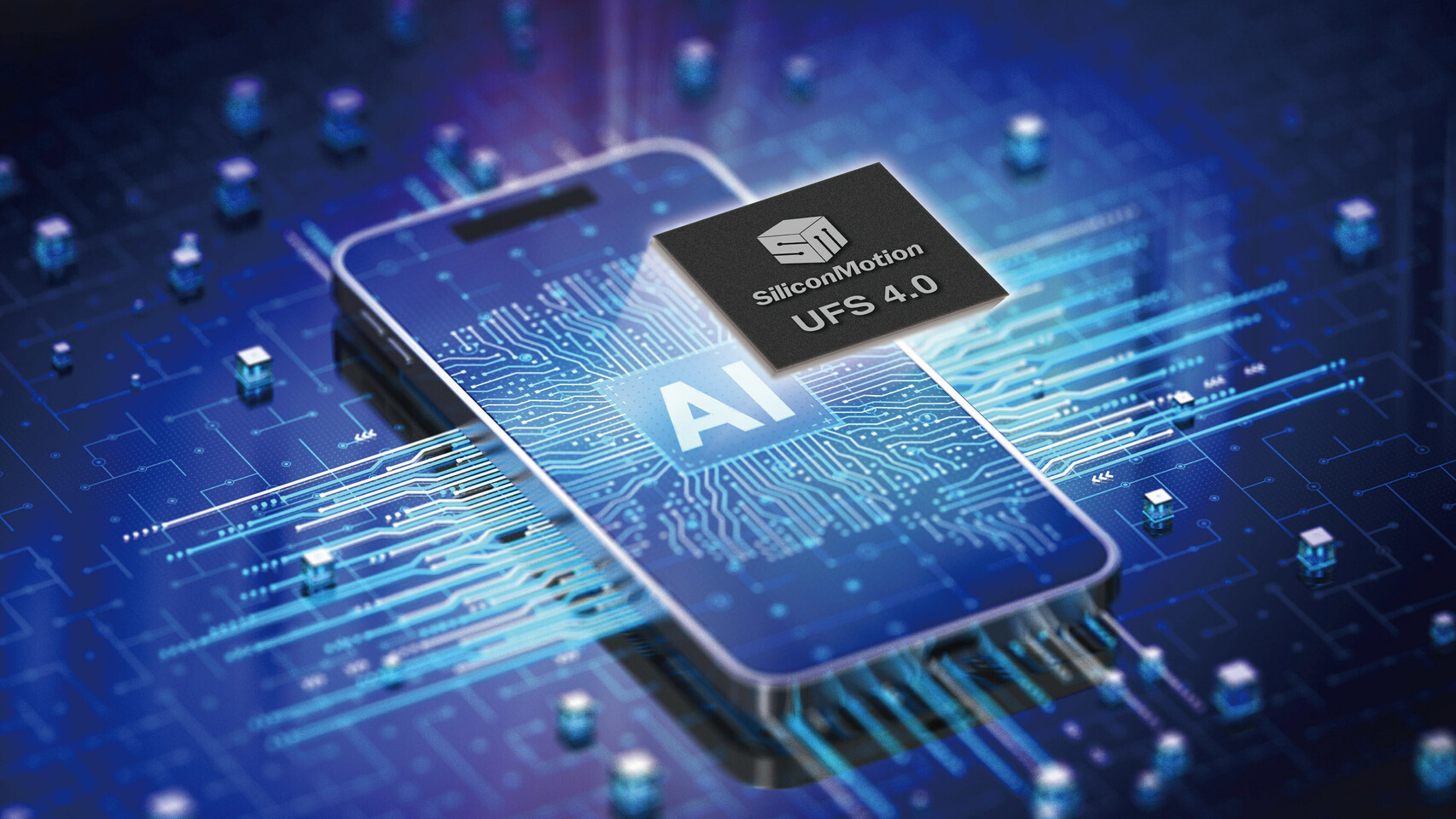
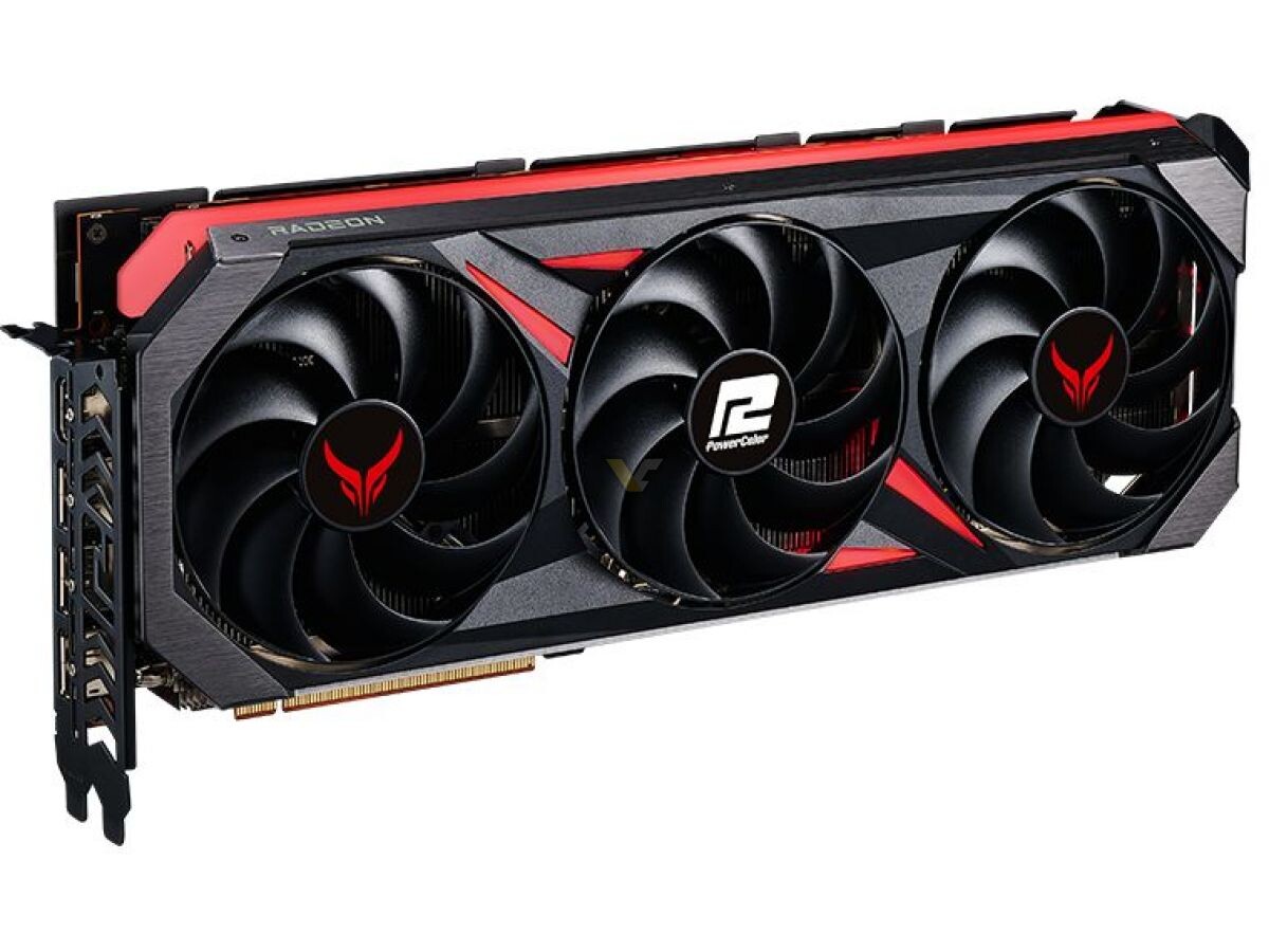
Silicon Motion Unveils 6nm UFS 4.0 Controller for AI Smartphones, Edge Computing and Automotive Applications

Silicon Motion Technology Corporation ("Silicon Motion"), a global leader in designing and marketing NAND flash controllers for solid state storage devices, today introduced its UFS (Universal Flash Storage) 4.0 controller, the SM2756, as the flagship of the industry's broadest merchant portfolio of UFS controller solutions for the growing requirements of AI-powered smartphones as well as other high-performance applications including automotive and edge computing. The company also added a new, second generation SM2753 UFS 3.1 controller to broaden its portfolio of controllers now supporting UFS 4.0 to UFS 2.2 standards. Silicon Motion's UFS portfolio delivers high-performance and low power embedded storage for flagship to mainstream and value mobile and computing devices, supporting the broadest range of NAND flash, including next-generation high speed 3D TLC and QLC NAND.

The new SM2756 UFS 4.0 controller solution is the world's most advanced controller, built on leading 6 nm EUV technology and using MIPI M-PHY low-power architecture, providing the right balance of high performance and power efficiency to enable the all day computing needs of today's premium and AI mobile devices. The SM2756 achieves sequential read performance exceeding 4,300 MB/s and sequential write speeds of over 4,000 MB/s and supports the broadest range of 3D TLC and QLC NAND flash with densities of up to 2 TB.

Fibocom Intros MediaTek-powered 5G RedCap Module FM330

Fibocom, a global leading provider of IoT (Internet of Things) wireless solutions and wireless communication modules, launches a new series of 5G RedCap module integrated with MediaTek's T300 5G modem, which is the world's first 6 nm radio frequency system-on-chip (RFSOC) single die solution for 5G RedCap. By integrating a single-core Arm Cortex-A3 processor in a significantly compact PCB area, the FM330 series are optimal solutions that offer extended coverage, increased network efficiency and device battery life for industry customers.

Compliant with 3GPP R17 standards, the FM330 series supports mainstream 5G frequency bands worldwide and is capable of reaching a maximum bandwidth of 20 MHz, thus ensuring the peak data rate of up to 227 Mbps downlink and 122 Mbps uplink, sufficient to meet the demand for 5G applications with less data throughput while balancing the power efficiency. In hardware design, it adopts the M.2form factor measured at 30x42mm benefiting from the unique RFSOC solution integrated with T300, in addition to the optimized antenna design in 1T2R, which significantly saves the PCB area. Moreover, FM330 series is pin-compatible with Fibocom LTE Cat 6 module FM101, easing the concerns for customers' migration from 4G to 5G. Furthermore, the module provides 64QAM/256QAM (optional) modulation scheme to greatly optimize the cost and size.

SolidRun Unveils Ryzen V3000 CX7 Com Module

SolidRun, a leading developer and manufacturer of high-performance System on Module (SOM) solutions, Single Board Computers (SBC) and network edge solutions, today announced the launch of its new Ryzen V3000 CX7 Com module, configurable with the 8-core/16-thread Ryzen Embedded V3C48 Processor. Boasting AMD's state-of-the-art 6 nm "Zen 3" architecture, this ultra-powerful embedded solution offers industry-leading performance and power efficiency. As SolidRun's first x86-based Com Express 7 module, the Ryzen V3000 CX7 Com module ushers in a new era of efficient, high-performance computing for a diverse range of networking and edge applications.

"Our new Ryzen V3000 CX7 Com module is an exciting addition to our CX7 product line as it represents a significant leap forward in embedded computing and offers unmatched performance and scalability for networking and edge applications," said Dr. Atai Ziv, CEO at SolidRun. "By leveraging the power of AMD's Ryzen Embedded V3000 processor, we are empowering developers to create innovative solutions that meet the evolving demands of modern embedded computing."

AMD Readies X870E Chipset to Launch Alongside First Ryzen 9000 "Granite Ridge" CPUs

AMD is readying the new 800-series motherboard chipset to launch alongside its next-generation Ryzen 9000 series "Granite Ridge" desktop processors that implement the "Zen 5" microarchitecture. The chipset family will be led by the AMD X870E, a successor to the current X670E. Since AMD isn't changing the CPU socket, and this is very much the same Socket AM5, the 800-series chipset will support not just "Granite Ridge" at launch, but also the Ryzen 7000 series "Raphael," and Ryzen 8000 series "Hawk Point." Moore's Law is Dead goes into the details of what sets the X870E apart from the current X670E, and it all has to do with USB4.

Apparently, motherboard manufacturers will be mandated to include 40 Gbps USB4 connectivity with AMD X870E, which essentially makes the chipset a 3-chip solution—two Promontory 21 bridge chips, and a discrete ASMedia ASM4242 USB4 host controller; although it's possible that AMD's QVL will allow other brands of USB4 controllers as they become available. The Ryzen 9000 series "Granite Ridge" are chiplet based processors just like the Ryzen 7000 "Raphael," and while the 4 nm "Zen 5" CCDs are new, the 6 nm client I/O die (cIOD) is largely carried over from "Raphael," with a few updates to its memory controller. DDR5-6400 will be the new AMD-recommended "sweetspot" speed; although AMD might get its motherboard vendors to support DDR5-8000 EXPO profiles with an FCLK of 2400 MHz, and a divider.

More AMD Ryzen 9000 "Zen 5" Desktop Processor Details Emerge

AMD is looking to debut its Ryzen 9000 series "Granite Ridge" desktop processors based on the "Zen 5" microarchitecture some time around May-June 2024, according to High Yield YT, a reliable source with AMD leaks. These processors will be built in the existing Socket AM5 package, and be compatible with all existing AMD 600 series chipset motherboards. It remains to be seen if AMD debuts a new line of motherboard chipsets. Almost all Socket AM5 motherboards come with the USB BIOS flashback feature, which means motherboards from even the earliest production batches that are in the retail channel, should be able to easily support the new processors.

AMD is giving its next-gen desktop processors the Ryzen 9000 series processor model numbering, as it used the Ryzen 8000 series for its recently announced Socket AM5 desktop APUs based on the "Hawk Point" monolithic silicon. "Granite Ridge" will be a chiplet-based processor, much like the Ryzen 7000 series "Raphael." In fact, it will even retain the same 6 nm client I/O die (cIOD) as "Raphael," with some possible revisions made to increase its native DDR5 memory frequency (up from the current DDR5-5200), and improve its memory overclocking capabilities. It's being reported that DDR5-6400 could be the new "sweetspot" memory speed for these processors, up from the current DDR5-6000.

AMD Radeon RX 7600 XT Launches with a Large 16 GB Memory

AMD Radeon RX 7600 XT went on sale today, at a starting price of $330. Designed for maxed out AAA gameplay at 1080p, this card can try its hands with 1440p gaming, at mid-thru-high settings; you can use features such as FSR 2, FSR 3 Frame Generation, the AMD Fluid Motion Frames feature that extends frame generation to any DirectX 11/12 game; as well as the HyperRX one-click performance enhancement that's part of the AMD Software control panel app. AMD had already maxed out all available shaders on the 6 nm "Navi 33" monolithic silicon, but has opted not to rope in the larger "Navi 32" chiplet GPU for the RX 7600 XT. Instead, it attempted to squeeze out the most performance possible from the "Navi 33," by dialing up clock speeds, power limits, and doubling the memory size.

You still get 32 compute units on the RX 7600 XT, which are worth 2,048 stream processors, 64 AI accelerators, 32 Ray accelerators, 128 TMUs, and 64 ROPs, but the 128-bit GDDR6 memory bus now drives 16 GB of memory running at the same 18 Gbps speed, yielding 288 GB/s of bandwidth. The GPU game clock has been increased to 2.47 GHz, up from 2.25 GHz on the RX 7600. The power limit has been increased from 165 W to 190 W on the RX 7600 XT; and implementing DisplayPort 2.1 has been made mandatory for board partners (they can't opt for the DisplayPort 1.4a like they could on the RX 7600). AMD claims that the 16 GB of video memory should come in handy for content creators, and those dabbling with generative AI.

We have three reviews of the Radeon RX 7600 XT for you today, so be sure to check them all out.

Sapphire Radeon RX 7600 XT Pulse | XFX Radeon RX 7600 XT Speedster QICK 309 | ASRock Radeon RX 7600 XT Steel Legend

AMD Announces the Radeon RX 7600 XT 16GB Graphics Card

AMD announced the new Radeon RX 7600 XT graphics card, bolstering its mid-range of 1080p class GPUs. The RX 7600 XT is designed for maxed out AAA gaming at 1080p, although it is very much possibly to play many of the titles at 1440p with fairly high settings. You can also take advantage of technologies such as FSR 3 frame generation in games that support it, AMD Fluid Motion Frames on nearly all DirectX 12 and DirectX 11 games; as well as the new expanded AMD HyperRX performance enhancement that engages a host of AMD innovations such as Radeon Super Resolution, Anti-Lag, and Radeon Boost, to achieve a target frame rate.

The Radeon RX 7600 XT is based on the same 6 nm "Navi 33" silicon, and the latest RDNA 3 graphics architecture, as the Radeon RX 7600. If you recall, the RX 7600 had maxed out all 32 CU on the silicon. To design the RX 7600 XT, AMD retained the "Navi 33," but doubled the memory size to 16 GB, and increased the clock speeds. The 16 GB of memory is deployed across the same 128-bit wide memory bus as the 8 GB is on the RX 7600. The memory speed is unchanged, too, at 18 Gbps GDDR6-effective; as is the resulting memory bandwidth, of 288 GB/s. There are two key changes—the GPU clock speeds and power limits.

AMD Close to Launching Radeon RX 7800M Series Based on "Navi 32"

AMD's small Radeon RX 7000M and RX 7000S lines of mobile GPUs based on the latest RDNA 3 graphics architecture includes just five SKUs, spanning the "Navi 31" and "Navi 33" chips. The RX 7000M series only has enthusiast-segment RX 7900M series based on the "Navi 31," and the RX 7600M series based on the "Navi 33," leaving a vast gap that the company plans to fill with RX 7800M series and RX 7700M series SKUs based on the "Navi 32," referred to internally as "Cuarzo Verde." The GPU is meant to be hardwired onto the mainboards of gaming notebooks, however, AMD hands out reference-design MXM boards to OEMs. These were sniffed out in a public shipping manifest harukaze5719 on Twitter.

The "Navi 32" package is roughly similar in size to the compacted "Navi 31" package powering the RX 7900M series. It has a physically smaller 5 nm GCD with 60 compute units compared to the 96 on the "Navi 31" GCD; and is surrounded by four 6 nm MCDs, which give it 64 MB of Infinity Cache, and a 256-bit GDDR6 memory bus. With this, AMD has the option of not just carving out RX 7800M series and RX 7700M series SKUs, but also RX 7900S series SKUs within its segment aimed at gaming-grade ultraportables. We could see some product announcements to this effect Q1 2024, alongside some new desktop SKUs.

MediaTek Expands Wi-Fi 7 Portfolio with New Chipsets for Mainstream Devices

MediaTek, one of the first adopters of Wi-Fi 7 technology, now has the industry's most comprehensive Wi-Fi 7 portfolio with today's introduction of the company's new Filogic 860 and Filogic 360 solutions. Together, these second-generation additions aim to further expand MediaTek's platform of cutting-edge products that utilize the latest technology advancements in connectivity while achieving peak performance and always-on reliability.

Filogic 860 combines a Wi-Fi 7 dual-band access point with a new advanced network processor solution and is ideal for enterprise access points, service provider Ethernet gateways and mesh nodes, as well as retail and IoT router applications. Filogic 360 is a stand-alone client solution that integrates Wi-Fi 7 2x2 and dual Bluetooth 5.4 radios in a single chip, and is designed to deliver next-generation Wi-Fi 7 connectivity to edge devices, streaming devices and a vast array of other consumer electronics.

AMD Mobile Processor Lineup in 2025 Sees "Fire Range," "Strix Halo," and Signficant AI Performance Increases

With Windows 11 23H2 setting the stage for increased prevalence of AI in client PC use cases, the new hardware battleground between AMD and its rivals Intel, Apple, and Qualcomm, will be in equipping their mobile processors with sufficient AI acceleration performance. AMD already introduced accelerated AI with the current "Phoenix" processor that debuts Ryzen AI, and its Xilinx XDNA hardware backend that provides a performance of up to 16 TOPS. This will see a 2-3 fold increase with the company's 2024-25 mobile processor lineup, according to a roadmap leak by "Moore's Law is Dead."

At the very top of the pile, in a product segment called "ultimate compute," which consists of large gaming notebooks, mobile workstations, and desktop-replacements; the company's current Ryzen 7045 "Dragon Range" processor will continue throughout 2024. Essentially a non-socketed version of the desktop "Raphael" MCM, "Dragon Range" features up to two 5 nm "Zen 4" CCDs for up to 16 cores, and a 6 nm cIOD. This processor lacks any form of AI acceleration. In 2025, the processor will be succeeded with "Fire Range," a similar non-socketed, mobile-friendly MCM that's derived from "Granite Ridge," with up to two 4 nm "Zen 5" CCDs for up to 16 cores; and the 6 nm cIOD. What's interesting to note here, is that the quasi-roadmap makes no mention of AI acceleration for "Fire Range," which means "Granite Ridge" could miss out on Ryzen AI acceleration from the processor. Modern discrete GPUs from both NVIDIA and AMD support AI accelerators, so this must have been AMD's consideration to exclude an XDNA-based Ryzen AI accelerator on "Fire Range" and "Granite Ridge."

Intel Launches Arc A580 Graphics Card for 1080p AAA Gaming at $179

Intel today launched the Arc A580 "Alchemist" desktop graphics card, with general availability across both the prebuilt and DIY retail channels. The card starts at a price of USD $179.99. The A580 targets the lower-end of the mid-range, and is targeted at AAA gaming at 1080p with medium-thru-high settings. The card fully meets DirectX 12 Ultimate feature-requirements, and is based on the Xe HPG "Alchemist" graphics architecture that powers the current Arc A750 and A770.

The new A580 has a lot in common with the Arc 7-series, as it is based on the same 6 nm ACM-G10 (aka DGX-512) silicon that powers them. Intel carved out this SKU by enabling 24 out of 32 Xe Cores, across 6 out of 8 Render Slices. This results in 384 execution units, or 3,072 unified shaders, 384 XMX AI acceleration cores, 24 Ray Tracing engines, 192 TMUs, and 96 ROPs. Perhaps the best aspect of the A580 is its memory sub-system that's been carried over from the A750—you get 8 GB of 16 Gbps GDDR6 memory across a 256-bit memory bus, yielding a segment-best 512 GB/s memory bandwidth. Intel claims that the Arc A580 should provide performance highly competitive to the GeForce RTX 3050, but there's more to this, do check out our reviews.

ASRock Arc A580 Challenger OC | Sparkle Arc A580 Orc

Lower Mainstream Graphics Segment Sees Action with Arc A580 and GeForce RTX 3050 6GB

The lower mainstream graphics segment is considered to be the starting point for PC gaming, targeting 1080p gaming with medium-thru-high (though not extreme) settings, and popular e-sports titles at 1080p with high settings. This segment is preparing to see some action in the coming days, with the introduction of two new products, the Intel Arc A580, and a new 6 GB variant of the GeForce RTX 3050. We've seen the A580 "Alchemist" in development for a while now.

Based on the 6 nm ACM-G12 silicon, the Arc A580 comes with 24 Xe Cores, or 384 EU (execution units), which work out to 3,072 unified shaders, compared to the 3,584 of the A750, 4,096 of the A770, and the significantly lower 1,024 of the entry-level A380. The most interesting aspect of the A580 is its memory. Although 8 GB in size, it uses a wide 256-bit memory interface, and 16 Gbps memory speed, which works out to a generous 512 GB/s of bandwidth. The A580 also comes with a full PCI-Express 4.0 x16 host interface.

Winbond Introduces Innovative CUBE Architecture for Powerful Edge AI Devices

Winbond Electronics Corporation, a leading global supplier of semiconductor memory solutions, has unveiled a powerful enabling technology for affordable Edge AI computing in mainstream use cases. The Company's new customized ultra-bandwidth elements (CUBE) enable memory technology to be optimized for seamless performance running generative AI on hybrid edge/cloud applications.

CUBE enhances the performance of front-end 3D structures such as chip on wafer (CoW) and wafer on wafer (WoW), as well as back-end 2.5D/3D chip on Si-interposer on substrate and fan-out solutions. Designed to meet the growing demands of edge AI computing devices, it is compatible with memory density from 256 Mb to 8 Gb with a single die, and it can also be 3D stacked to enhance bandwidth while reducing data transfer power consumption.

AMD EPYC 8004 "Siena" Processors with "Zen 4c" and New SP6 Platform Announced

AMD today rolled out the new compacted Socket SP6 server platform designed for smaller servers locally deployed at the edge by organizations. With CPU core-counts of up to 64-core/128-thread, these processors are based on the "Zen 4c" microarchitecture, which comes with identical IPC and ISA to "Zen 4," but with smaller L3 cache available per core. The EPYC 8004 series targets traditional data-centers located on-site for organizations. Even if the heavy-lifting of the IT for them is performed by remote data-centers or cloud providers, organizations still need smaller edge server deployments. The EPYC 8004 series caters to a different kind of servers than the ones the lower core-count models of EPYC 9004 "Genoa" do.

With the EPYC 8004 series, AMD is debuting a new smaller CPU socket called SP6. The socket measures 58.5 mm x 75.4 mm, compared to the 76.0 mm x 80.0 mm of Socket SP5 powering EPYC 9004 "Genoa" and EPYC 97x4 "Bergamo." Socket SP5 is an LGA with a pin count of 4,844, compared to SP5, which is LGA-6096. The first line of processors for this socket, the EPYC 8004 series, are codenamed "Siena." These are very much part of the 4th Gen EPYC series, a lineage it shares with "Genoa" for data-center servers, "Genoa-X" for compute servers, and "Bergamo" for high-density cloud.

Top Ten Semiconductor Foundries Report a 1.1% Quarterly Revenue Decline in 2Q23, Anticipated to Rebound in 3Q23

TrendForce reports an interesting shift in the electronics landscape: dwindling inventories for TV components, along with a surging mobile repair market that's been driving TDDI demand, have sparked a smattering of urgent orders in the Q2 supply chain. These last-minute orders have served as pivotal lifelines, propping up Q2 capacity utilization and revenue for semiconductor foundries. However, the adrenaline rush from these stop-gap orders may be a short-lived phenomenon and is unlikely to be carried over into the third quarter.

On the other hand, demand for staple consumer products like smartphones, PCs, and notebooks remains sluggish, perpetuating a slump in the use of expensive, cutting-edge manufacturing processes. At the same time, traditionally stable sectors—automotive, industrial control, and servers—are undergoing inventory correction. The confluence of these trends has resulted in a sustained contraction for the world's top ten semiconductor foundries. Their global revenue declined by approximately 1.1% for the quarter, amounting to a staggering US$26.2 billion.

AMD "Navi 4C" GPU Detailed: Shader Engines are their own Chiplets

"Navi 4C" is a future high-end GPU from AMD that will likely not see the light of day, as the company is pivoting away from the high-end GPU segment with its next RDNA4 generation. For AMD to continue investing in the development of this GPU, the gaming graphics card segment should have posted better sales, especially in the high-end, which it didn't. Moore's Law is Dead scored details of what could have been a fascinating technological endeavor for AMD, in building a highly disaggregated GPU.

AMD's current "Navi 31" GPU sees a disaggregation of the main logic components of the GPU that benefit from the latest 5 nm foundry node to be located in a central Graphics Compute Die; surrounded by up to six little chiplets built on the older 6 nm foundry node, which contain segments of the GPU's Infinity Cache memory, and its memory interface—hence the name memory cache die. With "Navi 4C," AMD had intended to further disaggregate the GPU, identifying even more components on the GCD that can be spun out into chiplets; as well as breaking up the shader engines themselves into smaller self-contained chiplets (smaller dies == greater yields and lower foundry costs).

AMD Radeon RX 7700 XT Confirmed with 192-bit Memory Bus in ASRock Regulatory Leak

AMD Radeon RX 7700 XT is confirmed to feature 12 GB as its standard memory size, and feature a 192-bit wide GDDR6 memory interface, according to a leaked regulatory filing by ASRock for its upcoming graphics cards. We already know from last week's mega leak of the PowerColor RX 7800 XT Red Devil that the card maxes out the "Navi 32" silicon, enabling all 60 RDNA3 CU, and comes with 16 GB of memory across the chip's full 256-bit memory bus. This filing suggests how AMD will carve the RX 7700 XT out.

Probably designed to compete with the GeForce RTX 4070, the RX 7700 XT is based on the same "Navi 32" silicon as the RX 7800 XT, but cut down. AMD is expected to disable some of the 60 CU physically present on the 5 nm GCD, while one of the four 6 nm MCDs will be disabled, giving the chip a 192-bit memory bus to drive its 12 GB of memory. We know from the PowerColor leak that the RX 7800 XT gets 18 Gbps memory speed. It remains to be seen if AMD sticks with this speed for even the RX 7700 XT, in which case, it gets 432 GB/s of memory bandwidth at its disposal. AMD is expected to launch the RX 7800 XT and RX 7700 XT within this quarter (before October).

PowerColor AMD Radeon RX 7800 XT Pictured, Confirmed Based on "Navi 32"

PowerColor inadvertently released the first pictures of its AMD Radeon RX 7800 XT Red Devil graphics card. These pictures confirm that the RX 7800 XT is based on a maxed out version of the "Navi 32" GPU, and not the compact "Navi 31" powering the limited edition RX 7900 GRE. The "Navi 32" is a chiplet-based GPU, just like the "Navi 31," albeit smaller. Its 5 nm GCD (graphics compute die) physically features 60 RDNA3 compute units, which work out to 3,840 stream processors, 120 AI accelerators, 60 Ray accelerators, 192 TMUs, and possibly 128 ROPs. This GCD is surrounded by four 6 nm MCDs (memory cache dies), which each has a 16 MB segment of the GPU's 64 MB Infinity Cache memory, and make up its 256-bit GDDR6 memory interface.

The specs sheet put out by PowerColor confirms that the RX 7800 XT maxes out the "Navi 32," enabling all 60 CUs, and the chip's full 256-bit memory interface, to drive 16 GB of memory. The RX 7800 XT uses 18 Gbps memory speed, and hence has 576 GB/s of memory bandwidth at its disposal. The PowerColor RX 7800 XT Red Devil has dual-BIOS, and assuming the "standard/silent" BIOS runs the card at AMD reference clock speeds, we're looking at Game clocks of 2210 MHz, and 2565 MHz boost. The Red Devil draws power from a dual 8-pin PCIe power connector set up (375 W max); the cooler is visibly smaller than the one on the company's RX 7900 series Red Devil cards. A 16+2 phase VRM powers the card. With pictures of the card out, we expect a global product launch within the next 30 days.

AMD Announces Radeon PRO W7600 and W7500 Graphics Cards

AMD today announced the Radeon PRO W7600 and W7500 graphics cards for the professional-visualization (pro-vis) market segment. These cards target the mid-range of the pro-vis segment, with segment price-band ranging between $350-950. The two are hence positioned below the W7800 and W7900 that the company launched in April. The W7600 and W7500 are based on the same RDNA3 graphics architecture as those two, and the client-segment RX 7000 series. AMD is pricing the the two new cards aggressively compared to NVIDIA. Both the W7500 and W7600 are based on the 6 nm "Navi 33" silicon.

The Radeon PRO W7600 leads today's launch, maxing out the silicon it is based on—you get 32 RDNA3 compute units, or 2,048 stream processors; 64 AI Accelerators, 32 Ray Accelerators; 128 TMUs, and 64 ROPs. The card comes with 8 GB of 18 Gbps GDDR6 memory across a 128-bit wide memory bus. The memory does not feature ECC. The card comes with a 130 W typical power draw, with a single 6-pin PCIe power connector. It uses a slick single-slot lateral-airflow cooling solution. AMD claims 20 TFLOPs peak FP32 performance.

Radeon RX 7900 GRE Confirmed to Debut New Navi 3X GPU

It turns out that the upcoming Radeon RX 7900 GRE (Golden Rabbit Edition) is built on the mysterious Navi 31 + Navi 32 hybrid GPU that's been in the news for a few weeks now. AMD has reportedly developed its answer to NVIDIA's AD103 silicon in the form of a new MCM that combines the 5 nm GCD of the "Navi 31," along with the substrate of the "Navi 32," which is physically smaller, and only has four 6 nm MCDs. This hybrid MCM could power AMD's mobile Radeon RX 7900 series. The chip physically only has a 256-bit wide GDDR6 memory interface. AMD felt the need for such a contraption as the "Navi 31" is likely too big for mobile platforms, and because the "Navi 32" GCD with its 60 CU (3,840 stream processors) might prove inadequate against a maxed out AD104 or cut-down AD103.

VideoCardz caught whiff of the new GPU by comparing the back sides of the Sapphire RX 7900 GRE from yesterday's leak, with that of the production Sapphire RX 7900 XT/XTX NITRO+. There are visible differences in the layout of the SMDs, and the reinforcement brace behind the GPU has a square cutout, compared to the rectangular one behind the "Navi 31" powering the RX 7900 XT/XTX NITRO+. On the RX 7900 GRE, the GCD is configured with 84 CU, or the same core-config as the RX 7900 XT, albeit with the narrower 256-bit memory interface, and 64 MB of Infinity Cache memory. It's highly likely that AMD uses this GPU to carve out the Radeon RX 7800 XT (with fewer than 84 but higher than 60 CU); while creating the RX 7800 with a maxed out "Navi 32," and the RX 7700 series with a cut-down "Navi 32" (including by narrowing the memory bus width to 192-bit by disabling one of the four MCDs). AMD is reportedly planning to launch the RX 7900 GRE in China, on July 28, 2023.

AMD Planning September Launch for Radeon RX 7800 series and RX 7700 series

AMD is planning to plug the Atlantic gap between its mainstream Radeon RX 7600 and enthusiast-class RX 7900 XT with the RX 7800 series and RX 7700 series, with either an announcement or teaser planned for 2023 Gamescom, which is scheduled for August. There could be up to four new graphics card SKUs announced, with their product launches spread across Q3 and Q4 2023. The "Navi 32" MCM is expected to power at least three of these SKUs, while it was recently rumored that AMD could design a new GPU that has the GCD of the "Navi 31" on the package of "Navi 32" with its four MCDs, to end up with a higher CU count than what the "Navi 32" can offer.

The "Navi 32" GPU is an MCM, just like the "Navi 31" powering the RX 7900 series. It is rumored to feature a 5 nm GCD (graphics compute die) with 60 RDNA3 compute units, which work out to 3,840 stream processors, 120 AI accelerators, 60 Ray Accelerators, 240 TMUs, and possibly 128 ROPs. The four 6 nm MCDs give it 64 MB of Infinity Cache, and a 256-bit wide GDDR6 memory interface. Assuming the RX 7800 XT uses the unnamed new MCM with the GCD of the "Navi 31" that has a CU count somewhere between 60 and 72, a maxed-out "Navi 32" could power the RX 7800, while its cut-down variants power the RX 7700 XT and RX 7700.

Radeon RX 7800 XT Based on New ASIC with Navi 31 GCD on Navi 32 Package?

AMD Radeon RX 7800 XT will be a much-needed performance-segment addition to the company's Radeon RX 7000-series, which has a massive performance gap between the enthusiast-class RX 7900 series, and the mainstream RX 7600. A report by "Moore's Law is Dead" makes a sensational claim that it is based on a whole new ASIC that's neither the "Navi 31" powering the RX 7900 series, nor the "Navi 32" designed for lower performance tiers, but something in between. This GPU will be AMD's answer to the "AD103." Apparently, the GPU features the same exact 350 mm² graphics compute die (GCD) as the "Navi 31," but on a smaller package resembling that of the "Navi 32." This large GCD is surrounded by four MCDs (memory cache dies), which amount to a 256-bit wide GDDR6 memory interface, and 64 MB of 2nd Gen Infinity Cache memory.

The GCD physically features 96 RDNA3 compute units, but AMD's product managers now have the ability to give the RX 7800 XT a much higher CU count than that of the "Navi 32," while being lower than that of the RX 7900 XT (which is configured with 84). It's rumored that the smaller "Navi 32" GCD tops out at 60 CU (3,840 stream processors), so the new ASIC will enable the RX 7800 XT to have a CU count anywhere between 60 to 84. The resulting RX 7800 XT could have an ASIC with a lower manufacturing cost than that of a theoretical Navi 31 with two disabled MCDs (>60 mm² of wasted 6 nm dies), and even if it ends up performing within 10% of the RX 7900 XT (and matching the GeForce RTX 4070 Ti in the process), it would do so with better pricing headroom. The same ASIC could even power mobile RX 7900 series, where the smaller package and narrower memory bus will conserve precious PCB footprint.

Top 10 Foundries Report Nearly 20% QoQ Revenue Decline in 1Q23, Continued Slide Expected in Q2

TrendForce reports that the global top 10 foundries witnessed a significant 18.6% QoQ decline in revenue during the first quarter of 2023. This decline—amounting to approximately US$27.3 billion—can be attributed to sustained weak end-market demand and the compounded effects of the off-peak season. The rankings also underwent notable changes, with GlobalFoundries surpassing UMC to secure the third position, and Tower Semiconductor surpassing PSMC and VIS to claim the seventh spot.

Declining capacity utilization rate and shipment volume contribute to widened revenue decline
The revenue decline in Q1 was primarily influenced by declining capacity utilization rates and shipment volume across the top 10 foundries. For instance, TSMC generated US$16.74 billion in revenue—marking a 16.2% QoQ drop in revenue. Weakened demand for mainstream applications such as laptops and smartphones led to a significant decline in the utilization rates and revenue of the 7/6 nm and 5/4 nm processes, falling over 20% and 17%, respectively. While the second quarter may see temporary relief coming from rush orders, the persistently low capacity utilization rate indicates that revenue is likely to continue declining, albeit at a slower pace compared to Q1.

AMD EPYC "Bergamo" Uses 16-core Zen 4c CCDs, Barely 10% Larger than Regular Zen 4 CCDs

A SemiAnalysis report sheds light on just how much smaller the "Zen 4c" CPU core is compared to the regular "Zen 4." AMD's upcoming high core-count enterprise processor for cloud data-center deployments, the EPYC "Bergamo," is based on the new "Zen 4c" microarchitecture. Although with the same ISA as "Zen 4," the "Zen 4c" is essentially a low-power, lite version of the core, with significantly higher performance/Watt. The core is physically smaller than a regular "Zen 4" core, which allows AMD to create CCDs (CPU core dies) with 16 cores, compared to the current "Zen 4" CCD with 8.

The 16-core "Zen 4c" CCD is built on the same 5 nm EUV foundry node as the 8-core "Zen 4" CCD, and internally features two CCX (CPU core complex), each with 8 "Zen 4c" cores. Each of the two CCX shares a 16 MB L3 cache among the cores. The SemiAnalysis report states that the dedicated L2 cache size of the "Zen 4c" core remains at 1 MB, just like that of the regular "Zen 4." Perhaps the biggest finding is their die-size estimation, which puts the 16-core "Zen 4c" CCD just 9.6% larger in die-area, than the 8-core "Zen 4" CCD. That's 72.7 mm² per CCD, compared to 66.3 mm² of the regular 8-core "Zen 4" CCD.

ASRock AMD Radeon RX 7600 Custom Card Already Discounted in Spain

AMD and its board partners have finally debuted Radeon RX 7600 graphics cards this week, and hardware enthusiasts were somewhat pleased about Team Red's last minute adjustment to the lineup's MSRP - rumors had to pointed to an expected $299 base price, but the monolithic RDNA 3 Navi 33 XL GPU (6 nm) card hit the market with a starting SEP of $269/€299.99. Buyer perception is difficult to gauge, but recent GPU product launches have indicated that folks are simply not rushing to the store to pick up the latest and greatest from AMD and NVIDIA alike.

A major Spanish e-tailer, CoolMod, is reported to be the first European store to offer a custom Radeon RX 7600 card at a discounted price of €259.94 ($279) which includes VAT - having adjusted the figure a mere day after the official launch - resulting in a saving of €40 (13% reduction). The ASRock Challenger OC 8 GB model was announced yesterday, alongside its Steel Legend and Phantom Gaming siblings - the latter has been reviewed by TPU's W1zzard. His assessment concludes: "At its price point, the RX 7600 offers virtually the same price/performance as the RX 6600 XT ($250), which makes it a tough sale, especially when you factor in price increases for custom designs. While AMD does have some technological improvements like HDMI 2.1, DisplayPort 2.1 and AV1 video encode/decode, I think none of these are relevant in this segment, at least not to the majority of potential customers; NVIDIA has the DLSS 3 carrot to dangle in front of gamers. The RX 7600 should really be $199 or $229 to make it an interesting option."
Return to Keyword Browsing
May 1st, 2024 06:37 EDT change timezone

New Forum Posts

Popular Reviews

Controversial News Posts