News Posts matching #7 nm

Return to Keyword Browsing

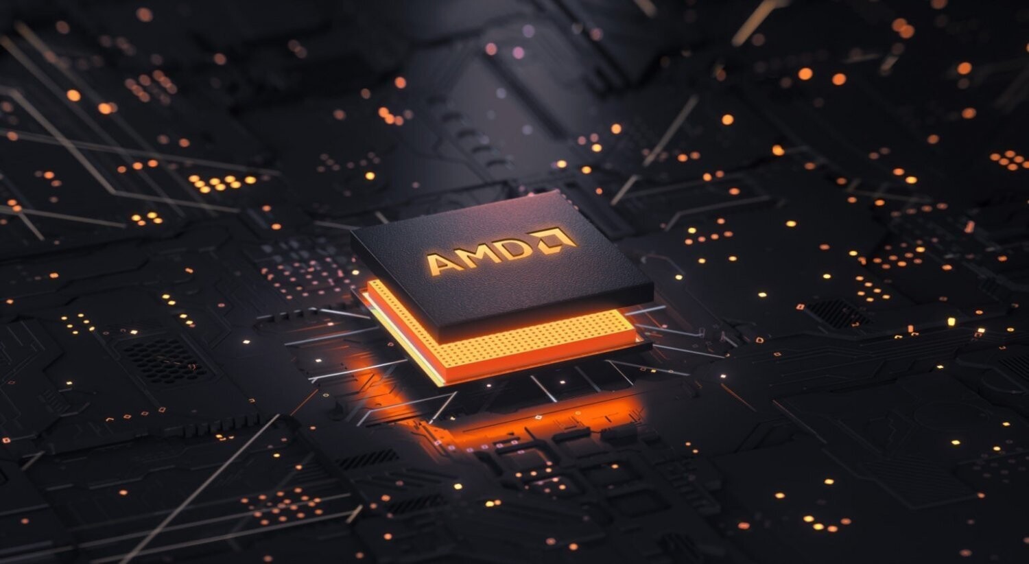
Intel CEO Says Using Competitor's Semiconductor Process in Intel Fabs is an Option

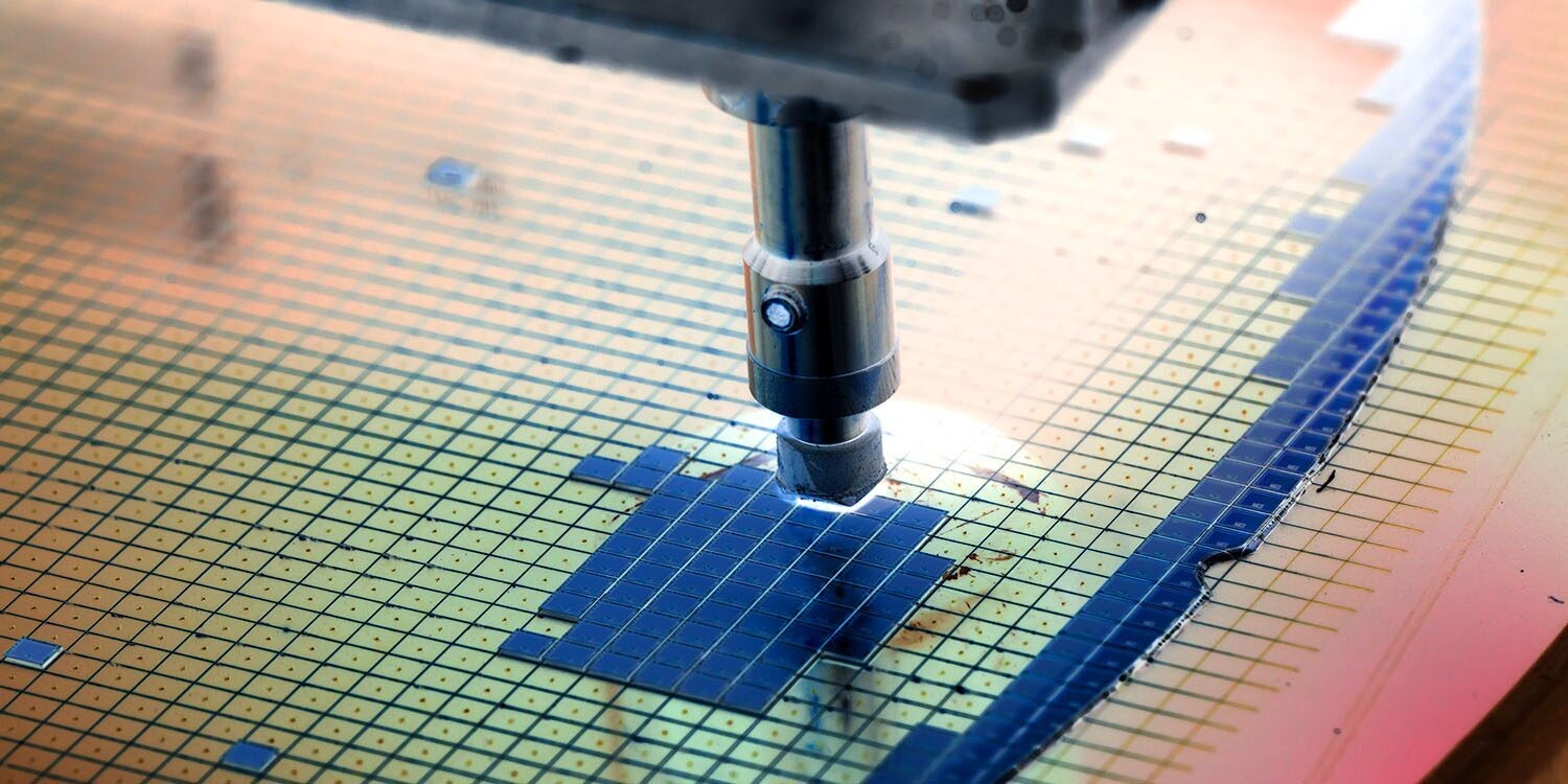
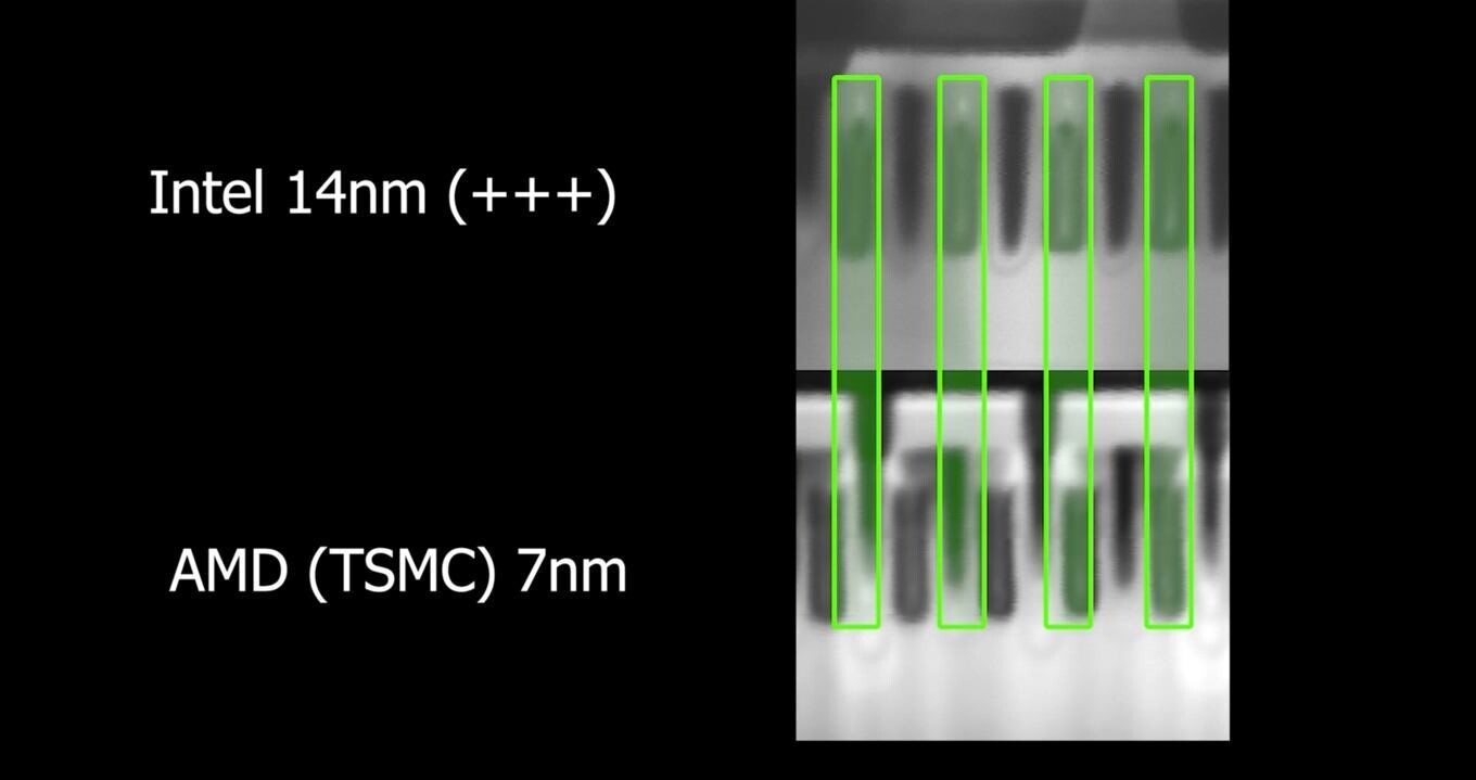
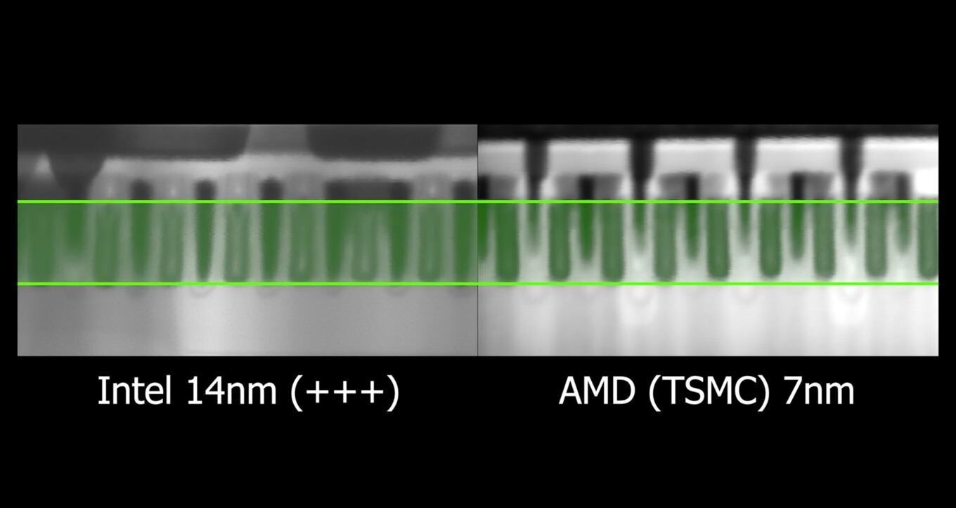
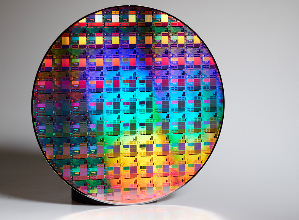
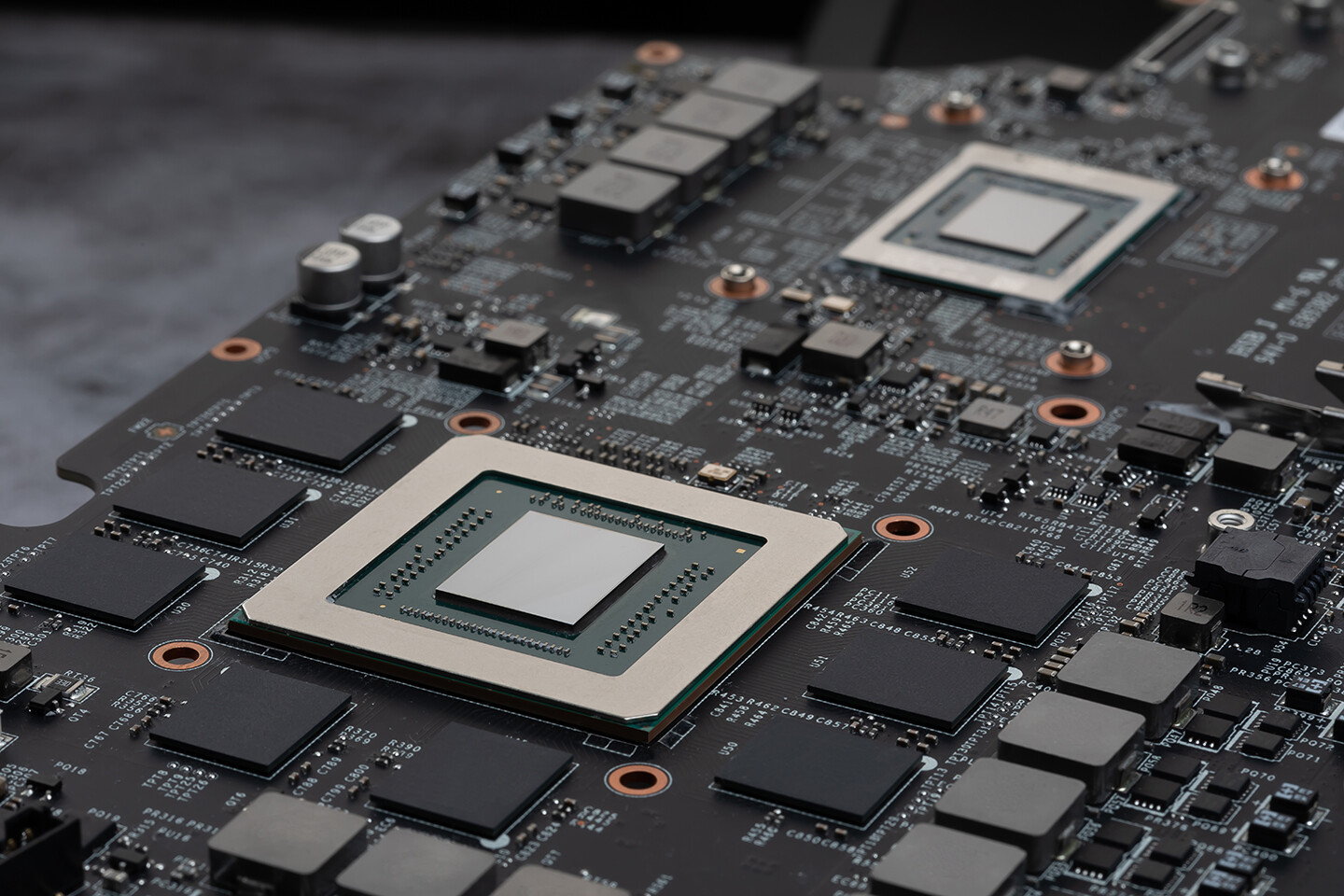
Semiconductor manufacturing is not an easy feat to achieve. Especially if you are constantly chasing the smaller and smaller node. Intel knows this the best. The company has had a smooth transition from other nodes to the smaller ones until the 10 nm node came up. It has brought Intel years of additional delay and tons of cost improving the yields of a node that was seeming broken. Yesterday the company announced the new Tiger Lake-H processors for laptops that are built using the 10 nm process, however, we are questioning whatever Intel can keep up with the semiconductor industry and deliver the newest nodes on time, and with ease. During an interview with Intel's CEO Bob Swan, we can get a glimpse of Intel's plans for the future of semiconductors at the company.

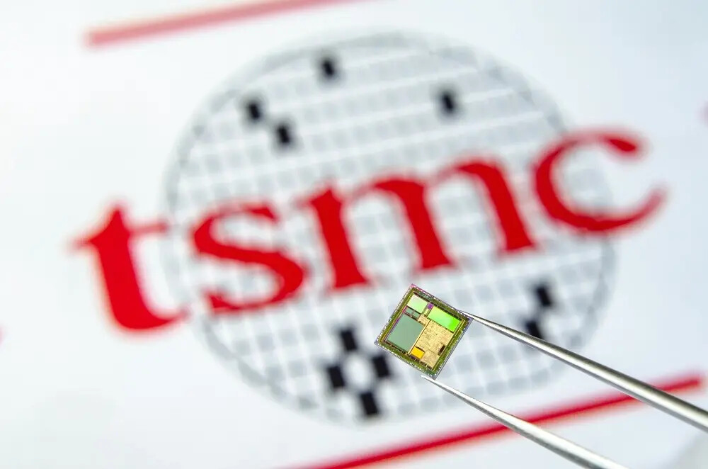
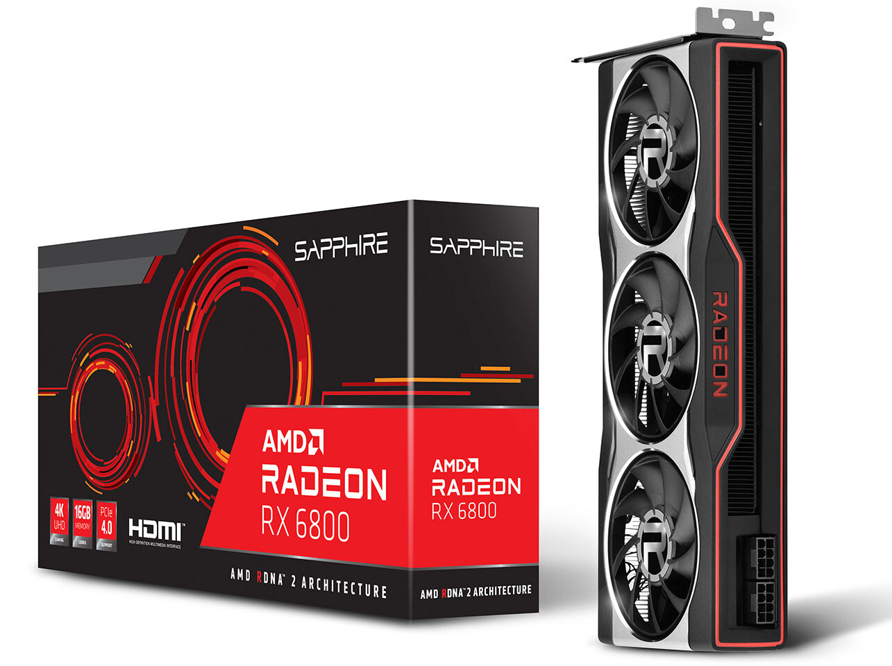
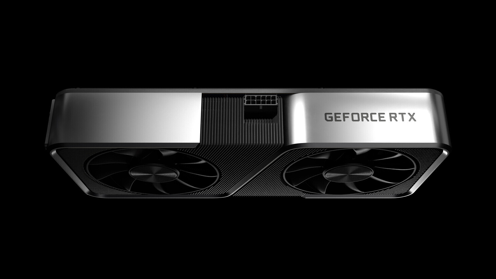
In the interview, Mr. Swan has spoken about the technical side of Intel and how the company plans to utilize its Fabs. The first question everyone was wondering was about the state of 10 nm. The node is doing well as three Fabs are ramping up capacity every day, and more products are expected to arrive on that node. Mr. Swan has also talked about outsourcing chip production, to which he responded by outlining the advantage Intel has with its Fabs. He said that outsourcing is what is giving us shortages like AMD and NVIDIA experience, and Intel had much less problems. Additionally, Mr. Swan was asked about the feasibility of new node development. To that, he responded that there is a possibility that Intel could license its competitor's node and produce it in their Fabs.

AMD 32-Core EPYC "Milan" Zen 3 CPU Fights Dual Xeon 28-Core Processors

AMD is expected to announce its upcoming EPYC lineup of processors for server applications based on the new Zen 3 architecture. Codenamed "Milan", AMD is continuing the use of Italian cities as codenames for its processors. Being based on the new Zen 3 core, Milan is expected to bring big improvements over the existing EPYC "Rome" design. Bringing a refined 7 nm+ process, the new EPYC Milan CPUs are going to feature better frequencies, which are getting paired with high core counts. If you are wondering how Zen 3 would look like in server configuration, look no further because we have the upcoming AMD EPYC 7543 32-core processor benchmarked in Geekbench 4 benchmark.

The new EPYC 7543 CPU is a 32 core, 64 thread design with a base clock of 2.8 GHz, and a boost frequency of 3.7 GHz. The caches on this CPU are big, and there is a total of 2048 KB (32 times 32 KB for instruction cache and 32 times 32 KB for data cache) of L1 cache, 16 MB of L2 cache, and as much as 256 MB of L3. In the GB4 test, a single-core test produced 6065 points, while the multi-core run resulted in 111379 points. If you are wondering how that fairs against something like top-end Intel Xeon Platinum 8280 Cascade Lake 28-core CPU, the new EPYC Milan 7543 CPU is capable of fighting two of them at the same time. In a single-core test, the Intel Xeon configuration scores 5048 points, showing that the new Milan CPU has 20% higher single-core performance, while the multi-core score of the dual Xeon setup is 117171 points, which is 5% faster than AMD CPU. The reason for the higher multi-core score is the sheer number of cores that a dual-CPU configuration offers (32 cores vs 56 cores).

AMD's Radeon RX 6700 Series Reportedly Launches in March

AMD may be finding itself riding a new wave of success caused by its accomplishments with the Zen architecture, which in turn bolstered its available R&D for its graphics division and thus turned the entire AMD business on its head. However, success comes at a cost, particularly when you don't own your own fabs and have to vie for capacity with TSMC against its cadre of other clients. I imagine that currently, AMD's HQ has a direct system of levers and pulleys that manage its chip allocation with TSMC: pull this lever and increase number of 7 nm SOC for the next-generation consoles; another controls Ryzen 5000 series; and so on and so on. As we know, production capacity on TSMC's 7 nm is through the roof, and AMD is finding it hard to ship enough of its Zen 3 CPUs and RDNA2 graphics cards. The reported delay for the AMD RX 6700 series may well be a result of AMD overextending its product portfolio on the 7 nm process with foundry partner TSMC.

A report coming from Cowcotland now points towards a 1Q2021 release for AMD's high-performance RX 6700 series, which was initially poised to see the light of day in the current month of January. The RX 6700 series will ship with AMD's Navi 22 chip, which is estimated to be half of the full Navi 21 chip (which puts it at a top configuration of 2560 Stream Processors over 40 CUs). These cards are expected to ship with 12 GB of GDDR6 memory over a 192-bit memory bus. However, it seems that AMD may have delayed the launch for these graphics cards. One can imagine that this move from AMD happens so as to not further dilute the TSMC wafers coming out of the factory, limited as they are, between yet another chip. One which will undoubtedly have lower margins than the company's Zen 3 CPUs, EPYC CPUs, RX 6800 and RX 6900, and that doesn't have the same level of impact on its business relations as console-bound SoCs. Besides, it likely serves AMD best to put out enough of its currently-launched products' to sate demand (RX 6000 series, Ryzen 5000, cof cof) than to launch yet another product with likely too limited availability in relation to the existing demand.

TSMC Ends Its Volume Discounts For the Biggest Customers, Could Drive Product Prices Up

Taiwan Semiconductor Manufacturing Company (TSMC), one of the largest semiconductor manufacturers in the world, is reportedly ending its volume discounts. The company is the maker of the currently smallest manufacturing nodes, like 7 nm and 5 nm. For its biggest customers, TSMC used to offer a discount - when you purchase 10s or 100s of thousands of 300 mm (12-inch) wafers per month, the company will give you a deal of a 3% price decrease per wafer, meaning that the customer is taking a higher margin off a product it sells. Many of the customers, like Apple, NVIDIA, and AMD, were a part of this deal.

Today, thanks to a report from the Taiwanese Central News Agency, TSMC is terminating this type of discount. Now, every customer will pay full price for the wafer, without any exceptions. For now, it is unclear what drove that decision at TSMC's headquarters, but the only thing that we could think is that the demand is too high to keep up with the discounts and the margins are possibly lower. What this means for consumers is a possible price increase in products that are manufactured at TSMC's facilities. The consumer market is already at a drought of new PC components like CPUs and GPUs due to high demand and scalping. This could contribute a bit to the issue, however, we do not expect it to be of any major significance.

Largest Swiss Retailer Digitec to Receive a Grand Total of 35 AMD RX 6900 XT Graphics Cards for Launch

AMD's launch of their top of the line RX 6900 XT graphics card seems that it will have even less availability than the company's high-end RX 6800 and RX 6800 XT graphics card. This isn't surprising; the RX 6900 XT is a 590 mm² beast of a GPU with all of its execution units enabled - that's a lot of die space to harvest without a single silicon fault, no matter how good TSMC's 7 nm manufacturing process really is. Stock will be scarce, and likely will be scarce throughout the lifetime of the product, especially with the clogged, unmet, existing demand for high performance GPUs from a world population that has turned to gaming as a solace in times of quarantine.

Digitec, the largest Swiss retailer (serving a population of 8.5 million people), is only receiving 35 RX 6900 XT graphics cards for launch. We don't know, of course, what exactly is the Swiss demand for high-performance graphics cards, but it being one of the world's wealthiest countries (when it comes to its population's average income) it's expected to be higher than other countries with comparable population but lower income. As a result, the retailer isn't even putting the cards up for sale as they normally would; instead, there's a sweepstakes of sorts where 35 random users that opt-in for the event will receive a code that allows them to purchase the graphics card for its retail price of $999. An interesting solution, albeit of course, it just signals the dimension of the cards' availability issues.

AWS Implements High-Performance EPYC and Radeon Pro Processors for Graphics Optimized Workloads

AMD announced Amazon Web Services, Inc. (AWS) has expanded its AMD-based offerings with a new cloud instance for Amazon Elastic Compute Cloud (Amazon EC2): Amazon EC2 G4ad instances for graphics-optimized workloads. With this new instance, AMD now powers eight Amazon EC2 instance families across 20 global AWS Regions. AMD also announced that Amazon GameLift, a fully managed dedicated game server hosting solution, is now providing its video game hosting customers access to AMD EPYC processor-based Amazon EC2 C5a, M5a and R5a instances.

"Today we build on the strong collaboration between AMD and AWS, which started in 2017. This expansion of our cooperation is a proof point of the continued performance and capabilities that AMD provides its customers," said Forrest Norrod, senior vice president and general manager, Data Center and Embedded Solutions Group, AMD. "Amazon EC2 G4ad instances are the first powered by both AMD EPYC CPUs and Radeon Pro GPUs, and adding to the existing EPYC processor-based instances, they exemplify the ways in which AMD CPUs and GPUs provide fantastic performance and price/performance for AWS customers."

"The high-performance capabilities of the AMD EPYC CPUs and Radeon Pro GPUs are enabling AWS to create a new graphics-focused instance that help us keep our leadership price/performance offerings that our customers expect," said David Brown, Vice President, Amazon EC2, Amazon Web Services, Inc. "We're delighted to continue this great collaboration with AMD, enabling the Amazon EC2 G4ad instances to provide the industry's best price performance for graphics-intensive applications."

ASRock Announces its Radeon RX 6800 XT and RX 6800 Series Custom-design Graphics Cards

The global leading motherboard manufacturer, ASRock, launched its AMD Radeon RX 6800 series graphics cards, including Taichi, Phantom Gaming, and the Challenger product series. From the high-end Radeon RX 6800 XT Taichi X 16G OC, the mid-level Radeon RX 6800 XT Phantom Gaming D 16G OC and Radeon RX 6800 Phantom Gaming D 16G OC, to the mainstream Radeon RX 6800 Challenger Pro 16G OC, the complete product line gives users the most variety of choices.

ASRock's AMD Radeon RX 6800 series graphics cards leverage 7 nm process technology and AMD RDNA 2 gaming architecture, and support the DirectX 12 Ultimate software standard and hardware-accelerated raytracing. The product line features 16 GB of 256-bit GDDR6 memory, and also supports the latest PCI Express 4.0 bus standard. It adopts ASRock's custom "Striped Axial Fan" and Polychrome SYNC ARGB LEDs, with outstanding pre-overclocked GPU clock settings and rich additional features. The performance of ASRock's AMD Radeon RX 6800 series graphics cards provide gamers with an excellent 4K gaming experience.

AMD Unveils Ryzen Embedded V2000 Processors with Enhanced Performance and Efficiency

AMD today launched a new product in its high-performance Embedded processor family, the AMD Ryzen Embedded V2000 Series processor. Built on the innovative 7 nm process technology, "Zen 2" cores and high-performance AMD Radeon graphics, the AMD Ryzen Embedded V2000 Series provides a new class of performance with 7 nm technology, incredible power efficiency and continues to deliver enterprise-class security features for embedded customers.

The AMD Embedded Ryzen V2000 family is designed for embedded applications such as Thin Client, MiniPC and Edge systems. Equipped with up to eight CPU cores and seven GPU compute units, a single AMD Ryzen Embedded V2000 Series processor provides 2x the multi-threaded performance-per-watt, up to 30 percent better single-thread CPU performance and up to 40 percent better graphics performance over the previous generation. For customers and applications that need high-performance display capabilities, the Ryzen Embedded V2000 series can power up to four independent displays in 4K resolution.

MediaTek Announces Dimensity 700 SoC For Mass Market 5G Smartphones

MediaTek today unveiled its new Dimensity 700 5G smartphone chipset, a 7 nm SoC designed to bring advanced 5G capabilities and experiences to the mass market. The addition of the Dimensity 700 to MediaTek's Dimensity family of 5G chips gives device makers a full suite of options for 5G smartphone models - from flagship and premium to mid-range and mass market devices - making 5G more accessible for consumers everywhere.

"With our expanded Dimensity portfolio we're bringing the latest 5G capabilities to every smartphone tier so more people can enjoy 5G experiences," said Dr. JC Hsu, Corporate VP and GM of MediaTek's Wireless Communications Business Unit. "The Dimensity 700 has an impressive mix of 5G connectivity features, advanced camera capabilities like night shot enhancements and multiple voice assistant support, all in a super power-efficient design."

Samsung's 5 nm Node in Production, First SoCs to Arrive Soon

During its Q3 earnings call, Samsung Electronics has provided everyone with an update on its foundry and node production development. In the past year or so, Samsung's foundry has been a producer of a 7 nm LPP (Low Power Performance) node as its smallest node. That is now changed as Samsung has started the production of the 5 nm LPE (Low Power Early) semiconductor manufacturing node. In the past, we have reported that the company struggled with yields of its 5 nm process, however, that seems to be ironed out and now the node is in full production. To contribute to the statement that the new node is doing well, we also recently reported that Samsung will be the sole manufacturer of Qualcomm Snapdragon 875 5G SoC.

The new 5 nm semiconductor node is a marginal improvement over the past 7 nm node. It features a 10% performance improvement that is taking the same power and chip complexity or a 20% power reduction of the same processor clocks and design. When it comes to density, the company advertises the node with x1.33 times increase in transistor density compared to the previous node. The 5LPE node is manufactured using the Extreme Ultra-Violet (EUV) methodology and its FinFET transistors feature new characteristics like Smart Difusion Break isolation, flexible contact placement, and single-fin devices for low power applications. The node is design-rule compatible with the previous 7 nm LPP node, so the existing IP can be used and manufactured on this new process. That means that this is not a brand new process but rather an enhancement. First products are set to arrive with the next generation of smartphone SoCs, like the aforementioned Qualcomm Snapdragon 875.

Sapphire Unveils Reference-design Radeon RX 6800 XT and RX 6800

Unlike NVIDIA, AMD still relies on its add-in board (AIB) partners to sell reference design (made by AMD) graphics cards, and Sapphire just announced its lineup. The company unveiled its reference-design Radeon RX 6800 XT and RX 6800 cards. The RX 6800 XT is characterized by its triple-slot cooling solution, while the RX 6800 makes do with a slimmer dual-slot one. Both cards are based on the 7 nm "Navi 21" silicon and feature 16 GB of 16 Gbps GDDR6 memory over a 256-bit wide memory interface, cushioned by 128 MB of on-die Infinity Cache.

The RX 6800 XT is configured with 72 out of 80 RDNA2 compute units on the "Navi 21" silicon, working out to 4,608 stream processors, 72 ray accelerators, 288 TMUs, and 128 ROPs. The engine clock of the RX 6800 XT boosts up to 2.25 GHz. The RX 6800, on the other hand, features 60 out of 80 RDNA2 compute units, which make up 3,840 stream processors, 60 ray accelerators, 240 TMUs, the same 128 ROPs, and the same memory subsystem as the RX 6800 XT. Given that these are reference cards, Sapphire could price them at AMD's baseline, with the RX 6800 XT going for $649, and the RX 6800 at $579.

Raja Koduri to Present at Samsung Foundry Forum amid Intel's Outsourcing Efforts

Intel's chief architect and senior vice president of discrete graphics division, Mr. Raja Koduri, is said to be scheduled to present at Samsung Electronics Event day. With a presentation titled "1000X More Compute for AI by 2025", the event is called Samsung Foundry SAFE Forum. It is a global virtual conference designed to be available to everyone. So you might be wondering what is Mr. Koduri doing there. Unless you have been living under a rock, you know about Intel's struggles with node manufacturing. Specifically, the 10 nm node delays that show the company's efforts to deliver a node on time. The same is happening with the 7 nm node that also experienced significant delays.

Intel has a contract to develop an exascale supercomputer at Argonne National Laboratory, called Aurora. That supercomputer is using Intel's CPUs and the company's upcoming Xe GPUs. Since the company has problems with manufacturing and has to deliver the products (it is bound by several contracts) to its contractors and customers, it decided to look at external manufacturers for its products, specifically Xe graphics. Being that Mr. Koduri tweeted an image of him visiting Samsung Giheung Fab in Korea, and now presenting at the Samsung Foundry event, it is possible that Intel will tap Samsung's semiconductor manufacturing process for its Xe GPU efforts and that Samsung will be the contractor in charge.

AMD Radeon RX 6000 Series Specs Leak: RX 6900 XT, RX 6800 XT, RX 6700 Series

AMD's Radeon RX 6000 series graphics cards, based on the RDNA2 graphics architecture, will see the introduction of the company's first DirectX 12 Ultimate graphics cards (featuring features such as real-time raytracing). A VideoCardz report sheds light on the specifications. The 7 nm "Navi 21" and "Navi 22" chips will power the top-end of the lineup. The flagship part is the Radeon RX 6900 XT, followed by the RX 6800 XT and RX 6800; which are all based on the "Navi 21." These are followed by the RX 6700 XT and RX 6700, which are based on the "Navi 22" silicon.

The "Navi 21" silicon physically features 80 RDNA2 compute units, working out to 5,120 stream processors. The RX 6900 XT maxes the chip out, enabling all 80 CUs, and is internally referred to as the "Navi 21 XTX." Besides these, the RX 6900 XT features 16 GB of GDDR6 memory across a 256-bit wide memory interface, and engine clocks boosting beyond 2.30 GHz. The next SKU in AMD's product stack is the RX 6800 XT (Navi 21 XT), featuring 72 out of 80 CUs, working out to 4,608 stream processors, the same 16 GB 256-bit GDDR6 memory configuration as the flagship, while its engine clocks go up to 2.25 GHz.

China's SMIC Announces N+1 Node Tape-Out for 7 nm Silicon

SMIC is taking immense strides in bridging the gap between China's in-house silicon manufacturing capability compared to the usual Taiwanese or US-based options. Despite its ties to the Chinese government, which led for a US blacklisting of the company amidst the current China-US trade-war, SMIC has definitely achieved a benchmark with its 7 nm tape-out. This was achieved after a number of funding rounds, some of them with the power of the Chinese state behind them. While the blacklisting definitely hurt the company, they still have access to ASML's semiconductor manufacturing equipment, so while the rope may be tight, it likely isn't suffocating.

The node's first production tape-out is for an ASIC (Application-Specific Integrated Circuit) design for Innosilicon, which specializes in cryptocurrency mining, purpose-built chips. SMIC states that the new N+1 process can offer up to 20% boosted performance at the same clocks and core complexity compared to their 12 nm designs, which is subpar compared to other player's "7 nm class nodes", such as GloFo's 12 LP+, Samsung's 8LPP and TSMC's N7 non-EUV nodes (TSMC, for instance, offered a 20% performance boost between the 10 nm and 7 nm nodes). SMIC's manufacturing looks better in other metrics, though: power requirements can be reduced by 57% at the same TDP and complexity, and the transistor density can be increased by up to 2.7 times, (the "up to" depends on specific semiconductor structures). This is SMIC is only targeting - for now - low-power and low-cost devices with the N+1 nodes.

NVIDIA Reportedly Moving Ampere to 7 nm TSMC in 2021

A report straight from DigiTimes claims that NVIDIA is looking to upgrade their Ampere consumer GPUs from Samsung's 8 nm to TSMC's 7 nm. According to the source, the volume of this transition should be "very large", but most likely wouldn't reflect the entirety of Ampere's consumer-facing product stack. The report claims that TSMC has become more "friendly" to NVIDIA. This could be because TSMC now has available manufacturing capacity in 7 nm due to some of its clients moving to the company's 5 nm node, or simply because TSMC hadn't believed NVIDIA to consider Samsung as a viable foundry alternative - which it now does - and has thus lowered pricing.

There are various reasons being leveraged at this, none with substantial grounds other than "reported from industry sources". NVIDIA looking for better yields is one of the appointed reasons, as is its history as a TSMC customer. NVIDIA shouldn't have too high a cost porting its manufacturing to TSMC in terms of design changes to the silicon level so as to cater to different characteristics of TSMC's 7 nm, because the company's GA100 GPU (Ampere for the non-consumer market) is already manufactured at TSMC. The next part of this post is mere (relatively informed) speculation, so take that with a saltier disposition than what came before.

AMD Ryzen 5000 "Zen 3" "Vermeer" Launch Liveblog

AMD is announcing its next-generation Ryzen 5000 series desktop processors in the Socket AM4 package. These 7 nm processors see the implementation of the company's new "Zen 3" microarchitecture, and are expected to push the performance envelope. AMD CEO Dr Lisa Su takes centerstage in a pre-recorded launch event stream which we are live-blogging. These are facts as they appear, along with our analysis.

Update 16:01 UTC: Looks like this is a pre-recorded stream made to look live (a premiere).

Intel Starts Hardware Enablement of Meteor Lake 7 nm Architecture

In a report by Phoronix, we have the latest information about Intel's efforts to prepare the next generation of hardware for launch sometime in the future. In the latest Linux kernel patches prepared to go mainline soon, Intel has been adding support for its "Meteor Lake" processor architecture manufactured on Intel's most advanced 7 nm node. While there are no official patches in the mainline kernel yet, the first signs of Meteor Lake are expected to show up in the version 5.10, where we will be seeing the mentions of it. This way Intel is ensuring that the Meteor Lake platform will see the best software support, even though it is a few years away from the launch.

Meteor Lake is expected to debut in late 2022 or 2023, which will replace the Alder Lake platform coming soon. In a similar way to Alder Lake, Meteor Lake will use a hybrid core technology where it will combine small and big cores. The Meteor Lake platform will use the new big "Ocean Cove" design paired with small "Gracemont" cores that will be powering the CPU. This processor is going to be manufactured on Intel's 7 nm node that will be the first 7 nm design from Intel. With all the delays to the node, we are in for an interesting period to see how the company copes with it and how the design IPs turn out.

First Signs of AMD Zen 3 "Vermeer" CPUs Surface, Ryzen 7 5800X Tested

AMD is preparing to launch the new iteration of desktop CPUs based on the latest Zen 3 core, codenamed Vermeer. On October 8th, AMD will hold the presentation and again deliver the latest technological advancements to its desktop platform. The latest generation of CPUs will be branded as a part of 5000 series, bypassing the 4000 series naming scheme which should follow, given that the prior generation was labeled as 3000 series of processors. Nonetheless, AMD is going to bring a new Zen 3 core with its processors, which should bring modest IPC gains. It will be manufactured on TSMC's 7 nm+ manufacturing node, which offers a further improvement to power efficiency and transistor density.

Today, we have gotten the first benchmark of AMD's upcoming Ryzen 7 5800X CPU. Thanks to the popular hardware leaker, TUP APISAK, we have the first benchmark of the new Vermeer processor, compared to Intel's latest and greatest - Core i9-10900K. The AMD processor is an eight-core, sixteen threaded model compared to the 10C/20T Intel processor. While we do not know the final clocks of the AMD CPU, we could assume that the engineering sample was used and we could see an even higher performance. Below you can see the performance of the CPU and how it compares to Intel. By the numbers shown, we can expect AMD to possibly be a new gaming king, as the numbers are very close to Intel. The average batch result for the Ryzen 7 5800X was 59.3 FPS and when it comes to CPU frames it managed to score 133.6 FPS. Intel's best managed to average 60.3 FPS and 114.8 FPS from the CPU framerates. Both systems were tested with NVIDIA's GeForce RTX 2080 GPUs.

Intel 14 nm Node Compared to TSMC's 7 nm Node Using Scanning Electron Microscope

Currently, Intel's best silicon manufacturing process available to desktop users is their 14 nm node, specifically the 14 nm+++ variant, which features several enhancements so it can achieve a higher frequencies and allow for faster gate switching. Compare that to AMD's best, a Ryzen 3000 series processor based on Zen 2 architecture, which is built on TSMC's 7 nm node, and you would think AMD is in clear advantage there. Well, it only sort of is. German hardware overclocker and hacker, der8auer, has decided to see how one production level silicon compares to another, and he put it to the test. He decided to use Intel's Core i9-10900K processor and compare it to AMD's Ryzen 9 3950X under a scanning electron microscope (SEM).

First, der8auer took both chips and detached them from their packages; then he proceeded to grind them as much as possible so SEM could do its job of imaging the chips sans the substrate and protective barrier. This was followed by securing the chips to a sample holder using an electrically conductive adhesive to improve penetration of the high energy electrons from the SEM electron gun. To get as fair a comparison as possible, he used the L2 cache component of both processors as they are usually the best representatives of a node. This happens because the logic portion of the chip differs according to architecture; hence, level two cache is used to get a fair comparison - it's design is much more standardized.

AMD "Vermeer" Zen 3 Processors Branded Under Ryzen 5000 Series?

AMD is allegedly preparing to market its next-generation Socket AM4 desktop processors based on the "Vermeer" MCM, under the Ryzen 5000 Series. The "Vermeer" MCM implements the company's "Zen 3" microarchitecture in the client segment. It features up to two 7 nm-class CPU complex dies with up to 8 cores, each, and a refreshed cIOD (client IO die). AMD has allegedly improved the cIOD with a new memory controller and several new toggles that improve memory bandwidth. The cIOD combines a PCI-Express Gen 4 root complex with a dual-channel DDR4 memory controller. With "Zen 3," AMD is also introducing an improved boosting algorithm, and an improved SMT feature.

Coming back to AMD's rumored nomenclature, and we could see the company bumping up its processor model numbers to the 5000 series for equivalent core-counts. For example, the Ryzen 9 5900X is a 12-core/24-thread part, much like the 3900X; whereas the Ryzen 7 5800X is an 8-core/16-thread part. This flies in the face of rumors that AMD could take advantage of the 8-core CCX design of the "Zen 3" microarchitecture by carving out 10-core parts using two CCDs with 5 cores enabled, each. The reason AMD is skipping the 4000 series numbering with "Vermeer" probably has something to do with "Renoir" taking up many of the 4000-series model numbers. "Renoir" is based on "Zen 2," and recently made its desktop debut, albeit as an OEM-exclusive. The company is planning to introduce certain 4000G series models to the DIY retail segment. AMD is expected to announce its first "Zen 3" client-segment processors on October 8, 2020.

Alleged Prices of TSMC Silicon Wafers Appear

TSMC, one of the biggest silicon manufacturers in the world, usually doesn't disclose company pricing of the silicon it manufactures and only shares that with its customers. It appears that RetiredEngineer (@chiakokhua on Twitter) got a hold of the pricing of TSMCs wafers on every manufacturing node starting from 90 nm down to 5 nm. That includes a wide portfolio of 65, 40, 28, 20, 16/12, 10, and 7 nm nodes as well. The table shown below includes information dating to April 2020, so it is possible that some things are now different and they surely are. There are a few quite interesting notes from the image, namely the price increase as the node shrinks.

From 90 nm to 20 nm, the price of the wafer didn't increase as much, however, starting from 16/12 nm node(s), TSMC has seen costs per wafer, and other costs increase exponentially. For example, just compare the 10 nm wafer price of $5992 with the price of a 5 nm wafer which costs an amazing $16988. This is more than a 180% price increase in just three years, however, the cost per transistor is down as you get around 229% higher density in that period, making TSMC actually in line with Moore's Law. That is comparing Transistor density (MTr / mm²) of52.51 million transistors for the 10 nm node and 173 million transistors per mm² of the 5 nm node .

PlayStation 5 Launch Supply Reduced due to AMD CPU/GPU SoC Yield Issues

Today we have found out that Sony has reportedly cut PlayStation 5 launch supply due to bad yields of the SoC powering the console. Previously, we reported that Sony has doubled production of the new console amid high demand, where the company expected to sell 10 million units in the fiscal year. The original plan was to have around 15 million units of the new console available by March 31st, 2021. Sony has been spending a lot of resources to get as many units out to consumers, however, the bad SoC yields have held the company back significantly.

It is reported by Bloomberg that instead of the original 15 million units Sony plans to supply, there will be only 11 million of them. That represents a massive reduction of 4 million units. And you are wondering how bad the yields of the new SoC are to have that big reduction. According to the source, TSMC and Sony are seeing only 50% yields on the production run. It is reported that the yields are gradually improving but have not yet reached the level needed to have a stable supply. This represents a big problem for the company and we don't know who is to blame. TSMC has been very good at manufacturing 7 nm silicon, however, it could be bad design from AMD and Sony that is making the production difficult. We are waiting for more information.

MSI Announces Alpha 15 & 17 Models Powered by AMD Ryzen 7 4800H + Radeon RX 5600M

As digital games are quickly emerging as one of the world's favorite pastimes, gaming laptop giant MSI continues to produce innovative laptops to meet the diverse demands of gamers. MSI's all-AMD laptops, Alpha 15 and 17, are making a strong comeback with more powerful specifications, offering the latest 7 nm-powered AMD mobile processor and graphics technology.

Designed for gamers looking for the most advanced technology, MSI's all-AMD Alpha 15 and 17 gaming laptops combine the cutting-edge hardware of up to AMD Ryzen 7 4800H mobile processor and AMD Radeon RX 5600M graphics, which together offer desktop-class performance as an appealing and affordable option for mainstream gamers. As the chart indicates, the 7 nm combination significantly expedites the speed and performance for multitasking, heavy workloads, or playing popular games like "Grand Theft Auto V", "Shadow of the Tomb Raider" and "Borderlands 3".

MediaTek Advances its 5G Platform with New T750 5G Chipset for Routers and Hotspots

MediaTek today announced its T750 5G chipset to power next generation 5G CPE wireless products, like fixed wireless access routers (FWA) and mobile hotspots, to bring fast 5G connectivity into homes, businesses and anyone on the go. The highly integrated, 7 nm compact chip design comes with an integrated 5G radio and quad-core Arm CPU. It's full-featured with all the essential functions and peripherals for device makers to build high performance consumer premise equipment products in the smallest form factors possible. The T750 is sampling now with potential customers.

"Pervasive high-speed broadband connectivity is becoming more important with the increase in connected devices and the surge of people working from home, taking online classes and using services like tele-health and video calling," said JC Hsu, Corporate Vice President and General Manager of MediaTek's wireless communications business unit. "We are extending our 5G leadership beyond the smartphone segment with the T750 chipset, opening up new markets for broadband operators and device makers, and helping consumers - no matter where they live - to experience all the advantages of 5G connectivity."

AMD Rolls Out Radeon RX 5300: 1408 SP, 3GB GDDR6

AMD sneaked out the Radeon RX 5300 desktop discrete graphics card. At this point it's unclear if the card is an OEM exclusive, or if a retail channel launch is imminent. The RX 5300 desktop features an identical core-configuration to the RX 5300M mobile GPU that's been out since late-2019. The desktop RX 5300 surfaced on the Geekbench database in May 2020.

Based on the 7 nm "Navi 14" silicon, the RX 5300 is endowed with the same 1,408 stream processor count as the RX 5500 XT, but the memory amount and bus width has been cut down by 25%. It hence has 3 GB of GDDR6 memory across a 96-bit wide memory interface, which at 14 Gbps puts out 168 GB/s of memory bandwidth. The GPU ticks at 1448 MHz "game" clocks, and 1645 MHz boost. The typical board power of the RX 5300 is rated at 100 W, which means it requires at least a 6-pin PCIe power input and cannot make do with slot-only power. There's no word on pricing, since we have no info on channel-based availability.
Return to Keyword Browsing
May 21st, 2024 17:33 EDT change timezone

New Forum Posts

Popular Reviews

Controversial News Posts