News Posts matching #7 nm

Return to Keyword Browsing

AMD 64-core EPYC "Milan" Based on "Zen 3" Could Ship with 3.00 GHz Clocks

AMD's 3rd generation EPYC line of enterprise processors that leverage the "Zen 3" microarchitecture, could innovate in two directions - towards increasing performance by doing away with the CCX (compute complex) multi-core topology; and taking advantage of a newer/refined 7 nm-class node to increase clock-speeds. Igor's Lab decoded as many as three OPNs of the upcoming 3rd gen EPYC series, including a 64-core/128-thread part that ships with frequency of 3.00 GHz. The top 2nd gen EPYC 64-core part, the 7662, ships with 2.00 GHz base frequency and 3.30 GHz boost; and 225 W TDP. AMD is expected to unveil its "Zen 3" microarchitecture within 2020.

"Zen 3" is On Track and Launching Later This Year: AMD CEO

In a video message posted on her Twitter timeline, AMD CEO Dr Lisa Su confirmed that the company's next-generation "Zen 3" microarchitecture is coming out "later this year." Speaking in context of 7/7 (a year since AMD debuted high-performance CPU- and GPU- architectures on the same day, leveraging 7 nm), and the Ryzen 3000XT series processor announcement, Dr Su stated "As you know with Ryzen, we're always on a journey, a journey to push the highest performance that we can for our users and our fans. So Zen 3 is exactly that. Zen 3 is looking great in the labs, we're on track to launch later this year, and I can't wait to tell you more about it." Watch the video in the source link below.

Huawei Desktop PC with Kunpeng 920 Processor Teased and Tested

Huawei has been readying the entire new breed of desktop PCs with a custom motherboard, custom processor, and even a custom operating system. Being that Huawei plans to supply Chinese government institutions with these PCs, it is logical to break away from US-made technology due to security reasons. And now, thanks to the YouTube channel called "二斤自制" we have the first look at the new PC system. Powered by Huawei D920S10 desktop motherboard equipped with Kunpeng 920 7 nm Arm v8 processor with 8 cores, the PC was running the 64-bit UOS operating system, which is a Chinese modification of Linux. In the test, the PC was assembled by a third-party provider and it featured 16 GB of 2666 MHz DDR4 memory and 256 GB SSD.

The YouTube channel put it to test and in the Blender BMW render test, it has finished in 11 minutes and 47 seconds, which is quite slow. The system reportedly managed to stream 4K content well but has struggled with local playback thanks to poor encoding. Being that it runs a custom OS with a custom processor, app selection is quite narrow. The app store for the PC is accessible only if you pay an extra 800 Yuan (~$115), while the mentioned system will set you back 7,500 Yuan (~$1,060). At the heart of this system is eight-core, eight threaded Kunpeng 920 2249K processor. It features a clock speed of 2.6 GHz, has 128K of L1 cache (64K instruction cache and 64K data cache), 512K of L2, and 32 MB of L3 cache.

AMD Ryzen 7 4700GE Memory Benchmarked: Extremely Low Latency Explains Tiny L3 Caches

AMD's 7 nm "Renoir" APU silicon, which features eight "Zen 2" CPU cores, has only a quarter of the L3 cache of the 8-core "Zen 2" CCD used in "Matisse," "Rome," and "Castle Peak" processors, with each of its two quad-core compute complexes (CCXs) featuring just 4 MB of it (compared to 16 MB per CCX on the 8-core "Zen 2" CCD). Chinese-language tech publication TecLab pubished a quick review of an alleged Ryzen 7 4700GE socket AM4 processor based on the "Renoir" silicon, and discovered that the chip offers significantly lower memory latencies than "Matisse," posting just 47.6 ns latency when paired with DDR4-4233 dual-channel memory.

In comparison, a Ryzen 9 3900X with these kinds of memory clocks typically posts 60-70 ns latencies, owing to the MCM design of "Matisse," where the CPU cores and memory controllers sit on separate dies, which is one of the key reasons AMD is believed to have doubled the L3 cache amount per CCX compared to previous-generation "Zeppelin" dies. TecLab tested the alleged 4700GE engineering sample on a ROG Crosshair VIII Impact X570 motherboard that has 1 DIMM per channel (the best possible memory topology).

AMD "Renoir" Die Annotation Raises Hopes of Desktop Chips Featuring x16 PEG

VLSI engineer Fritzchens Fritz, famous for high-detail EM photography of silicon dies and annotations of them, recently published his work on AMD's 7 nm "Renoir" APU silicon. His die-shots were annotated by Nemez aka GPUsAreMagic. The floor-plan of the silicon shows that the CPU component finally dwarfs the iGPU component, thanks to double the CPU cores over the previous-gen "Picasso" silicon, spread over two CCXs (compute complexes). The CCX on "Renoir" is visibly smaller than the one on the "Zen 2" CCDs found in "Matisse" and "Rome" MCMs, as the L3 cache is smaller, at 4 MB compared to 16 MB. Being MCMs with disintegrated memory controllers, it makes more sense for CCDs to have more last-level cache per CCX.

We also see that the iGPU features no more than 8 "Vega" NGCUs, so there's no scope for "Renoir" based desktop APUs to feature >512 stream processors. AMD attempted to compensate for the NGCU deficit by dialing up engine clocks of the iGPU by over 40% compared to those on "Picasso." What caught our eye in the annotation is the PCI-Express physical layer. Apparently the die indeed has 20 PCI-Express lanes besides an additional 4 lanes that can be configured as two SATA 6 Gbps ports thanks to SerDes flexibility.

Possible NVIDIA GeForce RTX 3090, RTX 3080, and "TITAN Ampere" Specs Surface

Alleged specifications of NVIDIA's upcoming GeForce RTX 3090, RTX 3080, and next-generation TITAN graphics cards, based on the "Ampere" graphics architecture, surfaced in tweets by KatCorgi, mirroring an early-June kopite7kimi tweet, sources with a high hit-rate on NVIDIA rumors. All three SKUs will be based on the 7 nm "GA102" silicon, but with varying memory and core configurations, targeting three vastly different price-points. The RTX 3080 succeeds the current RTX 2080/Super, and allegedly features 4,352 CUDA cores. It features a 320-bit GDDR6X memory interface, with its memory ticking at 19 Gbps.

The RTX 3090 is heir-apparent to the RTX 2080 Ti, and is endowed with 5,248 CUDA cores, 12 GB of GDDR6X memory across a 384-bit wide memory bus clocked at 21 Gbps. The king of the hill is the TITAN Ampere, succeeding the TITAN RTX. It probably maxes out the GA102 ASIC with 5,326 CUDA cores, offers double the memory amount of the RTX 3090, at 24 GB, but at lower memory clock speeds of 17 Gbps. NVIDIA is expected to announce these cards in September, 2020.

AMD Radeon Pro 5600M with HBM2 Benchmarked

Benchmarks of the new Apple-exclusive AMD Radeon Pro 5600M graphics solution by Max Tech reveals that the new GPU is about 50% faster than the Radeon Pro 5500M, and within striking distance of the Radeon Pro Vega 48 found in Apple's 5K iMacs. The Pro 5600M is an Apple-exclusive solution by AMD, based on the "Navi 12" silicon that features a 7 nm GPU die based on the RDNA graphics architecture, flanked by two 4 GB HBM2 memory stacks over a 2048-bit interface. The GPU die features 2,560 stream processors, but clocked differently from Radeon Pro discrete graphics cards based on the "Navi 10" ASIC that uses conventional GDDR6.

The Radeon Pro 5600M solution was found to be 50.1 percent faster than the Radeon Pro 5500M in Geekbench 5 Metal (another Apple-exclusive SKU found in 16-inch MacBook Pros), and just 12.9 percent behind the Radeon Vega 48. The Vega 56 found in iMac Pro is still ahead. Unigine Heaven sees the Pro 5600M being 48.1% faster than the Pro 5500M, and interestingly, faster than Vega 48 by 11.3%. With 2,560 RDNA stream processors, you'd expect more performance, but this card was designed to meet stringent power limits of 50 W, and has significantly lower clock-speeds than "Navi 10" based Radeon Pro graphics cards (1035 MHz max boost engine clock vs. 1930 MHz and 205 W TDP of the Pro W5700). Find more interesting commentary in the Max Tech video presentation.

AMD Ryzen 5 4400G Desktop "Renoir" 6-core APU Put Through 3DMark11

It looks like AMD's Ryzen 4000G line of socket AM4 desktop APUs based on the 8-core 7 nm "Renoir" silicon will be a lot wider than just a couple of SKUs. We've seen plenty of material on the top Ryzen 7 4700G part that maxes out everything on the silicon, along with increased power limits and clock speeds. It looks like the Ryzen 5 4000G series will consist of 6-core/12-thread parts. One such chip, the Ryzen 5 4400G surfaced on the 3DMark database, as dug up by TUM_APISAK. They earlier brought you a 3DMark score comparison between the 4400G, the top 4700G, and the entry-level 4200G.

The Ryzen 5 4400G (possible OPN: 100-000000143) appears to be a 6-core/12-thread part based on "Renoir," with the CPU clocked at 3.70 GHz base and possibly 4.30 GHz boost. The "Vega" NGCU count of the iGPU is unknown, but its engine clock is set at 1.90 GHz (max). With the "P" (performance) preset, the 4400G allegedly scores 4395 points in the 3DMark 11 graphics test suite (graphics score); with 10241 points physics score.

TSMC Planning a 4nm Node that goes Live in 2023

TSMC is reportedly planning a stopgap between its 5 nm-class silicon fabrication nodes, and the 3 nm-class, called N4. According to the foundry's CEO, Liu Deyin, speaking at a shareholders meeting, N4 will be a 4 nm node, and an enhancement of N5P, the company's most advanced 5 nm-class node. N4 is slated for mass-production of contracted products in 2023, and could help TSMC's customers execute their product roadmaps of the time. From the looks of it, N4 is a repeat of the N6 story: a nodelet that's an enhancement of N7+, the company's most advanced 7 nm-class node that leverages EUV lithography.

AMD 5th Gen Ryzen Desktop Possibly Codenamed "Warhol"

Earlier this week, we brought you a report about codenames of AMD processors that won't launch before 2022. It referenced "Raphael" being distant 5 nm "Zen 4" based successor to today's "Matisse." At the time, the codename for the 2021 release of AMD's mainstream desktop processor wasn't known. We're now getting a pointer as to what it is - "Warhol."

Named after American artist and filmmaker Andy Warhol, this processor combines CPU chiplets based on the "Zen 3" with a cIOD that retains PCI-Express gen 4.0, just like "Vermeer," but still qualifies as a new generation (and not a refresh). What's more, "Warhol" apparently sticks to a 7 nm-class silicon fabrication process. This means that "Warhol" could see AMD innovate on other fronts, such as leveraging an even more advanced version of TSMC's 7 nm node (such as N7+), to increase core counts over the chiplet that makes it to "Vermeer, "Genesis Peak," and "Milan."

AMD RDNA2 "Navi 21" GPU to Double CU Count Over "Navi 10"

AMD's RDNA2 graphics architecture, which sees real-time ray-tracing among other DirectX 12 Ultimate features, could see the company double the amount of stream processors generation-over-generation, according to a specs leak by _rogame. The increase in stream processors would fall in line with AMD's effort to increase performance/Watt by 50%. It may appear like the resulting SKUs finally measure up to the likes of the RTX 2080 Ti, but AMD has GeForce "Ampere" in its competitive calculus, and should the recent specs reveal hold up, the new "Navi 21" could end up being a performance-segment competitor to GeForce graphics cards based on the "GA104" ("TU104" successor), rather than a flagship-killer.

The RDNA2-based "Navi 21" GPU allegedly features 80 RDNA2 compute units amounting to 5,120 stream processors. AMD might tap into a refined 7 nm-class silicon fabrication node by TSMC to build these chips, either N7P or N7+. The die-size could measure up to 505 mm², and AMD could aim for a 50% performance/Watt gain over the "Navi 10." AMD could carve out as many as 10 SKUs out of the "Navi 21," but only three are relevant to the gamers. The SKU with the PCI device ID "0x731F: D1" succeeds the RX 5700 XT. The one bearing "0x731F: D3" succeeds the RX 5700, with a variant name "Navi 21 XL." The "Navi 21 XE" variant has a PCI ID of "0x731F: DF," and succeeds the RX 5600 XT.

AMD Readies 3rd Gen Ryzen "Matisse Refresh" Ryzen 7 3850X and 3750X Processors

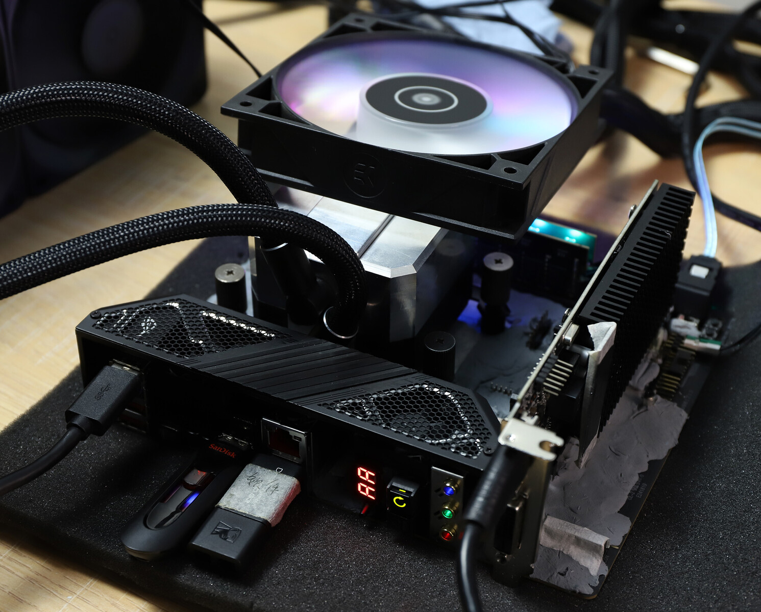
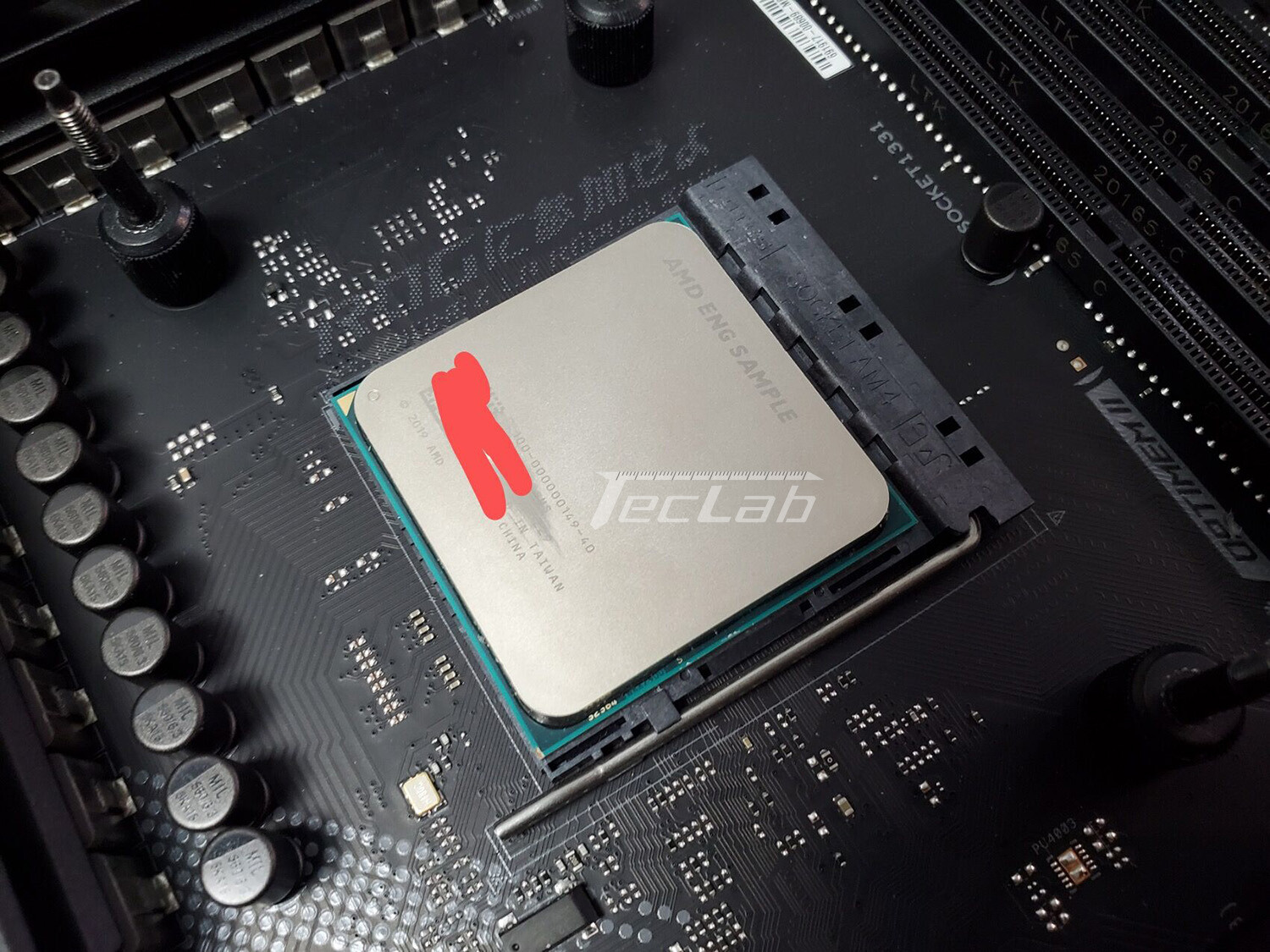
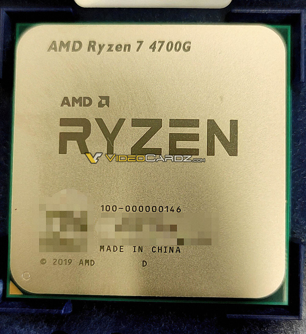
AMD is planning to immediately update its product stack to counter the Intel 10th gen Core "Comet Lake-S" desktop processor family. Codenamed "Matisse Refresh," the processor will use existing IP, based on the 7 nm "Zen 2" microarchitecture, but could improve in areas such as clock-speeds. As it now stands, the Ryzen 9 3900X appears unfazed by the i9-10900K and i7-10700K at its new $410 price, however, competitiveness of the 3800X and 3700X could buckle under pressure from the i7-10700 series (K, KF, non-K, and F), as well as the Core i5-10600 series. To this effect, we're hearing rumors of a "Ryzen 7 3750X" and "Ryzen 7 3850X" seeing the light of the day soon, with an early-June announcement, and early-July market availability. References to the 3750X date back to October 2019.

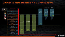
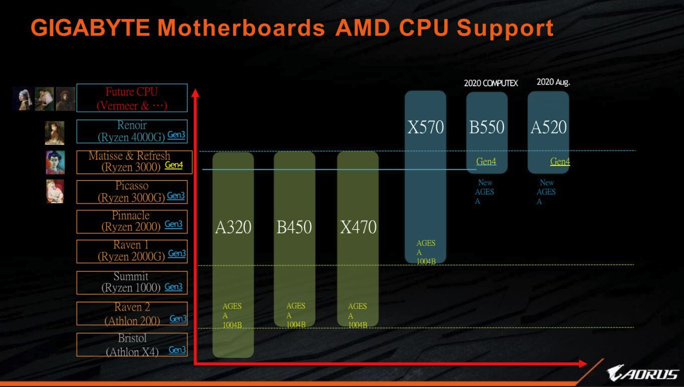
Rumors of "Matisse Refresh" gained traction when WCCFTech editor Hassan Mujtaba tweeted a slide from a GIGABYTE AMD B550 motherboard series pre-launch presentation, which references GIGABYTE's own interpretation of AMD's roadmap. It lists out every CPU microarchitecture for the AM4 platform, and right next to "Matisse" is "& Refresh," confirming that "Matisse Refresh" is real. A microarchitecture "refresh" needn't even involve any physical changes to the processor design, core-counts, or architecture, and can sometimes even indicate something as simple as a second major wave of SKUs that replace existing SKUs in the market, leading to their phase-out (eg: Intel "Haswell Refresh" retaining the 4th gen Core model numbering). The slide also adds weight to the theory that desktop "Renoir," like its mobile counterpart, lacks PCIe gen 4.0. The slide also talks about AMD introducing the entry-level A520 desktop chipset in August, which will support PCIe gen 4 when paired with a capable processor.

Samsung Expands its Foundry Capacity with A New Production Line in Pyeongtaek

Samsung Electronics Co., Ltd., a world leader in advanced semiconductor technology, today announced plans to boost its foundry capacity at the company's new production line in Pyeongtaek, Korea, to meet growing global demand for cutting-edge extreme ultraviolet (EUV) solutions.

The new foundry line, which will focus on EUV-based 5 nanometer (nm) and below process technology, has just commenced construction this month and is expected to be in full operation in the second half of 2021. It will play a pivotal role as Samsung aims to expand the use of state-of-the-art process technologies across a myriad of current and next generation applications, including 5G, high-performance computing (HPC) and artificial intelligence (AI).

SMIC Begins Mass-Production of 14nm FinFET SoCs for Huawei HiSilicon

Semiconductor Manufacturing International Corporation (SMIC), the state-backed Mainland Chinese semiconductor foundry, announced that it commenced mass-production of 14 nm FinFET SoCs for Huawei's HiSilicon subsidiary, a mere one month since Huawei shifting chip orders from TSMC to it. The company is manufacturing Kirin 710A is a revision of the original Kirin 710 SoC from 2018, built on SMIC's 14 nm node. The 4G-era SoC is capable of powering mid-range smartphones for Huawei's Honor brand, and uses an Arm big.LITTLE setup of Cortex A53 and Cortex A57 cores. This represents a major milestone not just for SMIC, but also Huawei, which has seen the company's isolation from cutting-edge overseas fabs such as TSMC. Much of Huawei's fate is riding on the success of SMIC's next-generation N+1 node, which purportedly offers a 57 percent energy-efficiency gain over 14 nm FinFET, rivaling sub-10 nm nodes such as 7 nm; enabling Huawei to build 5G-era SoCs.

AMD Ryzen 7 4700G "Renoir" Desktop Processor Pictured

Here is the first picture of the AMD Ryzen 7 4700G, the company's upcoming socket AM4 APU based on the 7 nm "Renoir" silicon, courtesy of VideoCardz. The picture reveals a standard-looking socket AM4 chip with commercial name and OPN markings (100-000000146), matching the Igor's Lab OPN code leak from earlier this week. The Ryzen 7 4700G offers an 8-core/16-thread CPU based on the "Zen 2" microarchitecture, and an integrated graphics solution that combines the SIMD machinery of the "Vega" graphics architecture, with the updated display- and media engines of "Navi." The iGPU is configured with 8 CUs (512 stream processors), which on the 4700G has an impressive maximum engine boost clock of 2.10 GHz, according to the Igor's Lab story.

The 8-core/16-thread CPU of the Ryzen 7 4700G has a nominal clock speed of 3.60 GHz, and a maximum boost frequency of 4.45 GHz, with several Precision Boost power-states in both directions of the nominal clock. The CPU features 512 KB of L2 cache per core, and 8 MB of shared L3 cache (4 MB per CCX). The iGPU engine clock goes all the way up to 2.10 GHz, which could help it overcome some of the CU deficit vs. "Picasso," which has 11 CUs (704 stream processors), but clocked only up to 1.40 GHz. Since the Ryzen 5 3400G has an unlocked multiplier, it stands to reason that even the 4700G could. If the platform I/O of "Renoir" in its mobile avatar is anything to go by, then the 4700G could feature a limited PCI-Express x8 lane setup for its PEG port. AMD is rating the TDP of the 4700G at 65 W.

NVIDIA Ampere A100 Has 54 Billion Transistors, World's Largest 7nm Chip

Not long ago, Intel's Raja Koduri claimed that the Xe HP "Ponte Vecchio" silicon was the "big daddy" of Xe GPUs, and the "largest chip co-developed in India," larger than the 35 billion-transistor Xilinix VU19P FPGA co-developed in the country. It turns out that NVIDIA is in the mood for setting records. The "Ampere" A100 silicon has 54 billion transistors crammed into a single 7 nm die (not counting transistor counts of the HBM2E memory stacks).

NVIDIA claims a 20 Times boost in both AI inference and single-precision (FP32) performance over its "Volta" based predecessor, the Tesla V100. The chip also offers a 2.5X gain in FP64 performance over "Volta." NVIDIA has also invented a new number format for AI compute, called TF32 (tensor float 32). TF32 uses 10-bit mantissa of FP16, and the 8-bit exponent of FP32, resulting in a new, efficient format. NVIDIA attributes its 20x performance gains over "Volta" to this. The 3rd generation tensor core introduced with Ampere supports FP64 natively. Another key design focus for NVIDIA is to leverage the "sparsity" phenomenon in neural nets, to reduce their size, and improve performance.

Fujitsu Completes Delivery of Fugaku Supercomputer

Fujitsu has today officially completed the delivery of the Fugaku supercomputer to the Riken scientific research institute of Japan. This is a big accomplishment as the current COVID-19 pandemic has delayed many happenings in the industry. However, Fujitsu managed to play around that and deliver the supercomputer on time. The last of 400 racks needed for the Fugaku supercomputer was delivered today, on May 13th, as it was originally planned. The supercomputer is supposed to be fully operational starting on the physical year of 2021, where the installation and setup will be done before.

As a reminder, the Fugaku is an Arm-based supercomputer consisting out of 150 thousand A64FX CPUs. These CPUs are custom made processors by Fujitsu based on Arm v8.2 ISA, and they feature 48 cores built on TSMC 7 nm node and running above 2 GHz. Packing 8.786 billion transistors, this monster chips use HBM2 memory instead of a regular DDR memory interface. Recently, a prototype of the Fugaku supercomputer was submitted to the Top500 supercomputer list and it came on top for being the most energy-efficient of all, meaning that it will be as energy efficient as it will be fast. Speculations are that it will have around 400 PetaFlops of general compute power for Dual-Precision workloads, however, for the specific artificial intelligence applications, it should achieve ExaFLOP performance target.
K SuperComputer

AMD Ryzen 7 4700G is "Renoir" Desktop AM4 Processor: 8-core/16-thread with "Vega" iGPU

It was only a matter of time before AMD brought its 7 nm "Renoir" APU silicon onto the desktop platform. The first such chip just hit the radar as the Ryzen 7 4700G. This would be the first desktop Ryzen APU graded as Ryzen 7, thanks to its CPU core count. The 4700G features an 8-core/16-thread CPU based on the "Zen 2" microarchitecture. The iGPU is a hybrid between "Vega" and "Navi."

The "Renoir" iGPU features the SIMD components of "Vega," but with the display- and multimedia-engines of "Navi." The iGPU apparently maxes out on 8 NGCUs on "Renoir," amounting to 512 stream processors. Increased iGPU engine clocks attempt to make up the CU deficit compared to the previous-generation "Picasso" (8 vs. 11). The CPU features 512 KB of L2 cache per core, and 8 MB of shared L3 cache (4 MB per CCX). An AoTS run in which the processor is paired with a Radeon RX 5700 XT graphics card surfaced on social media. Bringing "Renoir" to the desktop platform at prices competitive with Intel's 10th generation Core i3 thru Core i7 will be critical for AMD, as it nullifies a key advantage Intel has - integrated graphics, so the processors could make it to the vast majority of non-gaming builds with high CPU performance demand.

Update May 10th: A possible UserBenchmark submission of this processor, where it carries the engineering sample number "100-000000149-40_40/30_Y" surfaced. It's shown having clock speeds of 3.00 GHz base and 4.00 GHz boost. We know this is a desktop platform looking at its ASRock B550 Taichi motherboard and Micron-supplied standard DIMM.

AMD Announces Ryzen PRO 4000 Series Mobile Processors

Today, AMD announced global availability of the world's first x86 7 nm commercial notebook processors, the AMD Ryzen PRO 4000 Series Mobile family, delivering the most cores and threads in an ultrathin business notebook. These new processors are fully optimized for remote work capabilities and designed to take business computing to the next level with multi-threading performance for modern productivity. Robust enterprise designs from HP and Lenovo powered by AMD Ryzen PRO 4000 Series Mobile Processors are expected to be available worldwide starting in the first half of 2020, with anywhere-anytime productivity, multiple layers of security features, seamless manageability and reliable longevity.

"With the launch of AMD Ryzen PRO 4000 Series Mobile Processors, AMD once again defines the new standard for PC experiences - from high-end desktop computing to ultrathin and gaming notebooks, and now the modern business notebook," said Saeid Moshkelani, senior vice president and general manager, client business unit, AMD. "Built on the ground-breaking "Zen 2" architecture and 7 nm process technology, the AMD Ryzen for Business portfolio delivers advanced performance, reliable security features, impressive battery life and advanced manageability to significantly elevate the capabilities of the ultrathin notebook in any work environment."

NVIDIA Underestimated AMD's Efficiency Gains from Tapping into TSMC 7nm: Report

A DigiTimes premium report, interpreted by Chiakokhua, aka Retired Engineer, chronicling NVIDIA's move to contract TSMC for 7 nm and 5 nm EUV nodes for GPU manufacturing, made a startling revelation about NVIDIA's recent foundry diversification moves. Back in July 2019, a leading Korean publication confirmed NVIDIA's decision to contract Samsung for its next-generation GPU manufacturing. This was a week before AMD announced its first new-generation 7 nm products built for the TSMC N7 node, "Navi" and "Zen 2." The DigiTimes report reveals that NVIDIA underestimated the efficiency gains AMD would yield from TSMC N7.

With NVIDIA's bonhomie with Samsung underway, and Apple transitioning to TSMC N5, AMD moved in to quickly grab 7 nm-class foundry allocation and gained prominence with the Taiwanese foundry. The report also calls out a possible strategic error on NVIDIA's part. Upon realizing the efficiency gains AMD managed, NVIDIA decided to bet on TSMC again (apparently without withdrawing from its partnership with Samsung), only to find that AMD had secured a big chunk of its nodal allocation needed to support its growth in the x86 processor and discrete GPU markets. NVIDIA has hence decided to leapfrog AMD by adapting its next-generation graphics architectures to TSMC's EUV nodes, namely the N7+ and N5. The report also speaks of NVIDIA using its Samsung foundry allocation as a bargaining chip in price negotiations with TSMC, but with limited success as TSMC established its 7 nm-class industry leadership. As it stands now, NVIDIA may manufacture its 7 nm-class and 5 nm-class GPUs on both TSMC and Samsung.

TSMC Secures Orders from NVIDIA for 7nm and 5nm Chips

TSMC has reportedly secured orders from NVIDIA for chips based on its 7 nm and 5 nm silicon fabrication nodes, sources tell DigiTimes. If true, it could confirm rumors of NVIDIA splitting its next-generation GPU manufacturing between TSMC and Samsung. The Korean semiconductor giant is commencing 5 nm EUV mass production within Q2-2020, and NVIDIA is expected to be one of its customers. NVIDIA is expected to shed light on its next-gen graphics architecture at the GTC 2020 online event held later this month. With its "Turing" architecture approaching six quarters of market presence, it's likely that the decks are being cleared for a new architecture not just in HPC/AI compute product segment, but also GeForce and Quadro consumer graphics cards. Splitting manufacturing between TSMC and Samsung would help NVIDIA disperse any yield issue arriving from either foundry's EUV node, and give it greater bargaining power with both.

Tachyum Prodigy is a Small 128-core Processor with Crazy I/O Options, 64-core Sibling Enroute Production

Silicon Valley startup Tachyum, founded in 2016, is ready with its crowning product, the Tachyum Prodigy. The startup recently received an investment from the Slovak government in hopes of job-creation in the country. The Prodigy is what its makers call "a universal processor," which "outperforms the fastest Xeon at 10X lower power." The company won't mention what machine architecture it uses (whether it's Arm or MIPS, or its own architecture). Its data-sheet is otherwise full of specs that scream at you.

To begin with, its top trim, the Prodigy T16128, packs 128 cores on a single package, complete with 64-bit address space, 512-bit vector extensions, matrix multiplication fixed-function hardware that accelerate AI/ML, and 4 IPC at up to 4.00 GHz core clock. Tachyum began the processor's software-side support, with an FPGA emulator in December 2019 (so you can emulate the processor on an FPGA and begin developing for it), C/C++ and Fortran compilers; debuggers and profilers, tensorflow compilers, and a Linux distribution that's optimized it. The I/O capabilities of this chip are something else.

AMD Confirms Zen 3 and RDNA2 by Late-2020

AMD in its post Q1-2020 earnings release disclosures stated that the company is "on track" to launching its next-generation "Zen 3" CPU microarchitecture and RDNA2 graphics architecture in late-2020. The company did not reveal in what shape or form the two will debut. AMD is readying "Zen 3" based EPYC "Milan" enterprise processors, "Vermeer" Ryzen desktop processors, and "Cezanne" Ryzen mobile APUs based on "Zen 3," although there's no word on which product line the microarchitecture will debut with. "Zen 3" compute dies (CCDs) are expected to do away with the quad-core compute complex (CCX) arrangement of cores, and are expected to be built on a refined 7 nm-class silicon fabrication process, either TSMC N7P or N7+.

The only confirmed RDNA2 based products we have as of now are the semi-custom SoCs that drive the Sony PlayStation 5 and Microsoft Xbox Series X next-generation consoles, which are expected to debut by late-2020. The AMD tweet, however, specifies "GPUs" (possibly referring to discrete GPUs). Also, with AMD forking its graphics IP to RDNA (for graphics processors) and CDNA (for headless compute accelerators), we're fairly sure AMD is referring to a Radeon RX or Radeon Pro launch in the tweet. Microsoft's announcement of the DirectX 12 Ultimate logo is expected to expedite launch of Radeon RX discrete GPUs based on RDNA2, as the current RDNA architecture doesn't meet the logo requirements.

Intel's First 7nm Client Microarchitecture is "Meteor Lake"

Intel's first client-segment processor microarchitecture built on its own 7 nm silicon fabrication process will be codenamed "Meteor Lake." The codename began surfacing in driver files and technical documents, one of which was screengrabbed and leaked to the web by Komachi Ensaka. Not much else is known about it, except that it succeeds the 10 nm++ "Alder Lake," an ambitious attempt by Intel to replicate Arm big.LITTLE heterogenous core technology on the x86 architecture, by combining a number of high-power cores with high-efficiency cores on a single piece of silicon. Intel "Lakefield," headed toward mass-production within this year, is the first such heterogenous core.

Older reports throughout 2019-20 speculate "Meteor Lake" (known at the time only by its name), could come out at a time when Intel monetizes its "Golden Cove" high-performance CPU core. It's quite likely that like "Alder Lake," it could be a heterogenous chip targeting several client form-factors, mobile and desktop. The company could leverage its 7 nm process - claimed to rival TSMC 5 nm-class in transistor density - in turning up core-counts over "Alder Lake." We'll learn more about "Meteor Lake" as we crawl toward its 2022 launch window, if it still holds up.

DigiTimes: TSMC Kicking Off Development of 2nm Process Node

A report via DigiTimes places TSMC as having announced to its investors that exploratory studies and R&D for the development of the 2 nm process node have commenced. As today's leading semiconductor fabrication company, TSMC doesn't seem to be one resting on its laurels. Their 7 nm process and derivatives have already achieved a 30% weight on the company's semiconductor orders, and their 5 nm node (which will include EUV litography) is set to hit HVM (High Volume Manufacturing) in Q2 of this year. Apart from that, not much more is known on 2 nm.

After 5 nm, which is expected to boats of an 84-87% transistor density gain over the current 7nm node, the plans are to go 3nm, with TSMC expecting that node to hit mass production come 2022. Interestingly, TSMC is planning to still use FinFET technology for its 3 nm manufacturing node, though in a new GAAFET (gate-all-around field-effect transistor) technology. TSMC's plans to deploy FinFET in under 5nm manufacturing is something that many industry analysts and specialist thought extremely difficult to achieve, with expectations for these sub-5nm nodes to require more exotic materials and transistor designs than TSMC's apparent plans
Return to Keyword Browsing
May 21st, 2024 05:14 EDT change timezone

New Forum Posts

Popular Reviews

Controversial News Posts