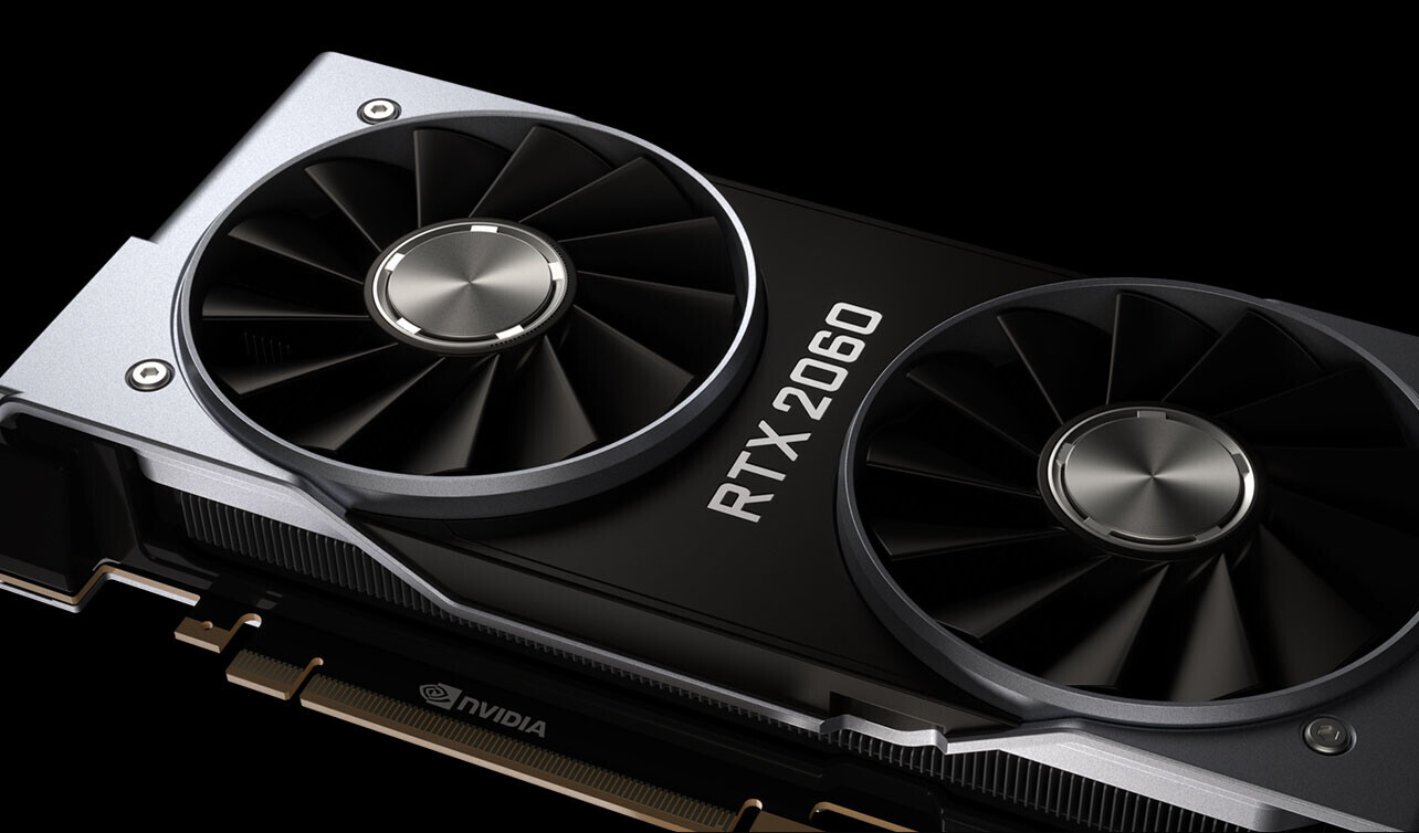
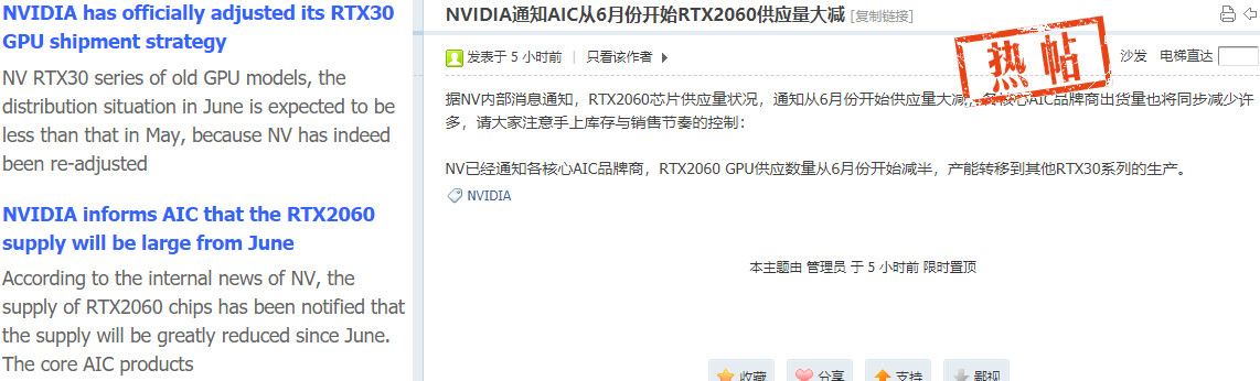
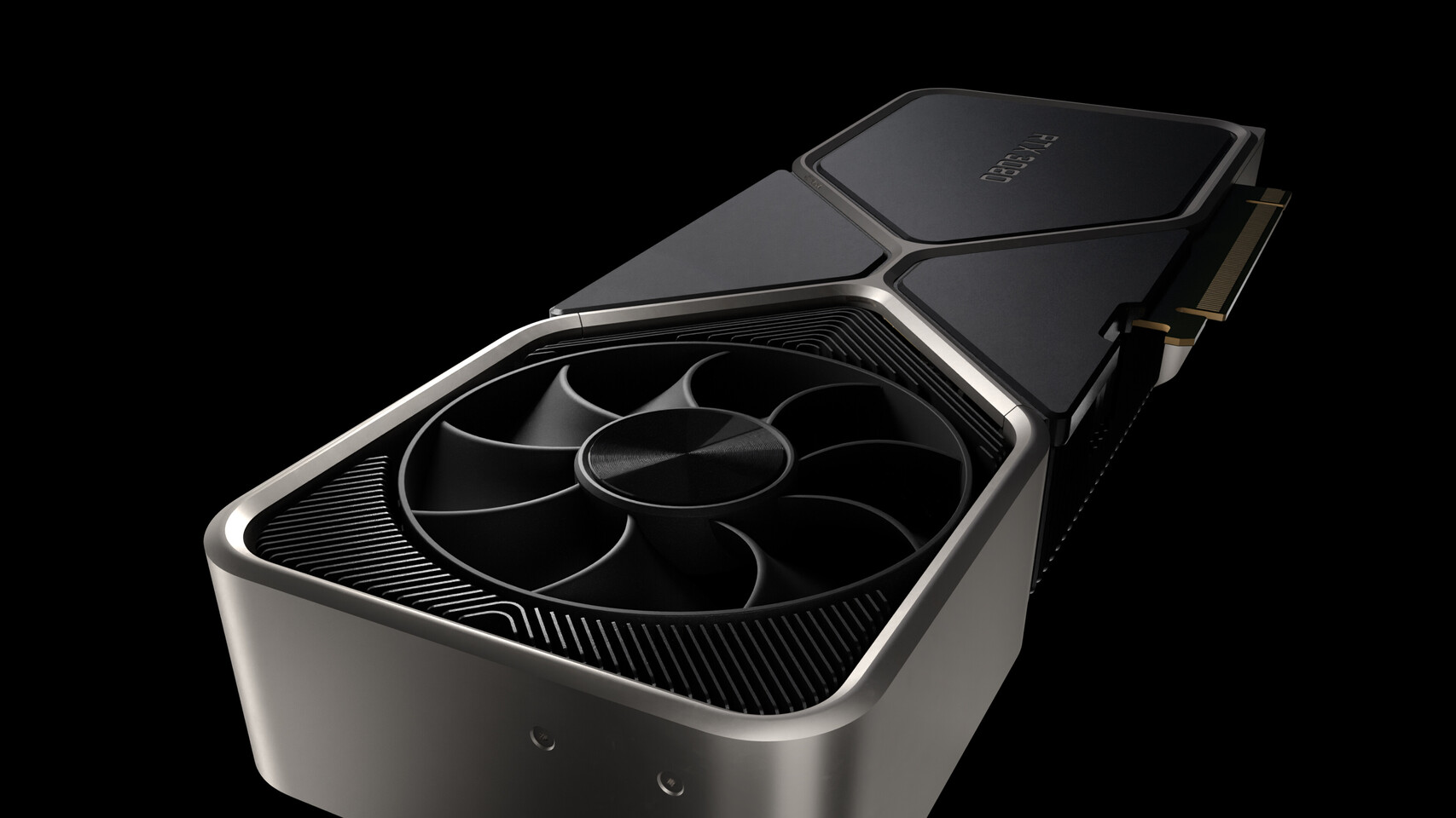
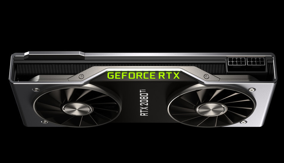
NVIDIA Reportedly Cutting RTX 2060 Fabrication to Focus on RTX 30-series
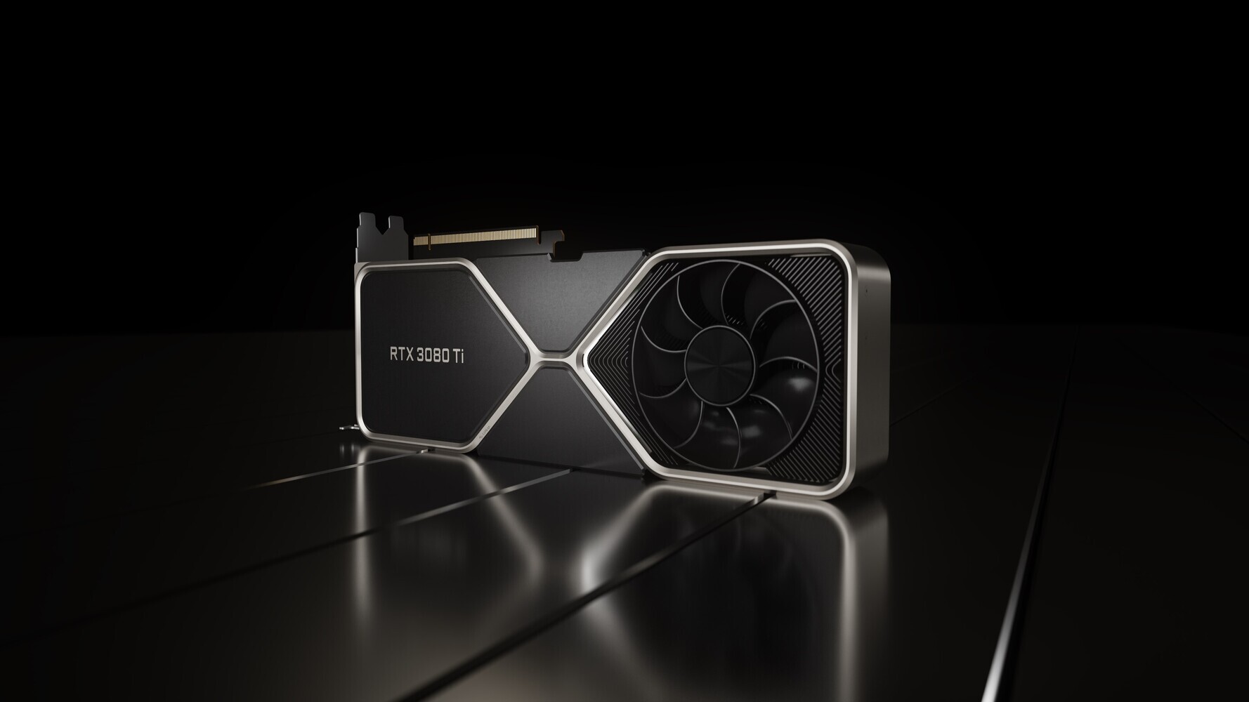
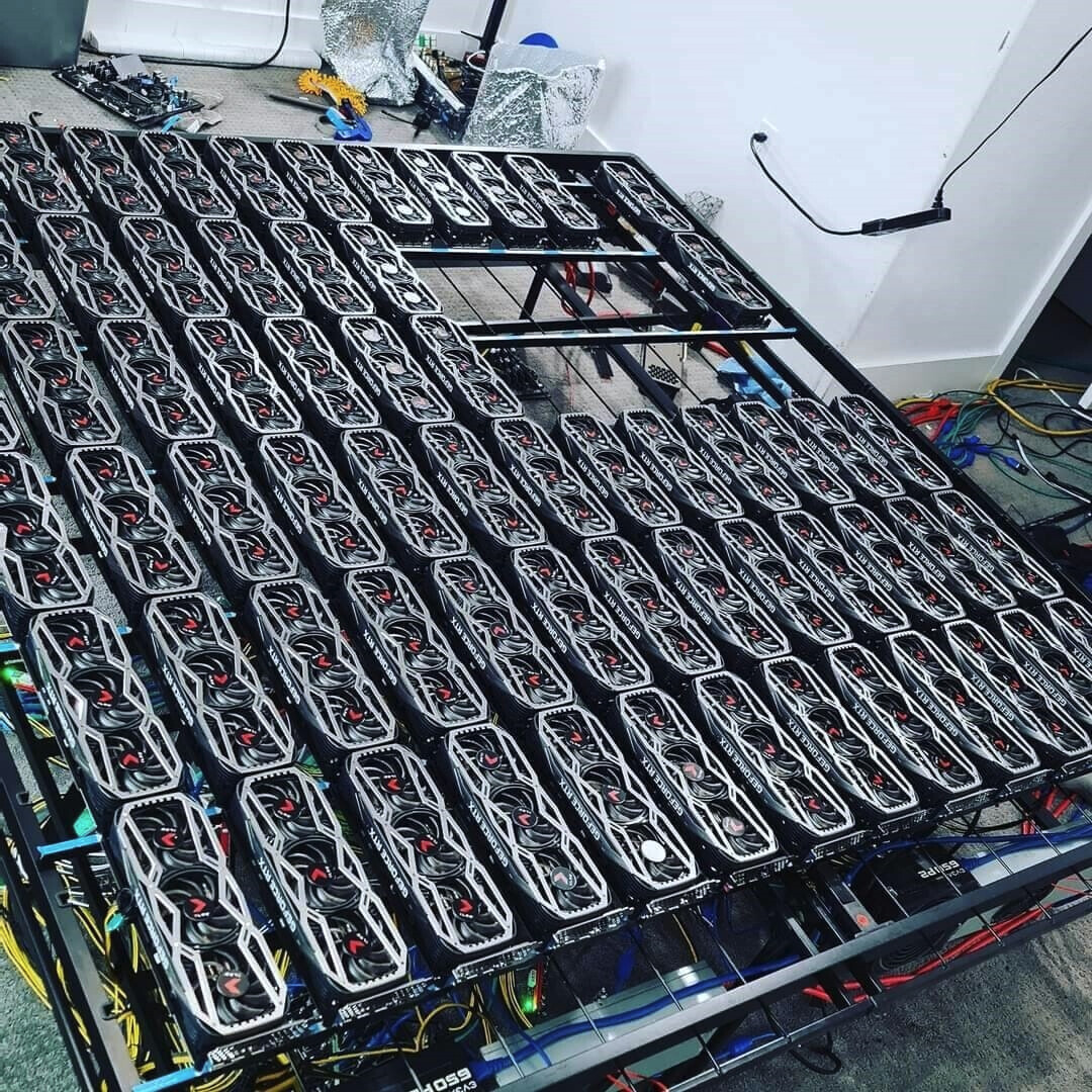
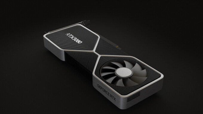
NVIDIA is reported to be cutting down on production of its highly popular RTX 2060 graphics card, in a bid to increase production of the RTX 30-series graphics cards that still elude most consumers looking to get one on their gaming rig. The decision may be motivated by increased margins on RTX 30-series products, as well as by the continuing component shortage in the industry, with even GDDR6 becoming a limiting factor to production capability.
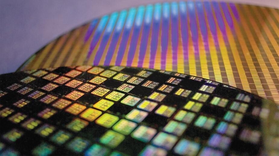
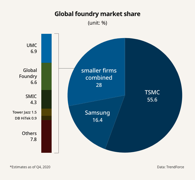
While one might consider this a strange move at face value (Turing is manufactured on TSMC's 12 nm node, whilst Ampere is manufactured on Samsung's 8 nm), the fact of the matter is that there are a multitude of components required for GPUs besides the graphics processing silicon proper; and NVIDIA essentially sells ready-to-produce kits to AICs (Add-in-Card Partners) which already include all the required components, circuitry, and GPU slice to put together. And since supply on most components and even simple logic is currently strained, every component in an RTX 2060-allocated kit could be eating into final production capacity for the RTX 30-series graphics cards - hence the decision to curb the attempt to satiate pent-up demand with a last-generation graphics card and instead focusing on current-gen hardware.


While one might consider this a strange move at face value (Turing is manufactured on TSMC's 12 nm node, whilst Ampere is manufactured on Samsung's 8 nm), the fact of the matter is that there are a multitude of components required for GPUs besides the graphics processing silicon proper; and NVIDIA essentially sells ready-to-produce kits to AICs (Add-in-Card Partners) which already include all the required components, circuitry, and GPU slice to put together. And since supply on most components and even simple logic is currently strained, every component in an RTX 2060-allocated kit could be eating into final production capacity for the RTX 30-series graphics cards - hence the decision to curb the attempt to satiate pent-up demand with a last-generation graphics card and instead focusing on current-gen hardware.