News Posts matching #Ampere

Return to Keyword Browsing

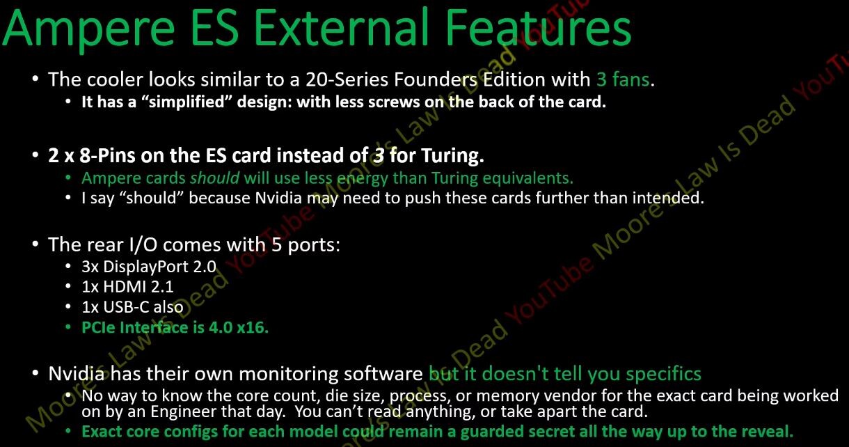
NVIDIA Ampere Cooling Solution Heatsink Pictured, Rumors of Airflow Magic Quashed

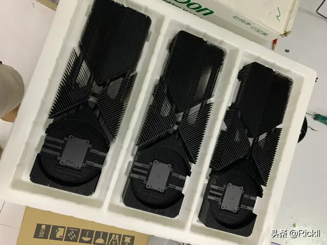
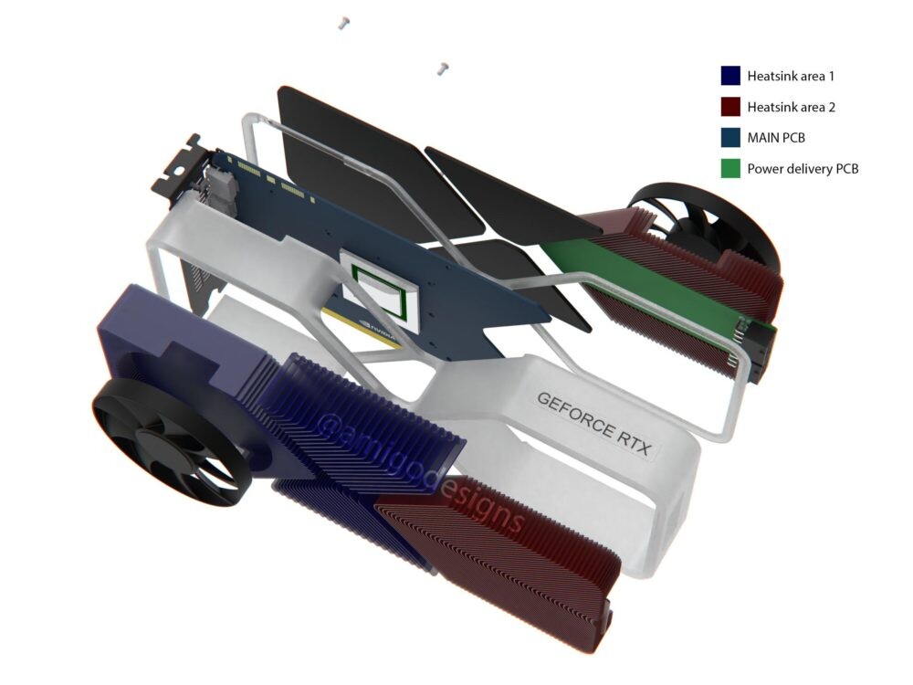
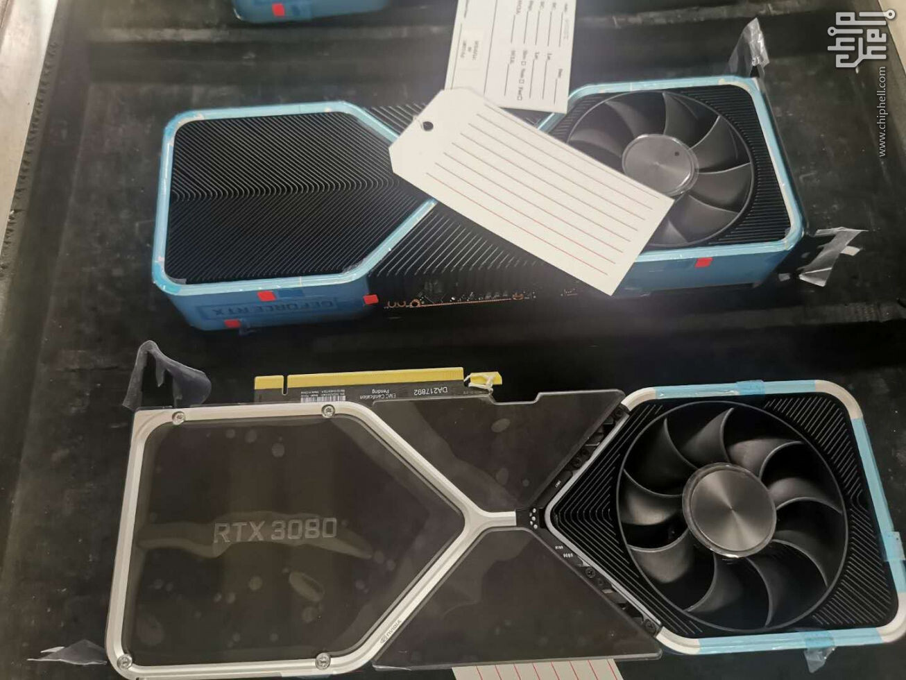
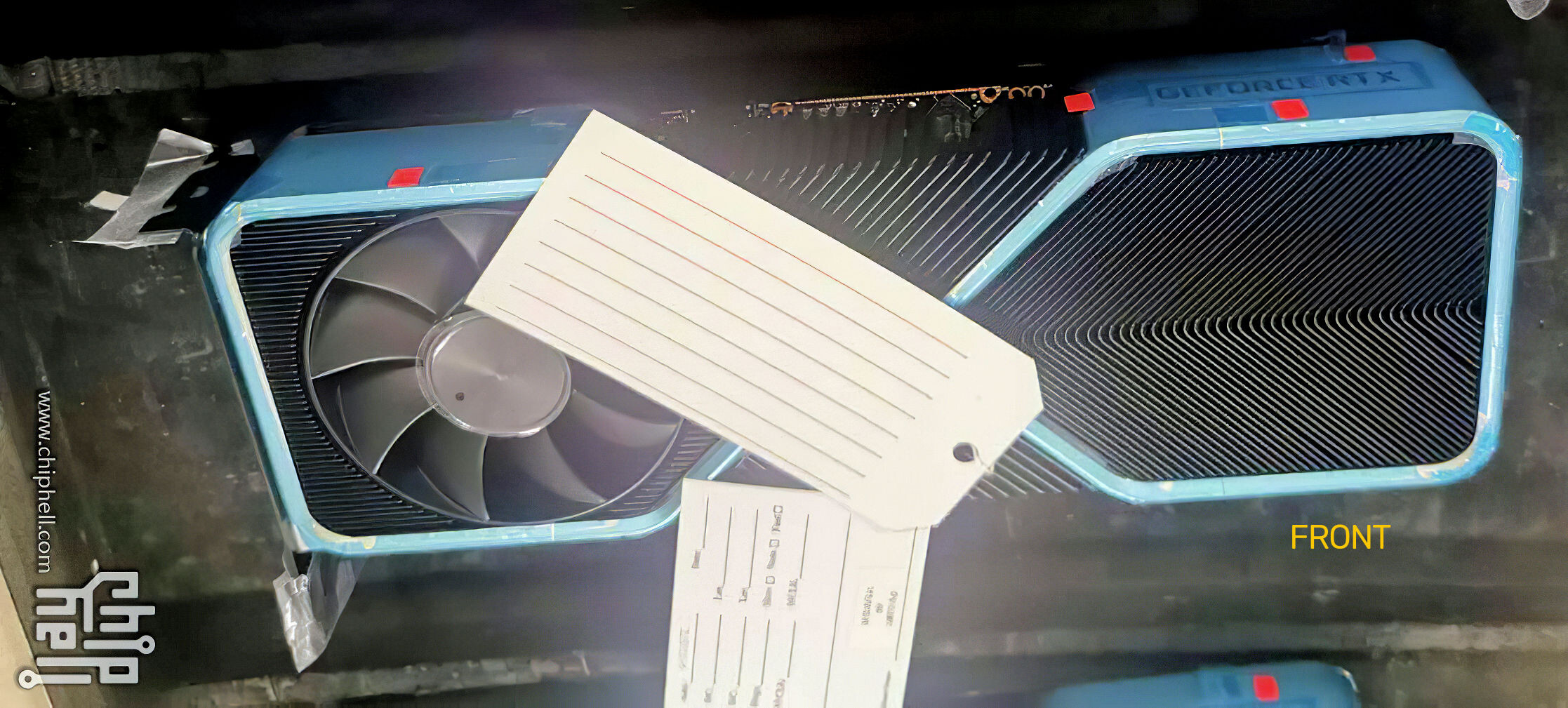
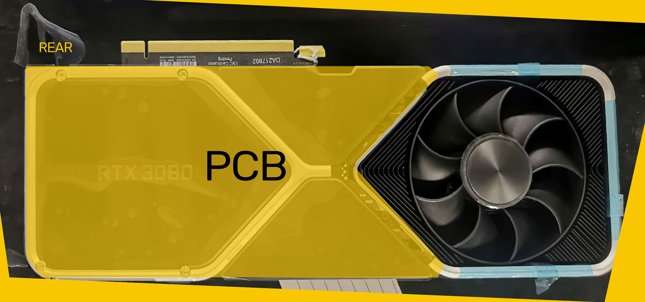
Although still a blurry-cam pic, this new picture of three GeForce RTX 3080 "Ampere" graphics card reference heatsinks on a factory-floor reveals exactly how the cooling solution works. The main heat-dissipation component appears to be a vapor chamber base, above which there are four flattened copper heat pipes, which hold the cooler's four aluminium fin arrays together. The first array is directly above the CPU/memory/VRM area, and consists of a dense stack of aluminium fins that make up a cavity for the fan on the obverse side of the graphics card. This fan vents air onto the first heatsink element, and some of its air is guided by the heatsink to two trapezium shaped aluminium fin-stacks that pull heat from the flattened heat pipes, and get airflow from the obverse fan.

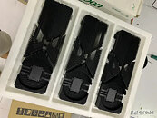
The heat pipes make their way to the card's second dense aluminium fin-stack. This fin-stack is as thick as the card itself, as there's no PCB here. This fin-stack is ventilated by the card's second fan, located on the reverse side, which pulls air through this fin-stack and vents upward. We attempted to detail the cooling solution, the card, and other SKU details in an older article. We've also added a picture of a Sapphire Radeon RX Vega 56 Pulse graphics card. This NVIDIA heatsink is essentially like that, but with the second fan on the other side of the card to make it look more complicated than it actually is.

NVIDIA's Next-Gen Reference Cooler Costs $150 By Itself, to Feature in Three SKUs

Pictures of alleged next-generation GeForce "Ampere" graphics cards emerged over the weekend, which many of our readers found hard to believe. It's features a dual-fan cooling solution, in which one of the two fans is on the reverse side of the card, blowing air outward from the cooling solution, while the PCB extends two-thirds the length of the card. Since then, there have been several fan-made 3D renders of the card. NVIDIA is not happy with the leak, and started an investigation into two of its contractors responsible for manufacturing Founders Edition (reference design) GeForce graphics cards, Foxconn and BYD (Build Your Dreams), according to a report by Igor's Lab.

According to the report, the cooling solution, which looks a lot more overengineered than the company's RTX 20-series Founders Edition cooler, costs a hefty USD $150, or roughly the price of a 280 mm AIO CLC. It wouldn't surprise us if Asetek's RadCard costs less. The cooler consists of several interconnected heatsink elements with the PCB in the middle. Igor's Lab reports that the card is estimated to be 21.9 cm in length. Given its cost, NVIDIA is reserving this cooler for only the top three SKUs in the lineup, the TITAN RTX successor, the RTX 2080 Ti successor, and the RTX 2080/SUPER successor.

NVIDIA GeForce RTX 3080 Pictured?

Here are what could be the very first pictures of a reference NVIDIA GeForce RTX 3080 "Ampere" graphics card revealing an unusual board design, which is the biggest departure in NVIDIA's design schemes since the original GeForce TITAN. It features a dual-fan aluminium fin-stack cooler, except that one of its fans is located on the obverse side, and the other on the reverse side of the card. The PCB of the card appears to extend only two-thirds the length of the card, ending in an inward cutout, beyond which there's only an extension of the cooling solution. The cooler shroud, rather than being a solid covering of the heatsink, is made of aluminium heatsink ridges. All in all, a very unusual design, which NVIDIA could implement on its top-tier SKUs, such as the RTX 3080, RTX 3080 Ti, and in a cosmetic form on lower SKUs. We get the feeling that "Cyberpunk 2077" has influenced this design.

Microsoft Builds a Supercomputer for AI

Microsoft has held a Build 2020 conference for developers from all over the world, and they live-streamed it online. Among some of the announcements, Microsoft has announced a new supercomputer dedicated to the OpenAI company, which works on building Artificial General Intelligence (AGI). The new supercomputer is a part of Microsoft's Azure cloud infrastructure and it will allow OpenAI developers to train very large scale machine learning models in the cloud. The supercomputer is said to be the fifth most powerful supercomputer in the world with specifications of "more than 285,000 CPU cores, 10,000 GPUs and 400 gigabits per second of network connectivity for each GPU server."

Specific information wasn't announced and we don't know what CPUs and GPUs go into this machine, but we can speculate that the latest Nvidia A100 "Ampere" GPU could be used. The company hasn't yet submitted its entry to the Top500 website, so we can't keep track of the FLOPs count and see what power it holds.
Microsoft Azure Data Center

NVIDIA Discontinues the Tesla Brand to Avoid Confusion with Tesla Car Maker

At its ambitious "Ampere" A100 Tensor Core processor reveal, the "Tesla" brand was nowhere to be seen. Heise.de reports that the company has decided to discontinue "Tesla" as the top-level brand for its HPC, AI, and scalar compute accelerator product line. NVIDIA introduced the Tesla compute accelerator brand along with its "Tesla" graphics architecture. It was the first major GPGPU product, and saw CUDA take flight as a prominent scalar compute language.

Over the years, NVIDIA kept the Tesla moniker as a top-level brand (alongside GeForce and Quadro), with an alphabetic portion of the model numbers denoting the graphics architecture the accelerator is based on (eg: Tesla P100 being "Pascal" based, K10 being "Kepler" based, and M40 being "Maxwell" based). The Tesla T4, based on "Turing," is the final product with the old nomenclature. Interestingly, Heise reports that NVIDIA dropped the name to avoid confusion with fellow Californian brand Tesla Inc.

Atos Launches First Supercomputer Equipped with NVIDIA A100 Tensor Core GPU

Atos, a global leader in digital transformation, today announces its new BullSequana X2415, the first supercomputer in Europe to integrate NVIDIA's Ampere next-generation graphics processing unit architecture, the NVIDIA A100 Tensor Core GPU. This new supercomputer blade will deliver unprecedented computing power to boost application performance for HPC and AI workloads, tackling the challenges of the exascale era. The BullSequana X2415 blade will increase computing power by more than 2x and optimize energy consumption thanks to Atos' 100% highly efficient water-cooled patented DLC (Direct Liquid Cooling) solution, which uses warm water to cool the machine.

Forschungszentrum Jülich will integrate this new blade into its booster module, extending its existing JUWELS BullSequana supercomputer, making it the first system worldwide the use this new technology. The JUWELS Booster will provide researchers across Europe with significantly increased computational resources. Some of the projects it will fuel are the European Commission's Human Brain Project and the Jülich Laboratories of "Climate Science" and "Molecular Systems". Once fully deployed this summer the upgraded supercomputing system, operated under ParTec's software ParaStation Modulo, is expected to provide a computational peak performance of more than 70 Petaflops/s making it the most powerful supercomputer in Europe and a showcase for European exascale architecture.

NVIDIA "Ampere" Designed for both HPC and GeForce/Quadro

NVIDIA CEO Jensen Huang in a pre-GTC press briefing stressed that the upcoming "Ampere" graphics architecture will spread across both the company's compute-accelerator and commercial graphics product lines. The architecture makes its debut later today with the Tesla A100 HPC processor for breakthrough AI acceleration. It's unlikely that any GeForce products will be formally announced this month, with rumors pointing to a GeForce "Ampere" product launch at a gaming-focused event in September, close to "Cyberpunk 2077" launch.

It was earlier believed that NVIDIA had forked its breadwinning IP into two lines, one focused on headless scalar compute, and the other on graphics products through the company's GeForce and Quadro product lines. To that effect, its "Volta" architecture focused on scalar-compute (with the exception of the forgotten TITAN V); and the "Turing" architecture focused solely on GeForce and Quadro. It was then believed that "Ampere" will focus on compute, and the so-called "Hopper" would be this generation's graphics-focused architecture. We now know that won't be the case. We've compiled a selection of GeForce Ampere rumors in this article.

NVIDIA Tesla A100 "Ampere" AIC (add-in card) Form-Factor Board Pictured

Here's the first picture of a Tesla A100 "Ampere" AIC (add-in card) form-factor board, hot on the heals of the morning big A100 reveal. The AIC card is a bare PCB, which workstation builders will add compatible cooling solutions on. The PCB features the gigantic GA100 processor with its six HBM2E stacks, in the center, surrounded by VRM components, and I/O on three sides. On the bottom side, you will find a conventional PCI-Express 4.0 x16 host interface. Above it, are NVLink fingers. The rear I/O has high-bandwidth network interfaces (likely 200 Gbps InfiniBand), by Mellanox. The tail end has hard points for 12 V power input. Find juicy details of the GA100 in our older article.

NVIDIA Ampere A100 Has 54 Billion Transistors, World's Largest 7nm Chip

Not long ago, Intel's Raja Koduri claimed that the Xe HP "Ponte Vecchio" silicon was the "big daddy" of Xe GPUs, and the "largest chip co-developed in India," larger than the 35 billion-transistor Xilinix VU19P FPGA co-developed in the country. It turns out that NVIDIA is in the mood for setting records. The "Ampere" A100 silicon has 54 billion transistors crammed into a single 7 nm die (not counting transistor counts of the HBM2E memory stacks).

NVIDIA claims a 20 Times boost in both AI inference and single-precision (FP32) performance over its "Volta" based predecessor, the Tesla V100. The chip also offers a 2.5X gain in FP64 performance over "Volta." NVIDIA has also invented a new number format for AI compute, called TF32 (tensor float 32). TF32 uses 10-bit mantissa of FP16, and the 8-bit exponent of FP32, resulting in a new, efficient format. NVIDIA attributes its 20x performance gains over "Volta" to this. The 3rd generation tensor core introduced with Ampere supports FP64 natively. Another key design focus for NVIDIA is to leverage the "sparsity" phenomenon in neural nets, to reduce their size, and improve performance.

NVIDIA Tesla A100 GPU Pictured

Thanks to the sources of VideoCardz, we now have the first picture of the next-generation NVIDIA Tesla A100 graphics card. Designed for computing oriented applications, the Tesla A100 is a socketed GPU designed for NVIDIA's proprietary SXM socket. In a post few days ago, we were suspecting that you might be able to fit the Tesla A100 GPU in the socket of the previous Volta V100 GPUs as it is a similar SXM socket. However, the mounting holes have been re-arranged and this one requires a new socket/motherboard. The Tesla A100 GPU is based on GA100 GPU die, which we don't know specifications of. From the picture, we can only see that there is one very big die attached to six HBM modules, most likely HBM2E. Besides that everything else is unknown. More details are expected to be announced today at the GTC 2020 digital keynote.
NVIDIA Tesla A100

NVIDIA CEO Jensen Huang has been Cooking the World's Largest GPU - Is this Ampere?

NVIDIA is rumored to introduce their next-generation Ampere architecture very soon, at its GTC event happening on May 14th. We're expecting to see an announcement for the successor to the company's DGX lineup of pre-built compute systems—using the upcoming Ampere architecture of course. At the heart of these machines, will be a new GA100 GPU, that's rumored to be very fast. A while ago, we've seen NVIDIA register a trademark for "DGX A100", which seems to be a credible name for these systems featuring the new Tesla A100 graphics cards.

Today, NVIDIA's CEO was spotted in an unlisted video that's published on the official NVIDIA YouTube channel. It shows him pulling out of the oven what he calls "world's largest GPU", that he has been cooking all the time. Featuring eight Tesla A100 GPUs, this DGX A100 system appears to be based on a similar platform design as previous DGX systems, where the GPU is a socketed SXM2 design. This looks like a viable upgrade path for owners of previous DGX systems—just swap out the GPUs and enjoy higher performance. It's been a while since we have seen Mr. Huang appear with his leather jacket, and in the video, he isn't wearing one, is this the real Jensen? Jokes aside, you can check out the video below, if it is not taken down soon.
NVIDIA DGX A100 System
Update May 12th, 5 pm UTC: NVIDIA has listed the video and it is not unlisted anymore.

Graphics Cards Shipments to Pick Up in 2H-2020: Cooling Solution Maker Power Logic

Power Logic, a graphics card cooling solution OEM, in an interview with Taiwan tech industry observer DigiTimes, commented that it expects graphics card shipments to rise in the second half of 2020, on the backs of new product announcements from both NVIDIA and AMD, as well as HPC accelerators from the likes of Intel and NVIDIA. NVIDIA is expected to launch its "Ampere" based GeForce RTX 30-series graphics cards, while AMD is preparing to launch its Radeon RX 6000-series "Navi 2#" graphics cards based on the RDNA2 graphics architecture. Power Logic has apparently commenced prototyping certain cooling solutions, and is expected to begin mass-production at its Jiangxi-based plant towards the end of Q2-2020; so it could begin shipping coolers to graphics card manufacturers in the following quarters.

TSMC 5 nm Customers Listed, Intel Rumored to be One of Them

TSMC is working hard to bring a new 5 nm (N5 and N5+) despite all the hiccups the company may have had due to the COVID-19 pandemic happening. However, it seems like nothing can stop TSMC, and plenty of companies have already reserved some capacity for their chips. With mass production supposed to start in Q3 of this year, 5 nm node should become one of the major nodes over time for TSMC, with predictions that it will account for 10% of all capacity for 2020. Thanks to the report of ChinaTimes, we have a list of new clients for the TSMC 5 nm node, with some very interesting names like Intel appearing on the list.

Apple and Huawei/HiSilicon will be the biggest customers for the node this year with A14 and Kirin 1000 chips being made for N5 node, with Apple ordering the A15 chips and Huawei readying the Kirin 1100 5G chip for the next generation N5+. From there, AMD will join the 5 nm party for Zen 4 processors and RDNA 3 graphics cards. NVIDIA has also reserved some capacity for its Hopper architecture, which is expected to be a consumer-oriented option, unlike Ampere. And perhaps the most interesting entry to the list is Intel Xe graphics cards. The list shows that Intel might use the N5 process form TSMC so it can ensure the best possible performance for its future cards, in case it has some issues manufacturing its own nodes, just like it did with 10 nm.
TSMC 5 nm customers

NVIDIA RTX 3080 Ti and GA102 "Ampere" Specs, Other Juicy Bits Revealed

PC hardware focused YouTube channel Moore's Law is Dead published a juicy tech-spec reveal of NVIDIA's next-generation "Ampere" based flagship consumer graphics card, the GeForce RTX 3080 Ti, citing correspondence with sources within NVIDIA. The report talks of big changes to NVIDIA's Founders Edition (reference) board design, as well as what's on the silicon. To begin with, the RTX 3080 Ti reference-design card features a triple-fan cooling solution unlike the RTX 20-series. This cooler is reportedly quieter than the RTX 2080 Ti FE cooling solution. The card pulls power from a pair of 8-pin PCIe power connectors. Display outputs include three DP, and one each of HDMI and VirtualLink USB-C. The source confirms that "Ampere" will implement PCI-Express gen 4.0 x16 host interface.

With "Ampere," NVIDIA is developing three tiers of high-end GPUs, with the "GA102" leading the pack and succeeding the "TU102," the "GA104" holding the upper-performance segment and succeeding today's "TU104," but a new silicon between the two, codenamed "GA103," with no predecessor from the current-generation. The "GA102" reportedly features 5,376 "Ampere" CUDA cores (up to 10% higher IPC than "Turing"). The silicon also taps into the rumored 7 nm-class silicon fabrication node to dial up GPU clock speeds well above 2.20 GHz even for the "GA102." Smaller chips in the series can boost beyond 2.50 GHz, according to the report. Even with the "GA102" being slightly cut-down for the RTX 3080 Ti, the silicon could end up with FP32 compute performance in excess of 21 TFLOPs. The card uses faster 18 Gbps GDDR6 memory, ending up with 863 GB/s of memory bandwidth that's 40% higher than that of the RTX 2080 Ti (if the memory bus width ends up 384-bit). Below are screengrabs from the Moore's Law is Dead video presentation, and not NVIDIA slides.

NERSC Finalizes Contract for Perlmutter Supercomputer Powered by AMD Milan and NVIDIA Volta-Successor

The National Energy Research Scientific Computing Center (NERSC), the mission high-performance computing facility for the U.S. Department of Energy's Office of Science, has moved another step closer to making Perlmutter - its next-generation GPU-accelerated supercomputer - available to the science community in 2020.

In mid-April, NERSC finalized its contract with Cray - which was acquired by Hewlett Packard Enterprise (HPE) in September 2019 - for the new system, a Cray Shasta supercomputer that will feature 24 cabinets and provide 3-4 times the capability of NERSC's current supercomputer, Cori. Perlmutter will be deployed at NERSC in two phases: the first set of 12 cabinets, featuring GPU-accelerated nodes, will arrive in late 2020; the second set, featuring CPU-only nodes, will arrive in mid-2021. A 35-petabyte all-flash Lustre-based file system using HPE's ClusterStor E1000 hardware will also be deployed in late 2020.

NVIDIA DGX A100 is its "Ampere" Based Deep-learning Powerhouse

NVIDIA will give its DGX line of pre-built deep-learning research workstations its next major update in the form of the DGX A100. This system will likely pack number of the company's upcoming Tesla A100 scalar compute accelerators based on its next-generation "Ampere" architecture and "GA100" silicon. The A100 came to light though fresh trademark applications by the company. As for specs and numbers, we don't know yet. The "Volta" based DGX-2 has up to sixteen "GV100" based Tesla boards adding up to 81,920 CUDA cores and 512 GB of HBM2 memory. One can expect NVIDIA to beat this count. The leading "Ampere" part could be HPC-focused, featuring a large CUDA-, and tensor core count, besides exotic memory such as HBM2E. We should learn more about it at the upcoming GTC 2020 online event.

Samsung to Commence 5nm EUV Mass-Production in Q2-2020, Develop 3nm GAAFET Node

Samsung in its Q1-2020 financials release disclosed that the company will commence mass production of chips on its cutting-edge 5 nanometer EUV silicon fabrication process within Q2-2020 (that's before July 2020). This is big, as it lends credence to rumors of NVIDIA secretly developing 5 nm GPUs. Suddenly, it's possible that "Ampere," if not "Hopper," is 5 nm EUV-based, as NVIDIA has chosen Samsung to be its foundry partner for next-generation GPUs.

"In the second quarter, the Company aims to expand EUV leadership, beginning with the start of mass production of 5 nm products, while closely monitoring the uncertain market situation caused by COVID-19," the company states in the release. Samsung also announced that following commencement of mass production on 5 nm, further development of GAAFET (gate all-around FET) 3 nanometer silicon fabrication process will get underway. The company appears to be erring on the side of caution with its forward-looking statements, though. Much of what Samsung does will be dictated by the impact of COVID-19 on the supply chain and market.

NVIDIA: "GTC News Can Wait"

NVIDIA was supposed to launch its next-generation "Ampere" lineup of server-class GPUs at this year's GTC event. However, NVIDIA's president and CEO, Jensen Huang, shared the news that NVIDIA will now be showcasing the important GTC news it has prepared, but instead will only provide online materials from developers and researchers from all over the world. In the blog update, Mr. Huang said the following: "We have exciting products and news to share with you. But this isn't the right time. We're going to hold off on sharing our GTC news for now. That way, our employees, partners, the media and analysts who follow us, and our customers around the world can focus on staying safe and reducing the spread of the virus."

"We will still stream tons of great content from researchers and developers who have prepared great talks. This is a time to focus on our family, our friends, our community. Our employees are working from home. Many hourly workers will not need to work but they'll all be fully paid. Stay safe everyone. We will get through this together.", he added. While we won't get any new GPUs judging by this announcement, we can expect to see them once this situation is resolved.
NVIDIA GTC

Three Unknown NVIDIA GPUs GeekBench Compute Score Leaked, Possibly Ampere?

(Update, March 4th: Another NVIDIA graphics card has been discovered in the Geekbench database, this one featuring a total of 124 CUs. This could amount to some 7,936 CUDA cores, should NVIDIA keep the same 64 CUDA cores per CU - though this has changed in the past, as when NVIDIA halved the number of CUDA cores per CU from Pascal to Turing. The 124 CU graphics card is clocked at 1.1 GHz and features 32 GB of HBM2e, delivering a score of 222,377 points in the Geekbench benchmark. We again stress that these can be just engineering samples, with conservative clocks, and that final performance could be even higher).

NVIDIA is expected to launch its next-generation Ampere lineup of GPUs during the GPU Technology Conference (GTC) event happening from March 22nd to March 26th. Just a few weeks before the release of these new GPUs, a Geekbench 5 compute score measuring OpenCL performance of the unknown GPUs, which we assume are a part of the Ampere lineup, has appeared. Thanks to the twitter user "_rogame" (@_rogame) who obtained a Geekbench database entry, we have some information about the CUDA core configuration, memory, and performance of the upcoming cards.
NVIDIA Ampere CUDA Information NVIDIA Ampere Geekbench

Ampere Computing Uncovers 80 Core "Cloud-Native" Arm Processor

Ampere Computing, a startup focusing on making HPC and processors from cloud applications based on Arm Instruction Set Architecture, today announced the release of a first 80 core "cloud-native" processor based on the Arm ISA. The new Ampere Altra CPU is the company's first 80 core CPU meant for hyper scalers like Amazon AWS, Microsoft Azure, and Google Cloud. Being built on TSMC's 7 nm semiconductor manufacturing process, the Altra is a CPU that is utilizing a monolithic die to achieve maximum performance. Using Arm's v8.2+ instruction set, the CPU is using the Neoverse N1 platform as its core, to be ready for any data center workload needed. It also borrows a few security features from v8.3 and v8.5, namely the hardware mitigations of speculative attacks.

When it comes to the core itself, the CPU is running at 3.0 GHz frequency and has some very interesting specifications. The design of the core is such that it is 4-wide superscalar Out of Order Execution (OoOE), which Ampere refers to as "aggressive" meaning that there is a lot of data throughput going on. The cache levels are structured in a way that there is 64 KB of L1D and L1I cache per core, along with 1 MB of L2 cache per core as well. For system-level cache, there is 32 MB of L3 available to the SoC. All of the caches have Error-correcting code (ECC) built-in, giving the CPU a much-needed feature. There are two 128-bit wide Single Instruction Multiple Data (SIMD) units, which are there to do parallel processing if needed. There is no mention if they implement Arm's Scalable Vector Extensions (SVE) or not.

NVIDIA Announces Financial Results for Fourth Quarter and Fiscal 2020

NVIDIA today reported revenue for the fourth quarter ended Jan. 26, 2020, of $3.11 billion, up 41 percent from $2.21 billion a year earlier, and up 3 percent from $3.01 billion in the previous quarter. GAAP earnings per diluted share for the quarter were $1.53, up 66 percent from $0.92 a year ago, and up 6 percent from $1.45 in the previous quarter. Non-GAAP earnings per diluted share were $1.89, up 136 percent from $0.80 a year earlier, and up 6 percent from $1.78 in the previous quarter.

For fiscal 2020, revenue was $10.92 billion, down 7 percent from $11.72 billion a year earlier. GAAP earnings per diluted share were $4.52, down 32 percent from $6.63 a year earlier. Non-GAAP earnings per diluted share were $5.79, down 13 percent from $6.64 a year earlier. "Adoption of NVIDIA accelerated computing drove excellent results, with record data center revenue," said Jensen Huang, founder and CEO of NVIDIA. "Our initiatives are achieving great success.

NVIDIA's Next-Generation "Ampere" GPUs Could Have 18 TeraFLOPs of Compute Performance

NVIDIA will soon launch its next-generation lineup of graphics cards based on a new and improved "Ampere" architecture. With the first Tesla server cards that are a part of the Ampere lineup going inside Indiana University Big Red 200 supercomputer, we now have some potential specifications and information about its compute performance. Thanks to the Twitter user dylan552p(@dylan522p), who did some math about the potential compute performance of the Ampere GPUs based on NextPlatform's report, we discovered that Ampere is potentially going to feature up to 18 TeraFLOPs of FP64 compute performance.

With Big Red 200 supercomputer being based on Cray's Shasta supercomputer building block, it is being deployed in two phases. The first phase is the deployment of 672 dual-socket nodes powered by AMD's EPYC 7742 "Rome" processors. These CPUs provide 3.15 PetaFLOPs of combined FP64 performance. With a total of 8 PetaFLOPs planned to be achieved by the Big Red 200, that leaves just a bit under 5 PetaFLOPs to be had using GPU+CPU enabled system. Considering the configuration of a node that contains one next-generation AMD "Milan" 64 core CPU, and four of NVIDIA's "Ampere" GPUs alongside it. If we take for a fact that Milan boosts FP64 performance by 25% compared to Rome, then the math shows that the 256 GPUs that will be delivered in the second phase of Big Red 200 deployment will feature up to 18 TeraFLOPs of FP64 compute performance. Even if "Milan" doubles the FP64 compute power of "Rome", there will be around 17.6 TeraFLOPs of FP64 performance for the GPU.

Rumor: NVIDIA's Next Generation GeForce RTX 3080 and RTX 3070 "Ampere" Graphics Cards Detailed

NVIDIA's next-generation of graphics cards codenamed Ampere is set to arrive sometime this year, presumably around GTC 2020 which takes place on March 22nd. Before the CEO of NVIDIA, Jensen Huang officially reveals the specifications of these new GPUs, we have the latest round of rumors coming our way. According to VideoCardz, which cites multiple sources, the die configurations of the upcoming GeForce RTX 3070 and RTX 3080 have been detailed. Using the latest 7 nm manufacturing process from Samsung, this generation of NVIDIA GPU offers a big improvement from the previous generation.

For starters the two dies which have appeared have codenames like GA103 and GA104, standing for RTX 3080 and RTX 3070 respectively. Perhaps the biggest surprise is the Streaming Multiprocessor (SM) count. The smaller GA104 die has as much as 48 SMs, resulting in 3072 CUDA cores, while the bigger, oddly named, GA103 die has as much as 60 SMs that result in 3840 CUDA cores in total. These improvements in SM count should result in a notable performance increase across the board. Alongside the increase in SM count, there is also a new memory bus width. The smaller GA104 die that should end up in RTX 3070 uses a 256-bit memory bus allowing for 8/16 GB of GDDR6 memory, while its bigger brother, the GA103, has a 320-bit wide bus that allows the card to be configured with either 10 or 20 GB of GDDR6 memory. In the images below you can check out the alleged diagrams for yourself and see if this looks fake or not, however, it is recommended to take this rumor with a grain of salt.

NVIDIA's Next-Generation Ampere GPUs to be 50% Faster than Turing at Half the Power

As we approach the release of NVIDIA's Ampere GPUs, which are rumored to launch in the second half of this year, more rumors and information about the upcoming graphics cards are appearing. Today, according to the latest report made by Taipei Times, NVIDIA's next-generation of graphics cards based on "Ampere" architecture is rumored to have as much as 50% performance uplift compared to the previous generations of Turing GPUs, while using having half the power consumption.

Built using Samsung's 7 nm manufacturing node, Ampere is poised to be the new king among all future GPUs. The rumored 50% performance increase is not impossible, due to features and improvements that the new 7 nm manufacturing node brings. If utilizing the density alone, NVIDIA can extract at least 50% extra performance that is due to the use of a smaller node. However, performance should increase even further because Ampere will bring new architecture as well. Combining a new manufacturing node and new microarchitecture, Ampere will reduce power consumption in half, making for a very efficient GPU solution. We still don't know if the performance will increase mostly for ray tracing applications, or will NVIDIA put the focus on general graphics performance.

NVIDIA "Ampere" Successor Reportedly Codenamed "Hopper"

NVIDIA has reportedly codenamed a future GPU architecture "Hopper," in honor of Grace Hopper, an eminent computer scientist who invented one of the first linkers, and programmed the Harvard Mark I computer that aided the American war efforts in World War II. This came to light as Twitter user "@kopite7kimi," who's had a fairly high hit-rate with NVIDIA info tweeted not just the codename, but also a key NVIDIA product design change. The tweets were later deleted, but not before 3DCenter.org reported on them. To begin with, "Hopper" is reportedly succeeding the upcoming "Ampere" architecture slated for the first half of 2020.

"Hopper" is also rumored to introduce MCM (multi-chip module) GPU packages, which are packages with multiple GPU dies. Currently, GPU MCMs are packages that have one GPU die surrounded by memory dies or stacks. This combination of GPU dies could make up "giant cores," at least in the higher end of the performance spectrum. NVIDIA reserves MCMs for only its most expensive Tesla family of compute accelerators, or Quadro professional graphics cards, and seldom offers client-segment GeForce products.
Return to Keyword Browsing
Jul 5th, 2025 18:27 CDT change timezone

New Forum Posts

Popular Reviews

TPU on YouTube

Controversial News Posts