Tuesday, April 28th 2020

Samsung to Commence 5nm EUV Mass-Production in Q2-2020, Develop 3nm GAAFET Node
Samsung in its Q1-2020 financials release disclosed that the company will commence mass production of chips on its cutting-edge 5 nanometer EUV silicon fabrication process within Q2-2020 (that's before July 2020). This is big, as it lends credence to rumors of NVIDIA secretly developing 5 nm GPUs. Suddenly, it's possible that "Ampere," if not "Hopper," is 5 nm EUV-based, as NVIDIA has chosen Samsung to be its foundry partner for next-generation GPUs.
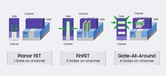
"In the second quarter, the Company aims to expand EUV leadership, beginning with the start of mass production of 5 nm products, while closely monitoring the uncertain market situation caused by COVID-19," the company states in the release. Samsung also announced that following commencement of mass production on 5 nm, further development of GAAFET (gate all-around FET) 3 nanometer silicon fabrication process will get underway. The company appears to be erring on the side of caution with its forward-looking statements, though. Much of what Samsung does will be dictated by the impact of COVID-19 on the supply chain and market.
"In the second quarter, the Company aims to expand EUV leadership, beginning with the start of mass production of 5 nm products, while closely monitoring the uncertain market situation caused by COVID-19," the company states in the release. Samsung also announced that following commencement of mass production on 5 nm, further development of GAAFET (gate all-around FET) 3 nanometer silicon fabrication process will get underway. The company appears to be erring on the side of caution with its forward-looking statements, though. Much of what Samsung does will be dictated by the impact of COVID-19 on the supply chain and market.
5 Comments on Samsung to Commence 5nm EUV Mass-Production in Q2-2020, Develop 3nm GAAFET Node
2020 7nm ampere
2021 7nm ampere refresh
2022 7nm hopper
2023 7nm hopper refersh
2024 5nm nextgen