News Posts matching #GAAFET

Return to Keyword Browsing

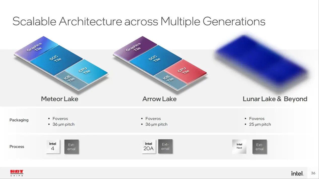
Intel Core Ultra 2-series "Arrow Lake-S" Desktop Features 4 Xe-core iGPU, No Island Cores

Over the weekend, there have been a series of leaks from sources such as Golden Pig Upgrade, and High Yield YT, surrounding Intel's next-generation desktop processor, the Core Ultra 2-series "Arrow Lake-S." The lineup is likely to continue the new client processor naming scheme Intel introduced with the Core Ultra 1-series "Meteor Lake" on the mobile platform. "Arrow Lake-S" is rumored to debut the new Socket LGA1851, which retains cooler-compatibility with LGA1700. Although Intel has nucleated all I/O functions of the traditional PCH to "Meteor Lake," making it a single-chip solution on the mobile platform; and although the mobile "Arrow Lake" will continue to be single-chip; the desktop "Arrow Lake-S" will be a 2-chip solution. This is mainly because the desktop platform demands a lot more PCIe lanes, for a larger number of NVMe storage devices, or high bandwidth devices such as Thunderbolt and USB4 hubs, etc.

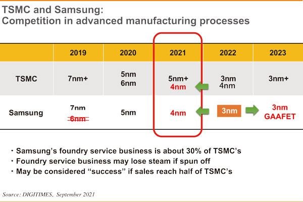
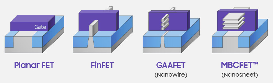
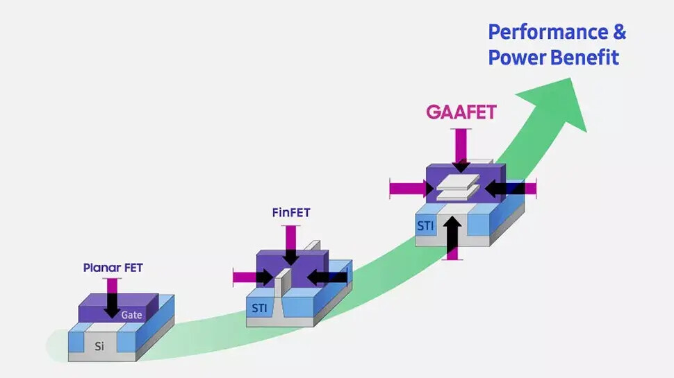
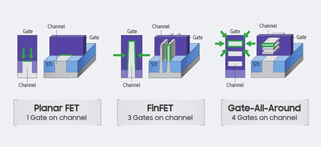
Another key finding in this latest series of leaks, is that unlike "Meteor Lake," the desktop "Arrow Lake-S" will do away with low-power island E-cores located in the SoC tile of the processor. All CPU cores are located in the Compute tile, which is expected to be built in the Intel 20A foundry node—the company's first node to implement GAAFETs (nanosheets), with backside power delivery; as well as an advanced 2nd generation EUV lithography. Intel's 1st Gen EUV is used on the current FinFET-based Intel 4 and Intel 3 foundry nodes.

Samsung Foundry Reportedly Producing 2 nm Prototypes for Qualcomm

Smartphone chipset industry watchdogs believe that the Samsung 3 nm GAA process did not meet customer expectations, due to alleged yield issues. TSMC is seemingly victorious in this segment, as reports suggest that a next-generation 3 nm node production goal of "100,000 monthly wafers by the end of 2024" has been set. Three days ago, Samsung Foundry revealed that it is working on a very advanced SF2 GAAFET process—press outlets in South Korea propose that the manufacturing giant is hoping to outmuscle its main rival in a future 2 nm node category. Tuesday's press introduction stated that a development partnership is set: "to deliver optimized next generation ARM Cortex -X CPU developed on Samsung Foundry's latest Gate-All-Around (GAA) process technology."

A Sedaily article posits that the company's cutting-edge manufacturing tech has already attracted interest from notable parties: "Samsung Electronics is taking advantage of these advantages to win orders for the 2 nm project. Samsung Electronics took its first step by winning an order to produce a 2 nm AI accelerator from Preferred Networks (PFN), Japan's largest AI company. Qualcomm, the world's largest system semiconductor design company, has entered into discussions with Samsung Electronics' System LSI Division, which designs high-performance chips, to produce 2 nm prototypes." December 2023 news reports suggested that Samsung leadership was considering a 2 nm wafer price discount—in order to stay competitive with competing foundry services. It is possible that Qualcomm is evaluating the 2 nm SF2 GAAFET process for a distant Snapdragon 8 "Gen 5" chipset, while Samsung LSI could be working on a 2 nm "Exynos 2600" SoC design.

Samsung Electronics Collaborates with Arm on Optimized Next Gen Cortex-X CPU Using 2nm SF2 GAAFET Process

Samsung Electronics Co., Ltd., a world leader in advanced semiconductor technology, today announced a collaboration to deliver optimized next generation Arm Cortex -X CPU developed on Samsung Foundry's latest Gate-All-Around (GAA) process technology. This initiative is built on years of partnership with millions of devices shipped with Arm CPU intellectual property (IP) on various process nodes offered by Samsung Foundry.

This collaboration sets the stage for a series of announcements and planned innovation between Samsung and Arm. The companies have bold plans to reinvent 2-nanometer (nm) GAA for next-generation data center and infrastructure custom silicon, and a groundbreaking AI chiplet solution that will revolutionize the future generative artificial intelligence (AI) mobile computing market.

TSMC 2 nm Node to Enter Risk Production in Q4-2024, Mass Production in Q2-2025 if All Goes Well

The cutting edge 2 nm EUV foundry node by TSMC is expected to enter risk product in Q4 2024, according to a report by Taiwan-based industry observer DigiTimes. 2 nm would be an important milestone for the foundry company, as it would be the first from the company to implement GAA (gates all around) FETs, the technological successor to FinFETs, which drove silicon fabrication node development for almost a decade, from 16 nm to 3 nm. The GAAFET technology will be critical for the foundry's journey between 2 nm and 1 nm.

TSMC is expected to risk-produce chips on its 2 nm node in its new fab at the Baoshan campus in the Hsinchu Science Park, located in northern Taiwan. Should all go well with risk production, one can expect mass production of chips by Q2-2025. Until then, refinements to the company's final FinFET node, the N3 family, will remain the cutting-edge of silicon fabrication. Samsung has a similar 2025 target set for mass production on its 2 nm node, dubbed SF2. Across the Pacific, Intel Foundry Services has its Intel 20A node, which implements GAAFET (aka RibbonFET) technology aiming for similar timelines, including an ambitious 2024 mass production target.

Intel, TSMC, and Samsung, Demo CFETs at IEEE IEDM Conference, Near Doubling in Transistor Densities in Sight

Last week at the IEEE International Electron Devices Meeting, the world's top-three semiconductor foundries, TSMC, Intel (Intel Foundry Services or IFS), and Samsung Electronics, demonstrated their respective approaches to an evolutionary new transistor device called the CFET, or complementary field-effect transistors. A CFET is a kind of 3-D transistor that stacks both kinds of FETs needed for CMOS logic. All three fabs are transitioning from FinFET to nanosheets, or GAAFETs (gates all-around FETs).

While FinFETs use vertical silicon fins, with gates controlling the flow of current through them; while in a nanosheet, the vertical fin is cut into a set of ribbons, each surrounded by the gate. A CFET is essentially a taller nanosheet device in which uses half of the available ribbons for one device, and the other half for another. This device builds the two types of transistor, nFETs and pFETs on top of each other, in an integrated process. CFETs are the evolutionary next step to conventional GAAFETs, and it's predicted to enter mass production only 7-10 years from now. By that time, the industry will begin to feel the pushback from technological barriers preventing development beyond 10 angstrom-class nodes.

TSMC CFET Transistors in the Lab, Still Many Generations Away

During the European Technology Symposium 2023, TSMC presented additional details regarding the upcoming complementary FET (CFET) technology to power the next generation of silicon-based devices. With Nanosheet replacing FinFET, the CFET technology will do the same to the Gate All Around FET (GAAFET) Nanosheet nodes. As the company notes, CFET transistors are now in the TSMC labs and are being tested for performance, efficiency, and density. Compared to GAAFET, CFET will provide greater design in all of those areas, but it will require some additional manufacturing steps to get the chip working as intended. Integrating both p-type and n-type FETs into a single device, CFET will require the use of High NA EUV scanners with high precision and high power to manufacture it.

The use of CFET, as the roadmap shows, is one of the last steps in the world of silicon. It will require the integration of new materials into the manufacturing process, resulting in a greater investment into research and development that is in charge of node creation. Kevin Zhang, senior vice president at TSMC, responsible for technology roadmap and business development, notes: "Let me make a clarification on that roadmap, everything beyond the Nanosheet is something we will put on our [roadmap] to tell you there is still future out there. We will continue to work on different options. I also have the add on to the one-dimensional material-[based transistors] […], all of those are being researched on being investigated on the future potential candidates right now, we will not tell you exactly the transistor architecture will be beyond the Nanosheet."

US Institutes GAA-FET Technology EDA Software Ban on China, Stalling sub-3nm Nodes

The US Government has instituted a ban on supply of GAA-FET EDA software to China (the Chinese government and companies in China). Humans can no longer design every single circuit on chips with tens of billions of transistors, and so EDA (electronics design automation) software is used to micromanage design based broadly on what chip architects want. Synopsys, Cadence, and Siemens are major EDA software suppliers. Intel is rumored to use an in-house EDA software that it doesn't sell, although this could change with the company roping in third-party foundries, such as TSMC, for cutting-edge logic chips (which will need the software to make sense of Intel's designs).

GAA or "gates-all-around" technology is vital to building transistors in the 3 nm and 2 nm silicon fabrication nodes. Samsung is already using GAA for its 3 nm node, while TSMC intends to use it with its 2N (2 nm) node. Intel is expected to use it with its Intel 20A (20 angstrom, or 2 nanometers) node. Both Intel and TSMC will debut nodes powered by GAAFETs for mass-production in 2024. The US Government has already banned the sales of EUV lithography machines to China, as well as machines fabricating 3D NAND flash chips with greater than 128 layers or 14 nm. In the past, technology embargoes have totally stopped China from copying or reverse-engineering western tech, or luring Taiwanese engineers armed with industry secrets away on the promise of wealth and a comfortable life in the Mainland.

Samsung Working on Attracting more Foundry Customers by Improving Customer Structure and Process Node Breakthroughs

Samsung is by far Samsung's largest foundry customers and this is no secret, but now it seems like the company wants to gain more customers to help pay for the costs of operating a cutting edge foundry. A little over a decade ago, Samsung was part of the Common Platform technology alliance together with GlobalFoundries and IBM, which allowed companies to almost pick either foundry based on a common design kit and common process technologies. It made Samsung an attractive foundry option, but the alliance didn't last.

As we know, Nvidia gave Samsung a try with Ampere and there were a lot of reports of yield issues and what not early on. This seems to have persuaded Nvidia to move back to TSMC for Lovelace and Hopper, which is a big loss for Samsung. However, it seems this was also something of a wakeup call for Samsung, as the company is apparently looking at making some internal changes to its customer structure so it can handle third party customers in a better way.

Samsung 3 nm GAAFET Node Delayed to 2024

Samsung's ambitious 3 nm silicon fabrication node that leverages the Gate All Around FET transistors, has reportedly been delayed to 2024. The company brands this specific node as 3GAE. 2024 is the earliest date when Samsung will be able to mass-produce chips on 3GAE, which means the company, along with Intel, will begin to fall significantly behind TSMC on foundry technology. The Taiwanese semiconductor fabrication giant will target 2 nm-class nodes around 2024, which leverages EUV multi-patterning, extensive use of cobalt in contacts and interconnects, germanium doped channels, and other in-house innovations. With Intel's foundry technology development slowing to a crawl in the sub-10 nm domain, Samsung is the only viable alternative to TSMC for cutting-edge logic chip manufacturing.

Samsung Demonstrates 256 Gb 3 nm MBCFET Chip at ISSCC 2021

During the IEEE International Solid-State Circuits Conference (ISSCC), Samsung Foundry has presented a new step towards smaller and more efficient nodes. The new chip that was presented is a 256 Gb memory chip, based on SRAM technology. However, all of that doesn't sound interesting, until we mention the technology that is behind it. Samsung has for the first time manufactured a chip using the company's gate-all-around field-effect transistor (GAAFET) technology on the 3 nm semiconductor node. Formally, there are two types of GAAFET technology: the regular GAAFET that uses nanowires as fins of the transistor, and MBCFET (multi-bridge channel FET) that uses thicker fins that come in a form of a nanosheet.

Samsung has demonstrated the first SRAM chip that uses MBCFET technology today. The chip in question is a 256 Gb chip with an area of 56 mm². The achievement Samsung is proud of is that the chip uses 230 mV less power for writes, compared to the standard approach, as the MBCFET transistors allow the company to have many different power-saving techniques. The new 3 nm MBCFET process is expected to get into high-volume production sometime in 2022, however, we are yet to see demos of logic chips besides SRAM like we see today. Nonetheless, even the demonstration of SRAM is big progress, and we are eager to see what the company manages to build with the new technology.

Samsung to Build $17 Billion Silicon Manufacturing Plant in the US by 2023

Samsung has been one of the world's biggest foundries and one of three big players still left in the leading-edge semiconductor process development and manufacturing. However, the Korean giant is always seeking ways to improve its offerings, especially for Western customers. Today, it is reported that Samsung has reportedly talked with regulators in Texas, New York, and Arizona about building a $17 billion silicon manufacturing facility in the United States. The supposed factory is going to be located near Austin, Texas, and is supposed to offer around 1800 jobs. If the deal is approved and Samsung manages to complete the project on time, the factory is supposed to start mass production in Q4 of 2023.

What process is Samsung going to manufacture in the new fab? Well, current speculations are pointing out to the 3 nm node, with Samsung's special GAAFET (Gate All Around FET) technology tied to the new node. The fab is also expected to make use of extreme ultraviolet (EUV) lithography for manufacturing. Samsung already has a facility in the US called S2, however, that will not be upgraded as it is still serving a lot of clients. Instead, the company will build new facilities to accommodate the demand for newer nodes. It is important to note that Samsung will not do any R&D work in the new fab, and the company will only manufacture the silicon there.

TSMC Achieves Major Breakthrough in 2 nm Manufacturing Process, Risk Production in 2023

The Taiwan Economic Daily claims that TSMC has achieved a major internal breakthrough for the eventual rollout of 2 nm fabrication process technology. According to the publication, this breakthrough has turned TSMC even more optimistic towards a 2023 rollout of 2 nm risk production - which is all the more impressive considering reports that TSMC will be leaving the FinFet realm for a new multi-bridge channel field effect transistor (MBCFET) architecture - itself based on the Gate-All-Around (GAA) technology. This breakthrough comes one year after TSMC put together an internal team whose aim was to pave the way for 2 nm deployment.

MBCFET expands on the GAAFET architecture by taking the Nanowire field-effect transistor and expanding it so that it becomes a Nanosheet. The main idea is to make the field-effect transistor three-dimensional. This new complementary metal oxide semiconductor transistor can improve circuit control and reduce leakage current. This design philosophy is not exclusive to TSMC - Samsung has plans to deploy a variant of this design on their 3 nm process technology. And as has been the norm, further reductions in chip fabrication scale come at hefty costs - while the development cost for 5 nm has already achieved $476M in cost, Samsung reports that their 3 nm GAA technology will cost in excess of $500M - and 2 nm, naturally, will come in even costlier than that.

Intel Plans to Volume Manufacture Nanowire/Nanoribbon Transistors in Five Years

Semiconductor manufacturing is a hard business. There is a constant need for manufacturers to compete with each other and if they don't, they get left behind. Intel, as one of the biggest semiconductor makers in the world, is always trying to invent new technologies spending massive R&D funds on semiconductors. New technologies such as nanowire/nanoribbon transistors, which are supposed to enable transistor sizes unimaginable now, are on its way to make it in the hand of consumers. During the international VLSI conference, Intel's CTO Mike Mayberry held a presentation about how Intel plans to address the demand for more compute by showing off new technologies.

With a presentation titled "The Future of Compute", Mr. Mayberry made some exciting claims and predictions. So far, we have been used to FinFET transistors since the 22 nm node from Intel. However, as nodes get smaller the gate of the transistor is not enough to keep it from switching randomly. So to avoid that problem Intel, along with other semiconductor manufacturers like Samsung, created a solution called Gate-All-Around FET (GAAFET). This technology takes a transistor fin and wraps in around all sides (see picture below), so the gate has better switching control, preventing random switching and errors. As a fin, nanowire or nanosheet (wider option from nanowire) can be used and they can be stacked. These allow for additional control of tailoring whatever a node will be used for high performance or low power. Intel predicts that they will start high volume manufacturing of silicon based on this technology in five years. This is setting an important milestone for Intel as well as other industry players, as now everyone will rush to deliver it first. It is now a waiting game to see who will actually come out with it first.
Intel Nanowire/Nanoribbon Samsung GAAFET

Samsung to Commence 5nm EUV Mass-Production in Q2-2020, Develop 3nm GAAFET Node

Samsung in its Q1-2020 financials release disclosed that the company will commence mass production of chips on its cutting-edge 5 nanometer EUV silicon fabrication process within Q2-2020 (that's before July 2020). This is big, as it lends credence to rumors of NVIDIA secretly developing 5 nm GPUs. Suddenly, it's possible that "Ampere," if not "Hopper," is 5 nm EUV-based, as NVIDIA has chosen Samsung to be its foundry partner for next-generation GPUs.

"In the second quarter, the Company aims to expand EUV leadership, beginning with the start of mass production of 5 nm products, while closely monitoring the uncertain market situation caused by COVID-19," the company states in the release. Samsung also announced that following commencement of mass production on 5 nm, further development of GAAFET (gate all-around FET) 3 nanometer silicon fabrication process will get underway. The company appears to be erring on the side of caution with its forward-looking statements, though. Much of what Samsung does will be dictated by the impact of COVID-19 on the supply chain and market.

DigiTimes: TSMC Kicking Off Development of 2nm Process Node

A report via DigiTimes places TSMC as having announced to its investors that exploratory studies and R&D for the development of the 2 nm process node have commenced. As today's leading semiconductor fabrication company, TSMC doesn't seem to be one resting on its laurels. Their 7 nm process and derivatives have already achieved a 30% weight on the company's semiconductor orders, and their 5 nm node (which will include EUV litography) is set to hit HVM (High Volume Manufacturing) in Q2 of this year. Apart from that, not much more is known on 2 nm.

After 5 nm, which is expected to boats of an 84-87% transistor density gain over the current 7nm node, the plans are to go 3nm, with TSMC expecting that node to hit mass production come 2022. Interestingly, TSMC is planning to still use FinFET technology for its 3 nm manufacturing node, though in a new GAAFET (gate-all-around field-effect transistor) technology. TSMC's plans to deploy FinFET in under 5nm manufacturing is something that many industry analysts and specialist thought extremely difficult to achieve, with expectations for these sub-5nm nodes to require more exotic materials and transistor designs than TSMC's apparent plans
Return to Keyword Browsing
May 1st, 2024 06:55 EDT change timezone

New Forum Posts

Popular Reviews

Controversial News Posts