Friday, March 12th 2021

Samsung Demonstrates 256 Gb 3 nm MBCFET Chip at ISSCC 2021
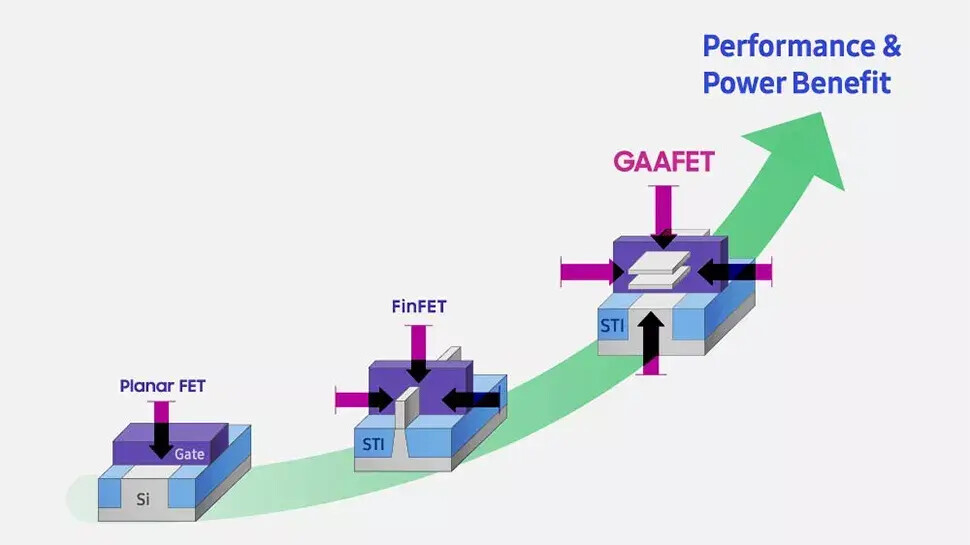
During the IEEE International Solid-State Circuits Conference (ISSCC), Samsung Foundry has presented a new step towards smaller and more efficient nodes. The new chip that was presented is a 256 Gb memory chip, based on SRAM technology. However, all of that doesn't sound interesting, until we mention the technology that is behind it. Samsung has for the first time manufactured a chip using the company's gate-all-around field-effect transistor (GAAFET) technology on the 3 nm semiconductor node. Formally, there are two types of GAAFET technology: the regular GAAFET that uses nanowires as fins of the transistor, and MBCFET (multi-bridge channel FET) that uses thicker fins that come in a form of a nanosheet.
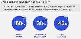
Samsung has demonstrated the first SRAM chip that uses MBCFET technology today. The chip in question is a 256 Gb chip with an area of 56 mm². The achievement Samsung is proud of is that the chip uses 230 mV less power for writes, compared to the standard approach, as the MBCFET transistors allow the company to have many different power-saving techniques. The new 3 nm MBCFET process is expected to get into high-volume production sometime in 2022, however, we are yet to see demos of logic chips besides SRAM like we see today. Nonetheless, even the demonstration of SRAM is big progress, and we are eager to see what the company manages to build with the new technology.
Source:
Tom's Hardware
Samsung has demonstrated the first SRAM chip that uses MBCFET technology today. The chip in question is a 256 Gb chip with an area of 56 mm². The achievement Samsung is proud of is that the chip uses 230 mV less power for writes, compared to the standard approach, as the MBCFET transistors allow the company to have many different power-saving techniques. The new 3 nm MBCFET process is expected to get into high-volume production sometime in 2022, however, we are yet to see demos of logic chips besides SRAM like we see today. Nonetheless, even the demonstration of SRAM is big progress, and we are eager to see what the company manages to build with the new technology.

15 Comments on Samsung Demonstrates 256 Gb 3 nm MBCFET Chip at ISSCC 2021
This mainly demonstrates that Samsung is well on the way to implementing 3nm MBCFET for actual products, though I'd be surprised if anything started volume production in less than a year.
Samsung 3nm GAA has 216.37 MTr/mm², so the total size of a single transistor could be something like 68×68 nm, on average. Big, hah?
And the SRAM cell size (6 transistors) is 0.0187 µm², so like 136×136 nm.
Transistor size varies A LOT between different structures, and while logic shrinks very well with each new node, SRAM shrinks quite poorly. For those interested, there's an excellent discussion about that on Real World Tech: Transistor Count - A Flawed Metric
The purpose of this first chip (not just one, my guess is it was a small batch of wafers) is characteriation, anyway. Samsung needs to know exactly what they have produced using mass-manufacturing tools. They need to determine the electrical characteristics of the new transistors and how much they vary within a chip, a wafer, and a batch. The result is a large bunch of data and graphs, like those presented here, that to chip designers mean everything.
In the case of FinFET in order to increase speed you need to place multiple Fins next to each other which takes space horizontally ( which most of the time is not possible ) furthermore this is where double , triple or quadruple patterning ( depending the lithography envolved ) comes to play and this is what is referred to as '' additional processing steps " which adds cost .
On the other hand in the case of MBCFET the Nanosheets ( which replace the fins ) can be stacked vertically , so speed can be increased without any compromise being made to the footprint . Furthermore those Nanosheets are much larger than Fins which should minimise the need for multi-patterning if not eliminate it and thus driving complexity and cost down .
www.tomshardware.fr/content/uploads/sites/3/2019/05/mbcfet-samsung.jpg
Reduced complexity and cost are nowhere in sight here. Rather, there are no other options for the foreseeable future.