News Posts matching #GAA

Return to Keyword Browsing

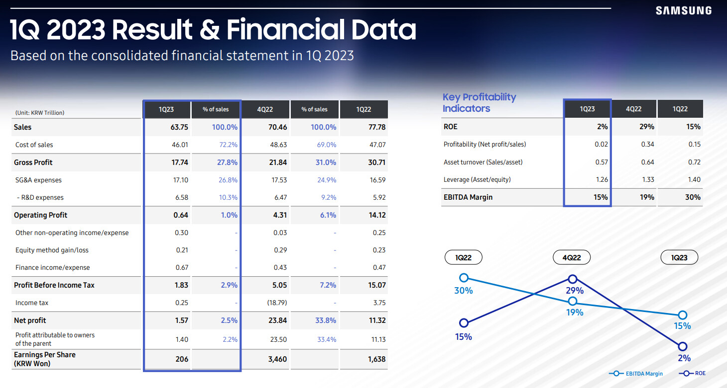
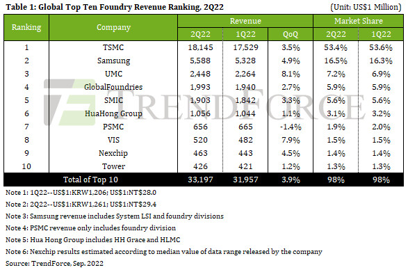
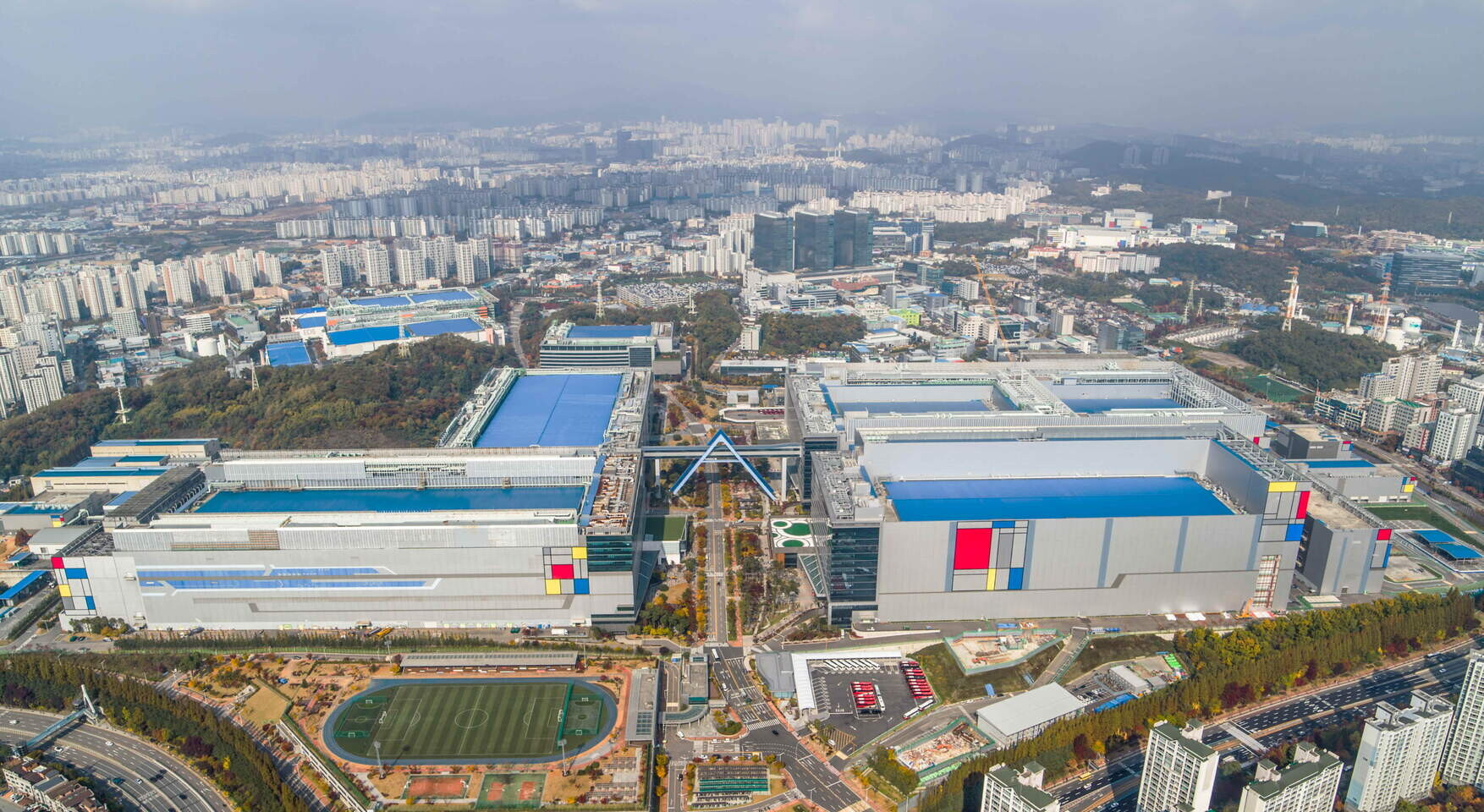
Samsung Foundry Renames 3 nm Process to 2 nm Amid Competition with Intel

In a move that could intensify competition with Intel in the cutting-edge chip manufacturing space, Samsung Foundry has reportedly decided to rebrand its second-generation 3 nm-class fabrication technology, previously known as SF3, to a 2 nm-class manufacturing process called SF2. According to reports from ZDNet, the renaming of Samsung's SF3 to SF2 is likely an attempt by the South Korean tech giant to simplify its process nomenclature and better compete against Intel Foundry, at least visually. Intel is set to roll out its Intel 20A production node, a 2 nm-class technology, later this year. The reports suggest that Samsung has already notified its customers about the changes in its roadmap and the renaming of SF3 to SF2. Significantly, the company has reportedly gone as far as re-signing contracts with customers initially intended to use the SF3 production node.

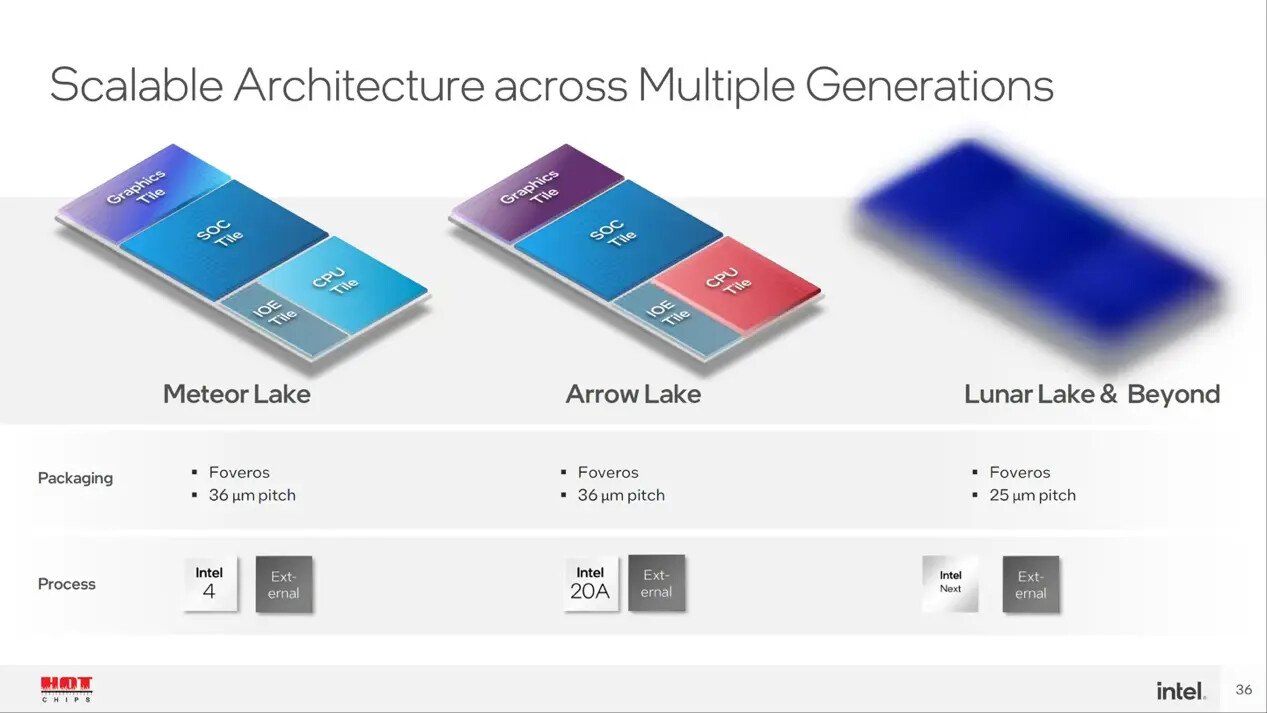
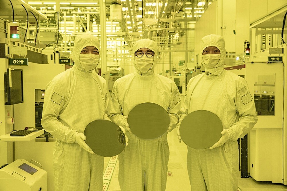
"We were informed by Samsung Electronics that the 2nd generation 3 nm [name] is being changed to 2 nm," an unnamed source noted to ZDNet. "We had contracted Samsung Foundry for the 2nd generation 3 nm production last year, but we recently revised the contract to change the name to 2 nm." Despite the name change, Samsung's SF3, now called SF2, has not undergone any actual process technology alterations. This suggests that the renaming is primarily a marketing move, as using a different process technology would require customers to rework their chip designs entirely. Samsung intends to start manufacturing chips based on the newly named SF2 process in the second half of 2024. The SF2 technology, which employs gate-all-around (GAA) transistors that Samsung brands as Multi-Bridge-Channel Field Effect Transistors (MBCFET), does not feature a backside power delivery network (BSPDN), a significant advantage of Intel's 20A process. Samsung Foundry has not officially confirmed the renaming.

Intel Core Ultra 2-series "Arrow Lake-S" Desktop Features 4 Xe-core iGPU, No Island Cores

Over the weekend, there have been a series of leaks from sources such as Golden Pig Upgrade, and High Yield YT, surrounding Intel's next-generation desktop processor, the Core Ultra 2-series "Arrow Lake-S." The lineup is likely to continue the new client processor naming scheme Intel introduced with the Core Ultra 1-series "Meteor Lake" on the mobile platform. "Arrow Lake-S" is rumored to debut the new Socket LGA1851, which retains cooler-compatibility with LGA1700. Although Intel has nucleated all I/O functions of the traditional PCH to "Meteor Lake," making it a single-chip solution on the mobile platform; and although the mobile "Arrow Lake" will continue to be single-chip; the desktop "Arrow Lake-S" will be a 2-chip solution. This is mainly because the desktop platform demands a lot more PCIe lanes, for a larger number of NVMe storage devices, or high bandwidth devices such as Thunderbolt and USB4 hubs, etc.

Another key finding in this latest series of leaks, is that unlike "Meteor Lake," the desktop "Arrow Lake-S" will do away with low-power island E-cores located in the SoC tile of the processor. All CPU cores are located in the Compute tile, which is expected to be built in the Intel 20A foundry node—the company's first node to implement GAAFETs (nanosheets), with backside power delivery; as well as an advanced 2nd generation EUV lithography. Intel's 1st Gen EUV is used on the current FinFET-based Intel 4 and Intel 3 foundry nodes.

Samsung Foundry Reportedly Producing 2 nm Prototypes for Qualcomm

Smartphone chipset industry watchdogs believe that the Samsung 3 nm GAA process did not meet customer expectations, due to alleged yield issues. TSMC is seemingly victorious in this segment, as reports suggest that a next-generation 3 nm node production goal of "100,000 monthly wafers by the end of 2024" has been set. Three days ago, Samsung Foundry revealed that it is working on a very advanced SF2 GAAFET process—press outlets in South Korea propose that the manufacturing giant is hoping to outmuscle its main rival in a future 2 nm node category. Tuesday's press introduction stated that a development partnership is set: "to deliver optimized next generation ARM Cortex -X CPU developed on Samsung Foundry's latest Gate-All-Around (GAA) process technology."

A Sedaily article posits that the company's cutting-edge manufacturing tech has already attracted interest from notable parties: "Samsung Electronics is taking advantage of these advantages to win orders for the 2 nm project. Samsung Electronics took its first step by winning an order to produce a 2 nm AI accelerator from Preferred Networks (PFN), Japan's largest AI company. Qualcomm, the world's largest system semiconductor design company, has entered into discussions with Samsung Electronics' System LSI Division, which designs high-performance chips, to produce 2 nm prototypes." December 2023 news reports suggested that Samsung leadership was considering a 2 nm wafer price discount—in order to stay competitive with competing foundry services. It is possible that Qualcomm is evaluating the 2 nm SF2 GAAFET process for a distant Snapdragon 8 "Gen 5" chipset, while Samsung LSI could be working on a 2 nm "Exynos 2600" SoC design.

Samsung Electronics Collaborates with Arm on Optimized Next Gen Cortex-X CPU Using 2nm SF2 GAAFET Process

Samsung Electronics Co., Ltd., a world leader in advanced semiconductor technology, today announced a collaboration to deliver optimized next generation Arm Cortex -X CPU developed on Samsung Foundry's latest Gate-All-Around (GAA) process technology. This initiative is built on years of partnership with millions of devices shipped with Arm CPU intellectual property (IP) on various process nodes offered by Samsung Foundry.

This collaboration sets the stage for a series of announcements and planned innovation between Samsung and Arm. The companies have bold plans to reinvent 2-nanometer (nm) GAA for next-generation data center and infrastructure custom silicon, and a groundbreaking AI chiplet solution that will revolutionize the future generative artificial intelligence (AI) mobile computing market.

Intel Reports Fourth-Quarter and Full-Year 2023 Financial Results

Intel Corporation today reported fourth-quarter and full-year 2023 financial results. "We delivered strong Q4 results, surpassing expectations for the fourth consecutive quarter with revenue at the higher end of our guidance," said Pat Gelsinger, Intel CEO. "The quarter capped a year of tremendous progress on Intel's transformation, where we consistently drove execution and accelerated innovation, resulting in strong customer momentum for our products. In 2024, we remain relentlessly focused on achieving process and product leadership, continuing to build our external foundry business and at-scale global manufacturing, and executing our mission to bring AI everywhere as we drive long-term value for stakeholders."

David Zinsner, Intel CFO, said, "We continued to drive operational efficiencies in the fourth quarter, and comfortably achieved our commitment to deliver $3 billion in cost savings in 2023. We expect to unlock further efficiencies in 2024 and beyond as we implement our new internal foundry model, which is designed to drive greater transparency and accountability and higher returns on our owners' capital." For the full year, the company generated $11.5 billion in cash from operations and paid dividends of $3.1 billion.

Intel Demos 3D Transistors, RibbonFET, and PowerVia Technologies

During the 69th annual IEEE International Electron Devices Meeting (IEDM), Intel demonstrated some of its latest transistor design and manufacturing advancements. The first one in line is the 3D integration of transistors. According to Intel, the company has successfully stacked complementary field effect transistors (CFET) at a scaled gate pitch down to 60 nm. With CFETs promising thinner gate channels, the 3D stacked CFET would allow for higher density by going vertically and horizontally. Intel's 7 node has a 54 nm gate pitch, meaning CFETs are already close to matching production-ready nodes. With more time and development, we expect to see 3D stacked CFETs in the production runs in the coming years.

Next, Intel has demonstrated RibbonFET technology, a novel approach that is the first new transistor architecture since the introduction of FinFET in 2012. Using ribbon-shaped channels surrounded by the gate, these transistors allow for better control and higher drive current at all voltage levels. This allows faster transistor switching speeds, which later lead to higher frequency and performance. The width of these nanoribbon channels can be modulated depending on the application, where low-power mobile applications use less current, making the channels thinner, and high-performance applications require more current, making the channels wider. One stack of nanoribbons can achieve the same drive current as multiple fins found in FinFET but at a smaller footprint.

Samsung and TSMC Reportedly Struggling with 3 nm Yields

According to Korean business news publication ChosunBiz, both Samsung and TSMC are struggling with their 3 nm node yields. The two companies have different approaches to their 3 nm nodes, with Samsung using GAA FET (Gate All Around), whereas TSMC is continuing with its FinFET technology. That said, TSMC has at least five known 3 nm nodes, of which two should be in production by now, assuming N3E has proved to be reliable enough to kick off. Samsung on the other hand has three known 3 nm nodes, with only one in production so far, called 3GAE.

ChosunBiz reports that neither company is getting the kind of yields that you'd expect from a node that should have been in volume production for around a year by now, with Samsung apparently being somewhat better than TSMC. At 60 and 50 percent respectively, neither Samsung nor TSMC are anywhere near decent yields. Anything below 70 percent is considered very poor and even the 60 percent claim in Samsungs case, is apparently limited to some kind of Chinese mining ASIC and doesn't include the SRAM you find in most modern processors. ChosunBiz also mentions a source familiar with Samsung's foundry business who mentions a yield closer to 50 percent for the company. The same source also mentions that Samsung needs to reach at least 70 percent yield to be able to attract major customers to its 3 nm node.

TSMC Could Delay 2 nm Mass Production to 2026

According to TechNews.tw, TSMC could postpone its 2 nm semiconductor manufacturing node for 2026. If the rumors about TSMC's delayed 2 nm production schedule are accurate, the implications could reverberate throughout the semiconductor industry. TSMC's alleged hesitancy could be driven by multiple factors, including the architectural shift from FinFET to Gate-All-Around (GAA) and potential challenges related to scaling down to 2 nm. The company is a crucial player in this space, and a delay could offer opportunities for competitors like Samsung, which has already transitioned to GAA transistor architecture for its 3 nm chips. Given the massive demand for advanced nodes due to the rise of AI, IoT, and other next-gen technologies, it is surprising to hear "sluggish" demand reports.

However, it's also possible that it's too early for customers to make firm commitments for 2025 and beyond. TSMC has dismissed these rumors, stating that construction is progressing according to plan, which includes having 2 nm pilot run in 2024, and mass production in the second half of 2025.. Despite this, any delay in TSMC's roadmap could serve as a catalyst for shifts in market dynamics. Companies that rely heavily on TSMC's advanced nodes might need to reassess their timelines and strategies. Moreover, if Samsung can capitalize on this opportunity, it could somewhat level the playing field. As of now, though, it's essential to approach these rumors with caution until more concrete information becomes available.

Samsung Electronics Announces Second Quarter 2023 Results

Samsung Electronics today reported financial results for the second quarter ended June 30, 2023. The Company posted KRW 60.01 trillion in consolidated revenue, a 6% decline from the previous quarter, mainly due to a decline in smartphone shipments despite a slight recovery in revenue of the DS (Device Solutions) Division. Operating profit rose sequentially to KRW 0.67 trillion as the DS Division posted a narrower loss, while Samsung Display Corporation (SDC) and the Digital Appliances Business saw improved profitability.

The Memory Business saw results improve from the previous quarter as its focus on High Bandwidth Memory (HBM) and DDR5 products in anticipation of robust demand for AI applications led to higher-than-guided DRAM shipments. System semiconductors posted a decline in profit due to lower utilization rates on weak demand from major applications.

Samsung's 3 nm GAA Process Identified in a Crypto-mining ASIC Designed by China Startup MicroBT

Semiconductor industry research firm TechInsights said it has found that Samsung's 3 nm GAA (gate-all-around) process has been incorporated into the crypto miner ASIC (Whatsminer M56S++) from a Chinese manufacturer, MicroBT. In a Disruptive Technology Event Brief exclusively provided to DIGITIMES Asia, TechInsights points out that the significance of this development lies in the commercial utilization of GAA technology, which facilitates the scaling of transistors to 2 nm and beyond. "This development is crucial because it has the potential to enhance performance, improve energy efficiency, keep up with Moore's Law, and enable advanced applications," said TechInsights, identifying the MicroBT ASIC chip the first commercialized product using GAA technology in the industry.

But this would also reveal that Samsung is the foundry for MicroBT, using the 3 nm GAA process. DIGITIMES Research semiconductor analyst Eric Chen pointed out that Samsung indeed has started producing chips using the 3 nm GAA process, but the capacity is still small. "Getting revenues from shipment can be defined as 'commercialization', but ASIC is a relatively simple kind of chip to produce, in terms of architecture."

Samsung Claims Higher 3 nm Yields than TSMC

Competition between Samsung and TSMC in the 4 nm and 3 nm foundry process markets is about to heat up, with the Korean foundry claiming yields competitive to those of TSMC, according to a report in the Kukmin Ilbo, a Korean daily newspaper. 4 nm is the final silicon fabrication process to use the FinFET technology that powered nodes ranging between 16 nm to 4 nm. Samsung Foundry is claiming 4 nm wafer yields of 75%, against the 80% yields figure put out by TSMC. 4 nm powers several current-generation mobile SoCs, PC processors, and more importantly, the GPUs driving the AI gold-rush.

Things get very interesting with 3 nm, the node that debuts GAA-FET (gates all around FET) technology. Here, Samsung claims to offer higher yields than TSMC, with its 3 nm GAA node clocking 60% yields, against 55% put out by TSMC. Samsung was recently bitten by a scandal where its engineers allegedly falsified yields figures to customers to score orders, which had a cascading effect on the volumes and competitiveness of their customers. We're inclined to think that Samsung has taken lessons and is more careful with the yields figures being reported in the press. Meanwhile, Intel Foundry Services competes with the Intel 3 node, which is physically 7 nm FinFET, but with electrical characteristics comparable to those of 3 nm.

TSMC Said to Start Construction of 1.4 nm Fab in 2026

According to Taiwanese media, TSMC will start production of its first 1.4 nm fab in 2026, with chip production in the fab said to start sometime in 2027 or 2028. The new fab will be located in Longtan Science Park outside of Hsinchu in Taiwan, where many of TSMC's current fabs are located. TSMC is currently constructing a 2 nm and below node R&D facility at a nearby plot of land to where the new fab is expected to be built. This facility is expected to be finished in 2025 and TSMC has been allocated a total area of just over 158 hectares of land for future expansion in the area.

In related news, TSMC is expected to be charging US$25,000 per 2 nm GAA wafer, which is an increase of about a fifth compared to its 3 nm wafers which are going for around US$20,000. This is largely due to the nodes being fully booked and TSMC being able to charge a premium for its cutting edge nodes. TSMC is also expanding in CoWoS packaging facilities due to increased demand from both AMD and NVIDIA for AI related products. Currently TSMC is said to be able to output 12,000 CoWoS wafers per month and this is twice as much as last year, yet TSMC is unable to meet demand from its customers.

Samsung Electronics Unveils Foundry Vision in the AI Era

Samsung Electronics, a world leader in advanced semiconductor technology, today announced its latest foundry technology innovations and business strategy at the 7th annual Samsung Foundry Forum (SFF) 2023. Under the theme "Innovation Beyond Boundaries," this year's forum delved into Samsung Foundry's mission to address customer needs in the artificial intelligence (AI) era through advanced semiconductor technology.

Over 700 guests, from customers and partners of Samsung Foundry, attended this year's event, of which 38 companies hosted their own booths to share the latest technology trends in the foundry industry.

TSMC CFET Transistors in the Lab, Still Many Generations Away

During the European Technology Symposium 2023, TSMC presented additional details regarding the upcoming complementary FET (CFET) technology to power the next generation of silicon-based devices. With Nanosheet replacing FinFET, the CFET technology will do the same to the Gate All Around FET (GAAFET) Nanosheet nodes. As the company notes, CFET transistors are now in the TSMC labs and are being tested for performance, efficiency, and density. Compared to GAAFET, CFET will provide greater design in all of those areas, but it will require some additional manufacturing steps to get the chip working as intended. Integrating both p-type and n-type FETs into a single device, CFET will require the use of High NA EUV scanners with high precision and high power to manufacture it.

The use of CFET, as the roadmap shows, is one of the last steps in the world of silicon. It will require the integration of new materials into the manufacturing process, resulting in a greater investment into research and development that is in charge of node creation. Kevin Zhang, senior vice president at TSMC, responsible for technology roadmap and business development, notes: "Let me make a clarification on that roadmap, everything beyond the Nanosheet is something we will put on our [roadmap] to tell you there is still future out there. We will continue to work on different options. I also have the add on to the one-dimensional material-[based transistors] […], all of those are being researched on being investigated on the future potential candidates right now, we will not tell you exactly the transistor architecture will be beyond the Nanosheet."

Samsung Claims 60-70% Yields for its 3 nm Node

Samsung Electronics is engaged in stiff competition with TSMC for chip manufacturing orders for 3 nm, its first semiconductor foundry node to implement GAA-FET technology, after nearly a decade of FinFET-based nodes. SF3, a 3 nm GAA-FET node, enters mass-production later this year. Samsung is claiming wafer yields in the range of 60-70% in the development phases of the node. This number is crucial to attract customers as they base their wafer orders squarely on yields first, and cost-per-wafer next.

Samsung is trying to rebuild confidence among chip designers after the 2022 controversy over its engineering "fabricating" yield numbers to customers to win their business. Samsung also stated that with 2023-2024 being dominated by 3 nm-class nodes, namely SF3 (3GAP), and its refinement the SF3P (3GAP+), the company will begin introducing its 2 nm class nodes in 2025-2026. Samsung's current customers for its 3 nm node include unnamed HPC processor designer, and a mobile AP (application processor) designer.

Samsung Electronics Announces First Quarter 2023 Results, Profits Lowest in 14 Years

Samsung Electronics today reported financial results for the first quarter ended March 31, 2023. The Company posted KRW 63.75 trillion in consolidated revenue, a 10% decline from the previous quarter, as overall consumer spending slowed amid the uncertain global macroeconomic environment. Operating profit was KRW 0.64 trillion as the DS (Device Solutions) Division faced decreased demand, while profit in the DX (Device eXperience) Division increased.

The DS Division's profit declined from the previous quarter due to weak demand in the Memory Business, a decline in utilization rates in the Foundry Business and continued weak demand and inventory adjustments from customers. Samsung Display Corporation (SDC) saw earnings in the mobile panel business decline quarter-on-quarter amid a market contraction, while the large panel business slightly narrowed its losses. The DX Division's results improved on the back of strong sales of the premium Galaxy S23 series as well as an enhanced sales mix focusing on premium TVs.

Intel Foundry and Arm Announce Multigeneration Collaboration on Leading-Edge SoC Design

Intel Foundry Services (IFS) and Arm today announced a multigeneration agreement to enable chip designers to build low-power compute system-on-chips (SoCs) on the Intel 18A process. The collaboration will focus on mobile SoC designs first, but allow for potential design expansion into automotive, Internet of Things (IoT), data center, aerospace and government applications. Arm customers designing their next-generation mobile SoCs will benefit from leading-edge Intel 18A process technology, which delivers new breakthrough transistor technologies for improved power and performance, and from IFS's robust manufacturing footprint that includes U.S.- and EU-based capacity.

"There is growing demand for computing power driven by the digitization of everything, but until now fabless customers have had limited options for designing around the most advanced mobile technology," said Pat Gelsinger, CEO of Intel Corporation. "Intel's collaboration with Arm will expand the market opportunity for IFS and open up new options and approaches for any fabless company that wants to access best-in-class CPU IP and the power of an open system foundry with leading-edge process technology."

Intel 20A and 18A Foundry Nodes Complete Development Phase, On Track for 2024 Manufacturing

Intel Foundry Services, the in-house semiconductor foundry of Intel, announced that its 2 nm-class Intel 20A and 1.8 nm-class Intel 18A foundry nodes have completed development, and are on course for mass-producing chips on their roadmap dates. Chips are expected to begin mass-production on the Intel 20A node in the first half of 2024, while those on the Intel 18A node are expected to begin in the second half of 2024. The completion of the development phase means that Intel has finalized the specifications and performance/power targets of the nodes, the tools and software required to make the chips, and can now begin ordering them to build the nodes. Intel has been testing these nodes through 2022, and with the specs being finalized, chip-designers can accordingly wrap up development of their products to align with what these nodes have to offer.

Intel 20A (or 20-angstrom, or 2 nm) node introduces gates-all-around (GAA) RibbonFET transistors with PowerVIAs (an interconnect innovation that contributes to transistor densities). The Intel 20A node is claimed to offer a 15% performance/Watt gain over its predecessor, the Intel 3 node (FinFET EUV, 3 nm-class), which by itself offers an 18% performance/Watt gain over Intel 4 (20% perf/Watt gain over the current Intel 7 node), the node that is entering mass-production very soon. The Intel 18A node is a further refinement of Intel 20A, and introduces a design improvement to the RibbonFET that increases transistor density at scale, and a claimed 10% performance/Watt improvement over Intel 20A.

Samsung Electronics Announces Fourth Quarter and FY 2022 Results, Profits at an 8-year Low

Samsung Electronics today reported financial results for the fourth quarter and the fiscal year 2022. The Company posted KRW 70.46 trillion in consolidated revenue and KRW 4.31 trillion in operating profit in the quarter ended December 31, 2022. For the full year, it reported 302.23 trillion in annual revenue, a record high and KRW 43.38 trillion in operating profit.

The business environment deteriorated significantly in the fourth quarter due to weak demand amid a global economic slowdown. Earnings at the Memory Business decreased sharply as prices fell and customers continued to adjust inventory. The System LSI Business also saw a decline in earnings as sales of key products were weighed down by inventory adjustments in the industry. The Foundry Business posted a new record for quarterly revenue while profit increased year-on-year on the back of advanced node capacity expansion as well as customer base and application area diversification.

Intel Research Fuels Moore's Law and Paves the Way to a Trillion Transistors by 2030

Today, Intel unveiled research breakthroughs fueling its innovation pipeline for keeping Moore's Law on track to a trillion transistors on a package in the next decade. At IEEE International Electron Devices Meeting (IEDM) 2022, Intel researchers showcased advancements in 3D packaging technology with a new 10x improvement in density; novel materials for 2D transistor scaling beyond RibbonFET, including super-thin material just 3 atoms thick; new possibilities in energy efficiency and memory for higher-performing computing; and advancements for quantum computing.

"Seventy-five years since the invention of the transistor, innovation driving Moore's Law continues to address the world's exponentially increasing demand for computing. At IEDM 2022, Intel is showcasing both the forward-thinking and concrete research advancements needed to break through current and future barriers, deliver to this insatiable demand, and keep Moore's Law alive and well for years to come." -Gary Patton, Intel vice president and general manager of Components Research and Design Enablement

AMD Trims Q3 Forecast, $1 Billion Missing, Client Processor Revenue down 40%, Halved Quarter-over-Quarter

AMD (NASDAQ:AMD) today announced selected preliminary financial results for the third quarter of 2022. Third quarter revenue is expected to be approximately $5.6 billion, an increase of 29% year-over-year. AMD previously expected revenue to increase approximately 55% year-over-year at the mid-point of guidance. Preliminary results reflect lower than expected Client segment revenue resulting from reduced processor shipments due to a weaker than expected PC market and significant inventory correction actions across the PC supply chain.

Revenue for the Data Center, Gaming, and Embedded segments each increased significantly year-over-year in-line with the company's expectations. Gross margin is expected to be approximately 42% and non-GAAP(*) gross margin is expected to be approximately 50%. AMD previously expected non-GAAP gross margin to be approximately 54%. The gross margin shortfall to expectations was primarily due to lower revenue driven by lower Client processor unit shipments and average selling price (ASP). In addition, the third quarter results are expected to include approximately $160 million of charges primarily for inventory, pricing, and related reserves in the graphics and client businesses.

Samsung Electronics Unveils Plans for 1.4 nm Process Technology

Samsung Electronics, a world leader in advanced semiconductor technology, announced today a strengthened business strategy for its Foundry Business with the introduction of cutting-edge technologies at its annual Samsung Foundry Forum event. With significant market growth in high-performance computing (HPC), artificial intelligence (AI), 5/6G connectivity and automotive applications, demand for advanced semiconductors has increased dramatically, making innovation in semiconductor process technology critical to the business success of foundry customers. To that end, Samsung highlighted its commitment to bringing its most advanced process technology, 1.4-nanometer (nm), for mass production in 2027.

During the event, Samsung also outlined steps its Foundry Business is taking in order to meet customers' needs, including: foundry process technology innovation, process technology optimization for each specific applications, stable production capabilities, and customized services for customers. "The technology development goal down to 1.4 nm and foundry platforms specialized for each application, together with stable supply through consistent investment are all part of Samsung's strategies to secure customers' trust and support their success," said Dr. Si-young Choi, president and head of Foundry Business at Samsung Electronics. "Realizing every customer's innovations with our partners has been at the core of our foundry service."

2Q22 Output Value Growth at Top 10 Foundries Falls to 3.9% QoQ, Says TrendForce

According to TrendForce research, due to steady weakening of overall demand for consumer electronics, inventory pressure has increased among downstream distributors and brands. Although there are still sporadic shortages of specific components, the curtain has officially fallen on a two-year wave of shortages in general, and brands have gradually suspended stocking in response to changes in market conditions. However, stable demand for automotive and industrial equipment is key to supporting the ongoing growth of foundry output value. At the same time, since the creation of a marginal amount of new capacity in 2Q22 led to growth in wafer shipments and a price hike for certain wafers, this drove output value among top ten foundries to reach US$33.20 billion in 2Q22. Quarterly growth fell to 3.9% on a weakening consumer market.

A prelude to inventory correction was officially revealed in 3Q22. In addition to intensifying severity in the initial wave of order slashing for LDDI/TDDI, and TV SoC, diminishing order volume also extended to non-Apple smartphone APs and peripheral IC PMIC, CIS, and consumer electronics PMICs, and mid-to-low-end MCUs, posing a challenge for foundry capacity utilization. However, the launch of the new iPhone in 3Q22 is expected to prop up a certain amount of stocking momentum for the sluggish market. Therefore, top ten foundry revenue in 3Q22 is expected to maintain a growth trend driven by high-priced processes and quarterly growth rate is expected to be slightly higher than in 2Q22.

Microsoft Cloud strength drives fourth quarter results

Microsoft Corp. today announced the following results for the quarter ended June 30, 2022, as compared to the corresponding period of last fiscal year:
  • Revenue was $51.9 billion and increased 12% (up 16% in constant currency)
  • Operating income was $20.5 billion and increased 8% (up 14% in constant currency)
  • Net income was $16.7 billion and increased 2% (up 7% in constant currency)
  • Diluted earnings per share was $2.23 and increased 3% (up 8% in constant currency)
"We see real opportunity to help every customer in every industry use digital technology to overcome today's challenges and emerge stronger," said Satya Nadella, chairman and chief executive officer of Microsoft. "No company is better positioned than Microsoft to help organizations deliver on their digital imperative - so they can do more with less."

Samsung Begins Chip Production Using 3nm Process Technology With GAA Architecture

Samsung Electronics, the world leader in semiconductor technology, today announced that it has started initial production of its 3-nanometer (nm) process node applying Gate-All-Around (GAA) transistor architecture. Multi-Bridge-Channel FET (MBCFET), Samsung's GAA technology implemented for the first time ever, defies the performance limitations of FinFET, improving power efficiency by reducing the supply voltage level, while also enhancing performance by increasing drive current capability. Samsung is starting the first application of the nanosheet transistor with semiconductor chips for high performance, low power computing application and plans to expand to mobile processors.

"Samsung has grown rapidly as we continue to demonstrate leadership in applying next-generation technologies to manufacturing, such as foundry industry's first High-K Metal Gate, FinFET, as well as EUV. We seek to continue this leadership with the world's first 3 nm process with the MBCFET," said Dr. Siyoung Choi, President and Head of Foundry Business at Samsung Electronics. "We will continue active innovation in competitive technology development and build processes that help expedite achieving maturity of technology."
Return to Keyword Browsing
Apr 30th, 2024 23:17 EDT change timezone

New Forum Posts

Popular Reviews

Controversial News Posts