Thursday, June 30th 2022

Samsung Begins Chip Production Using 3nm Process Technology With GAA Architecture
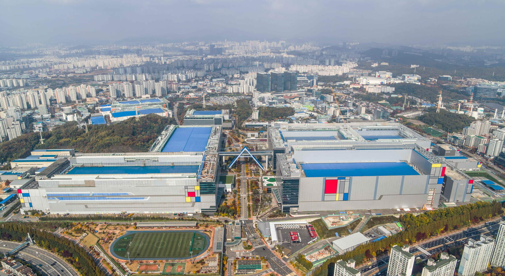
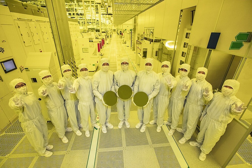
Samsung Electronics, the world leader in semiconductor technology, today announced that it has started initial production of its 3-nanometer (nm) process node applying Gate-All-Around (GAA) transistor architecture. Multi-Bridge-Channel FET (MBCFET), Samsung's GAA technology implemented for the first time ever, defies the performance limitations of FinFET, improving power efficiency by reducing the supply voltage level, while also enhancing performance by increasing drive current capability. Samsung is starting the first application of the nanosheet transistor with semiconductor chips for high performance, low power computing application and plans to expand to mobile processors.
"Samsung has grown rapidly as we continue to demonstrate leadership in applying next-generation technologies to manufacturing, such as foundry industry's first High-K Metal Gate, FinFET, as well as EUV. We seek to continue this leadership with the world's first 3 nm process with the MBCFET," said Dr. Siyoung Choi, President and Head of Foundry Business at Samsung Electronics. "We will continue active innovation in competitive technology development and build processes that help expedite achieving maturity of technology."


 Design-Technology Optimization for Maximized PPA
Samsung's proprietary technology utilizes nanosheets with wider channels, which allow higher performance and greater energy efficiency compared to GAA technologies using nanowires with narrower channels. Utilizing the 3 nm GAA technology, Samsung will be able to adjust the channel width of the nanosheet in order to optimize power usage and performance to meet various customer needs.
In addition, the design flexibility of GAA is highly advantageous for Design Technology Co-Optimization (DTCO), which helps boost Power, Performance, Area (PPA) benefits. Compared to 5 nm process, the first-generation 3 nm process can reduce power consumption by up to 45%, improve performance by 23% and reduce area by 16% compared to 5 nm, while the second-generation 3 nm process is to reduce power consumption by up to 50%, improve performance by 30% and reduce area by 35%.
Providing 3 nm Design Infrastructure & Services With SAFE Partners
As technology nodes get smaller and chip performance needs grow greater, IC designers face challenges of handling tremendous amounts of data to verify complex products with more functions and tighter scaling. To meet such demands, Samsung strives to provide a more stable design environment to help reduce the time required for design, verification and sign-off process, while also boosting product reliability.
Since the third quarter of 2021, Samsung Electronics has been providing proven design infrastructure through extensive preparation with Samsung Advanced Foundry Ecosystem (SAFE ) partners including Ansys, Cadence, Siemens and Synopsys, to help customers perfect their product in a reduced period of time.
Source:
Samsung
"Samsung has grown rapidly as we continue to demonstrate leadership in applying next-generation technologies to manufacturing, such as foundry industry's first High-K Metal Gate, FinFET, as well as EUV. We seek to continue this leadership with the world's first 3 nm process with the MBCFET," said Dr. Siyoung Choi, President and Head of Foundry Business at Samsung Electronics. "We will continue active innovation in competitive technology development and build processes that help expedite achieving maturity of technology."

Samsung's proprietary technology utilizes nanosheets with wider channels, which allow higher performance and greater energy efficiency compared to GAA technologies using nanowires with narrower channels. Utilizing the 3 nm GAA technology, Samsung will be able to adjust the channel width of the nanosheet in order to optimize power usage and performance to meet various customer needs.
In addition, the design flexibility of GAA is highly advantageous for Design Technology Co-Optimization (DTCO), which helps boost Power, Performance, Area (PPA) benefits. Compared to 5 nm process, the first-generation 3 nm process can reduce power consumption by up to 45%, improve performance by 23% and reduce area by 16% compared to 5 nm, while the second-generation 3 nm process is to reduce power consumption by up to 50%, improve performance by 30% and reduce area by 35%.
Providing 3 nm Design Infrastructure & Services With SAFE Partners
As technology nodes get smaller and chip performance needs grow greater, IC designers face challenges of handling tremendous amounts of data to verify complex products with more functions and tighter scaling. To meet such demands, Samsung strives to provide a more stable design environment to help reduce the time required for design, verification and sign-off process, while also boosting product reliability.
Since the third quarter of 2021, Samsung Electronics has been providing proven design infrastructure through extensive preparation with Samsung Advanced Foundry Ecosystem (SAFE ) partners including Ansys, Cadence, Siemens and Synopsys, to help customers perfect their product in a reduced period of time.
34 Comments on Samsung Begins Chip Production Using 3nm Process Technology With GAA Architecture
Wow that's ridiculous low, definitely more a 5nm+ than a 3nm.
This is why all the semiconductor fabs are working on moving to different types of solutions to try and maintain the node shrinkage, but we're seemingly not quite there yet.
www.anandtech.com/show/17469/tsmc-first-n2-node-to-use-gaafets-skip-backside-power
So, your statement is incorrect, can't be "3-4".
Their 8nm is on par with TSMC 14~12nm go figure. The gap is so huge it makes no sense whatsoever. I don't trust a single statement coming from Samsung wrt technological parity.
Samsung's 3GAE should be like TSMC N4 process.
TSMC N4 - 196.6 MTra / sq. mm.
Samsung 3GAE - 202.85 MTra / sq. mm.
5 nm process - Wikipedia
www.rprna.com/electronics/samsung-ties-up-with-asml-to-buy-next-generation-euv-lithography-equipment/
www.businesskorea.co.kr/news/articleView.html?idxno=94693
Its marketing departments one-upping each other every gen so shareholders 'see progress'.
TSMC N6 - 114.2 MTra / sq. mm. 7 nm process - Wikipedia
Samsung 5LPE - 134 MTra / sq. mm. 5 nm process - Wikipedia
No laugh smiley anymore? Tsk ;)
Also something to keep in mind is GAA offers more advantages than simple increase in denistiy compared to FinFet ( reduced leaking / higher frequency etc ) .