News Posts matching #Synopsys

Return to Keyword Browsing

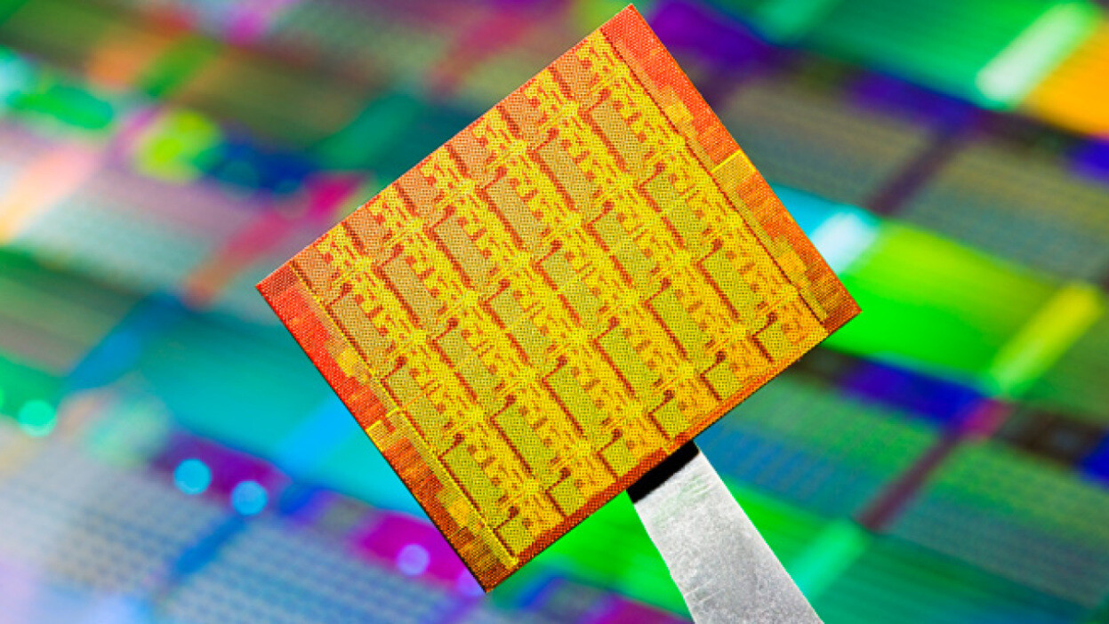
TSMC and Synopsys Bring Breakthrough NVIDIA Computational Lithography Platform to Production

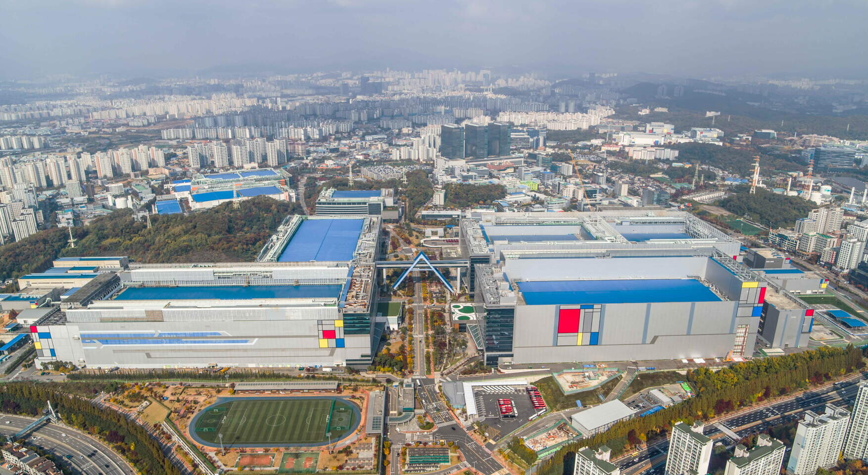
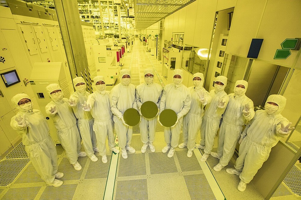
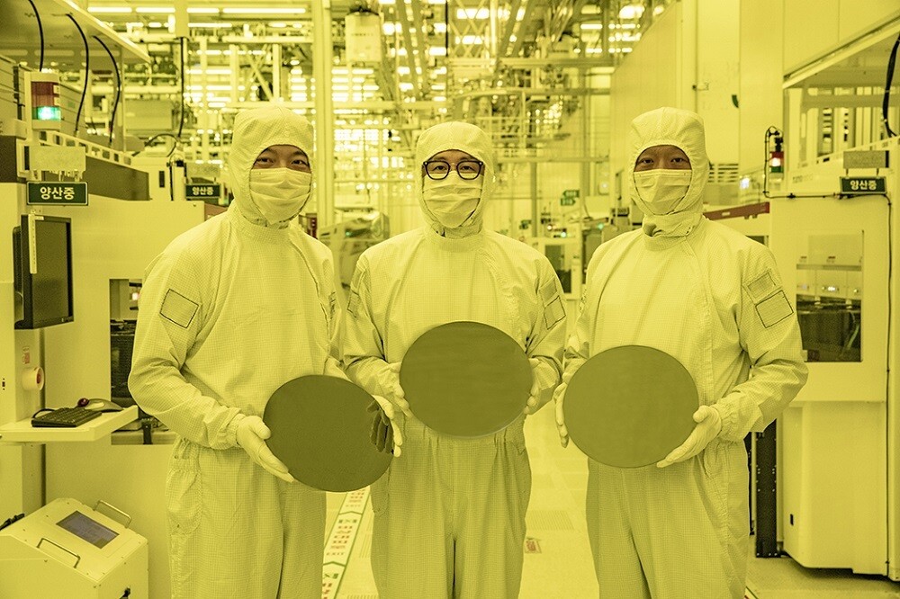
NVIDIA today announced that TSMC and Synopsys are going into production with NVIDIA's computational lithography platform to accelerate manufacturing and push the limits of physics for the next generation of advanced semiconductor chips. TSMC, the world's leading foundry, and Synopsys, the leader in silicon to systems design solutions, have integrated NVIDIA cuLitho with their software, manufacturing processes and systems to speed chip fabrication, and in the future support the latest-generation NVIDIA Blackwell architecture GPUs.

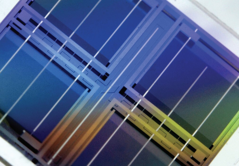
"Computational lithography is a cornerstone of chip manufacturing," said Jensen Huang, founder and CEO of NVIDIA. "Our work on cuLitho, in partnership with TSMC and Synopsys, applies accelerated computing and generative AI to open new frontiers for semiconductor scaling." NVIDIA also introduced new generative AI algorithms that enhance cuLitho, a library for GPU-accelerated computational lithography, dramatically improving the semiconductor manufacturing process over current CPU-based methods.

Intel Introduces Advisory Committee at Intel Foundry Direct Connect

During his keynote address today at Intel Foundry Direct Connect, Intel's inaugural foundry event, CEO Pat Gelsinger introduced four members of the company's Foundry Advisory Committee. The committee advises Intel on its IDM 2.0 strategy, including creation and development of a thriving systems foundry for the AI era.
The advisory committee includes leaders from the semiconductor industry and academia, two of whom are also members of Intel's board of directors:
  • Chi-Foon Chan, former Co-CEO of Synopsys; former Microprocessor Group general manager at NEC; director at PDF Solutions.
  • Joe Kaeser, former CEO of Siemens; supervisory board chair at Siemens Energy and Daimler Truck; supervisory board member at Linde; former member of the board of NXP semiconductor; member of the board of trustees at the World Economic Forum.
  • Tsu-Jae King Liu, vice chair of the Foundry Advisory Committee; dean of College of Engineering at the University of California, Berkeley; Intel director; and director at MaxLinear.
  • Lip-Bu Tan, chair of the Foundry Advisory Committee; former CEO of Cadence Design Systems; chairman of Walden International; and Intel director; director at Credo Technology Group and Schneider Electric.

Intel Announces Intel 14A (1.4 nm) and Intel 3T Foundry Nodes, Launches World's First Systems Foundry Designed for the AI Era

Intel Corp. today launched Intel Foundry as a more sustainable systems foundry business designed for the AI era and announced an expanded process roadmap designed to establish leadership into the latter part of this decade. The company also highlighted customer momentum and support from ecosystem partners - including Synopsys, Cadence, Siemens and Ansys - who outlined their readiness to accelerate Intel Foundry customers' chip designs with tools, design flows and IP portfolios validated for Intel's advanced packaging and Intel 18A process technologies.

The announcements were made at Intel's first foundry event, Intel Foundry Direct Connect, where the company gathered customers, ecosystem companies and leaders from across the industry. Among the participants and speakers were U.S. Secretary of Commerce Gina Raimondo, Arm CEO Rene Haas, Microsoft CEO Satya Nadella, OpenAI CEO Sam Altman and others.

Intel, Marvell, and Synopsys to Showcase Next-Gen Memory PHY IP Capable of 224 Gbps on 3nm-class FinFET Nodes

The sneak peeks from the upcoming IEEE Solid State Circuit Conference continues, as the agenda items unveil interesting tech that will be either unveiled or demonstrated there. Intel, Synopsys, and Marvell, are leading providers of DRAM physical layer interface (PHY) IP. Various processor, GPU, and SoC manufacturers license PHY and memory controller IP from these companies, to integrate with their designs. All three companies are ready with over 200 Gbps around the 2.69 to 3 petajoule per bit range. This energy cost is as important as the data-rate on offer; as it showcases the viability of the PHY for a specific application (for example, a smartphone SoC has to conduct its memory sub-system at a vastly more constrained energy budget compared to an HPC processor).

Intel is the first in the pack to showcase a 224 Gbps sub-picojoule/bit PHY transmitter that supports PAM4 and PAM6 signaling, and is designed for 3 nm-class FinFET foundry nodes. If you recall, Intel 3 will be the company's final FinFET node before it transitions to nanosheets with the Intel 20A node. At the physical layer, all digital memory signal is analogue, and Intel's IP focuses on the DAC aspect of the PHY. Next up, is a somewhat similar transceiver IP by Synopsys. This too claims 224 Gbps speeds at 3 pJ/b, but at a 40 dB insertion loss; and is designed for 3 nm class FinFET nodes such as the TSMC N3 family and Intel 3. Samsung's 3 nm node uses the incompatible GAAFET technology for its 3 nm EUV node. Lastly, there's Marvell, with a 212 Gb/s DSP-based transceiver for optical direct-detect applications on the 5 nm FinFET nodes, which is relevant for high speed network switching fabrics.

Synopsys to Acquire Ansys, Creating a Leader in Silicon to Systems Design Solutions

Synopsys (NASDAQ: SNPS) and Ansys (NASDAQ: ANSS) today announced that they have entered into a definitive agreement under which Synopsys will acquire Ansys. Under the terms of the agreement, Ansys shareholders will receive $197.00 in cash and 0.3450 shares of Synopsys common stock for each Ansys share, representing an enterprise value of approximately $35 billion based on the closing price of Synopsys common stock on December 21, 2023. Bringing together Synopsys' pioneering semiconductor electronic design automation (EDA) with Ansys' broad simulation and analysis portfolio will create a leader in silicon to systems design solutions.

"The megatrends of AI, silicon proliferation and software-defined systems are requiring more compute performance and efficiency in the face of growing, systemic complexity. Bringing together Synopsys' industry-leading EDA solutions with Ansys' world-class simulation and analysis capabilities will enable us to deliver a holistic, powerful and seamlessly integrated silicon to systems approach to innovation to help maximize the capabilities of technology R&D teams across a broad range of industries," said Sassine Ghazi, President and CEO of Synopsys. "This is the logical next step for our successful, seven-year partnership with Ansys and I look forward to working closely with Ajei and the talented Ansys team to realize the benefits of this combination for our customers, shareholders and employees."

Synopsys Expands Its ARC Processor IP Portfolio with New RISC-V Family

Synopsys, Inc. (Nasdaq: SNPS) today announced it has extended its ARC Processor IP portfolio to include new RISC-V ARC-V Processor IP, enabling customers to choose from a broad range of flexible, extensible processor options that deliver optimal power-performance efficiency for their target applications. Synopsys leveraged decades of processor IP and software development toolkit experience to develop the new ARC-V Processor IP that is built on the proven microarchitecture of Synopsys' existing ARC Processors, with the added benefit of the expanding RISC-V software ecosystem.

Synopsys ARC-V Processor IP includes high-performance, mid-range, and ultra-low power options, as well as functional safety versions, to address a broad range of application workloads. To accelerate software development, the Synopsys ARC-V Processor IP is supported by the robust and proven Synopsys MetaWare Development Toolkit that generates highly efficient code. In addition, the Synopsys.ai full-stack AI-driven EDA suite is co-optimized with ARC-V Processor IP to provide an out-of-the-box development and verification environment that helps boost productivity and quality-of-results for ARC-V-based SoCs.

Arm and Synopsys Strengthen Partnership to Accelerate Custom Silicon on Advanced Nodes

Synopsys today announced it has expanded its collaboration with Arm to provide optimized IP and EDA solutions for the newest Arm technology, including the Arm Neoverse V2 platform and Arm Neoverse Compute Subsystem (CSS). Synopsys has joined Arm Total Design where Synopsys will leverage their deep design expertise, the Synopsys.ai full-stack AI-driven EDA suite, and Synopsys Interface, Security, and Silicon Lifecycle Management IP to help mutual customers speed development of their Arm-based CSS solutions. The expanded partnership builds on three decades of collaboration to enable mutual customers to quickly develop specialized silicon at lower cost, with less risk and faster time to market.

"With Arm Total Design, our aim is to enable rapid innovation on Arm Neoverse CSS and engage critical ecosystem expertise at every stage of SoC development," said Mohamed Awad, senior vice president and general manager, Infrastructure Line of Business at Arm. "Our deep technical collaboration with Synopsys to deliver pre-integrated and validated IP and EDA tools will help our mutual customers address the industry's most complex computing challenges with specialized compute."

TSMC Announces Breakthrough Set to Redefine the Future of 3D IC

TSMC today announced the new 3Dblox 2.0 open standard and major achievements of its Open Innovation Platform (OIP) 3DFabric Alliance at the TSMC 2023 OIP Ecosystem Forum. The 3Dblox 2.0 features early 3D IC design capability that aims to significantly boost design efficiency, while the 3DFabric Alliance continues to drive memory, substrate, testing, manufacturing, and packaging integration. TSMC continues to push the envelope of 3D IC innovation, making its comprehensive 3D silicon stacking and advanced packaging technologies more accessible to every customer.

"As the industry shifted toward embracing 3D IC and system-level innovation, the need for industry-wide collaboration has become even more essential than it was when we launched OIP 15 years ago," said Dr. L.C. Lu, TSMC fellow and vice president of Design and Technology Platform. "As our sustained collaboration with OIP ecosystem partners continues to flourish, we're enabling customers to harness TSMC's leading process and 3DFabric technologies to reach an entirely new level of performance and power efficiency for the next-generation artificial intelligence (AI), high-performance computing (HPC), and mobile applications."

Synopsys and TSMC Streamline Multi-Die System Complexity with Unified Exploration-to-Signoff Platform and Proven UCIe IP on TSMC N3E Process

Synopsys, Inc. today announced it is extending its collaboration with TSMC to advance multi-die system designs with a comprehensive solution supporting the latest 3Dblox 2.0 standard and TSMC's 3DFabric technologies. The Synopsys Multi-Die System solution includes 3DIC Compiler, a unified exploration-to-signoff platform that delivers the highest levels of design efficiency for capacity and performance. In addition, Synopsys has achieved first-pass silicon success of its Universal Chiplet Interconnect Express (UCIe) IP on TSMC's leading N3E process for seamless die-to-die connectivity.

"TSMC has been working closely with Synopsys to deliver differentiated solutions that address designers' most complex challenges from early architecture to manufacturing," said Dan Kochpatcharin, head of the Design Infrastructure Management Division at TSMC. "Our long history of collaboration with Synopsys benefits our mutual customers with optimized solutions for performance and power efficiency to help them address multi-die system design requirements for high-performance computing, data center, and automotive applications."

Intel Foundry Services and Tower Semiconductor Announce New US Foundry Agreement

Intel Foundry Services (IFS) and Tower Semiconductor, a leading foundry for analog semiconductor solutions, today announced an agreement where Intel will provide foundry services and 300 mm manufacturing capacity to help Tower serve its customers globally. Under the agreement, Tower will utilize Intel's advanced manufacturing facility in New Mexico. Tower will invest up to $300 million to acquire and own equipment and other fixed assets to be installed in the New Mexico facility, providing a new capacity corridor of over 600,000 photo layers per month for Tower's future growth, enabling capacity to support forecasted customer demand for 300 mm advanced analog processing.

This agreement demonstrates the commitment from both Intel and Tower to expand their respective foundry footprints with unparalleled solutions and scaled capabilities. Intel will manufacture Tower's highly differentiated 65-nanometer power management BCD (bipolar-CMOS-DMOS) flows, among other flows at Intel's Fab 11X in Rio Rancho, New Mexico.

Arm Prepares for IPO: Apple, NVIDIA, Intel, and Samsung are Strategic Partners

Arm's impending IPO, valued between $60 billion and $70 billion, has reportedly garnered substantial backing from industry giants such as Apple, NVIDIA, Intel, and Samsung, as per sources cited in a Bloomberg report. This much-anticipated public offering serves as a litmus test for investor interest in new chip-related stocks and could reshape the tech industry landscape. While the information remains unofficial, it underscores the significant support Arm has received from major licensees, including Apple, AMD, Cadence, Intel, Google, NVIDIA, Samsung, and Synopsys, with each potentially contributing between $25 million and $100 million, a testament to their confidence in Arm's future prospects. Originally, SoftBank aimed to raise $8 billion to $10 billion through the IPO, but a strategic shift to retain a larger Arm stake revised the target to $5 billion to $7 billion.

This IPO's success holds paramount importance for SoftBank and its CEO, Masayoshi Son, particularly following the Vision Fund's substantial $30 billion loss in the previous fiscal year. Masayoshi Son is reportedly committed to maintaining significant control over Arm, planning to release no more than 10% of the company's shares during this initial phase, aligning with SoftBank's recent acquisition of the Vision Fund's Arm stake and reinforcing their belief in Arm's long-term potential. Arm has enlisted renowned global financial institutions such as Barclays, Goldman Sachs Group, JPMorgan Chase & Co., and Mizuho Financial Group to prepare for the IPO, highlighting the widespread interest in the offering and the anticipated benefits for these financial institutions.

Intel and Synopsys Expand Partnership to Enable Leading IP on Intel Advanced Process Nodes

Intel and Synopsys announced that they have entered into a definitive agreement to expand the companies' long-standing IP (intellectual property) and EDA (electronic design automation) strategic partnership with the development of a portfolio of IP on Intel 3 and Intel 18A for Intel's foundry customers. The availability of key IP on Intel advanced process nodes will create a more robust offering for new and existing Intel Foundry Services (IFS) customers.

"Marking another important step in our IDM 2.0 strategy, this transaction will foster a vibrant foundry ecosystem by allowing designers to fully realize the advantages of Intel 3 and Intel 18A process technologies and quickly bring differentiated products to market," said Stuart Pann, senior vice president and general manager of IFS. "Synopsys brings a strong track record of delivering high-quality IP to a broad customer base, and this agreement will help accelerate the availability of IP on advanced IFS nodes for mutual customers."

AMD CEO Lisa Su Notes: AI to Dominate Chip Design

Artificial intelligence (AI) has emerged as a transformative force in chip design, with recent examples from China and the United States showcasing its potential. Jensen Huang, CEO of Nvidia, believes that AI can empower individuals to become programmers, while Lisa Su, CEO of AMD, predicts an era where AI dominates chip design. During the 2023 World Artificial Intelligence Conference (WAIC) in Shanghai, Su emphasized the importance of interdisciplinary collaboration for the next generation of chip designers. To excel in this field, engineers must possess a holistic understanding of hardware, software, and algorithms, enabling them to create superior chip designs that meet system usage, customer deployment, and application requirements.

The integration of AI into chip design processes has gained momentum, fueled by the AI revolution catalyzed by large language models (LLMs). Both Huang and Mark Papermaster, CTO of AMD, acknowledge the benefits of AI in accelerating computation and facilitating chip design. AMD has already started leveraging AI in semiconductor design, testing, and verification, with plans to expand its use of generative AI in chip design applications. Companies are now actively exploring the fusion of AI technology with Electronic Design Automation (EDA) tools to streamline complex tasks and minimize manual intervention in chip design. Despite limited data and accuracy challenges, the "EDA+AI" approach holds great promise. For instance, Synopsys has invested significantly in AI tool research and recently launched Synopsys.ai, the industry's first end-to-end AI-driven EDA solution. This comprehensive solution empowers developers to harness AI at every stage of chip development, from system architecture and design to manufacturing, marking a significant leap forward in AI's integration into chip design workflows.

Synopsys and Samsung Collaborate to Deliver Broad IP Portfolio Across All Advanced Samsung Foundry Processes

Synopsys, Inc. today announced an expanded agreement with Samsung Foundry to develop a broad portfolio of IP to reduce design risk and accelerate silicon success for automotive, mobile, high-performance computing (HPC) and multi-die designs. This agreement expands Synopsys' collaboration with Samsung to enhance the Synopsys IP offering for Samsung's advanced 8LPU, SF5, SF4 and SF3 processes and includes Foundation IP, USB, PCI Express, 112G Ethernet, UCIe, LPDDR, DDR, MIPI and more. In addition, Synopsys will optimize IP for Samsung's SF5A and SF4A automotive process nodes to meet stringent Grade 1 or Grade 2 temperature and AEC-Q100 reliability requirements, enabling automotive chip designers to reduce their design effort and accelerate AEC-Q100 qualification. The auto-grade IP for ADAS SoCs will include design failure mode and effect analysis (DFMEA) reports that can save months of development effort for automotive SoC applications.

"Our extensive co-optimization efforts with Samsung across both EDA and IP help automotive, mobile, HPC, and multi-die system architects cope with the inherent challenges of designing chips for advanced process technologies," said John Koeter, senior vice president of product management and strategy for IP at Synopsys. "This extension of our decades-long collaboration provides designers with a low-risk path to achieving their design requirements and quickly launching differentiated products to the market."

Artificial Intelligence Helped Tape Out More than 200 Chips

In its recent Second Quarter of the Fiscal Year 2023 conference, Synopsys issued interesting information about the recent moves of chip developers and their usage of artificial intelligence. As the call notes, over 200+ chips have been taped out using Synopsys DSO.ai place-and-route (PnR) tool, making it a successful commercially proven AI chip design tool. The DSO.ai uses AI to optimize the placement and routing of the chip's transistors so that the layout is compact and efficient with regard to the strict timing constraints of the modern chip. According to Aart J. de Geus, CEO of Synopsys, "By the end of 2022, adoption, including 9 of the top 10 semiconductor vendors have moved forward at great speed with 100 AI-driven commercial tape-outs. Today, the tally is well over 200 and continues to increase at a very fast clip as the industry broadly adopts AI for design from Synopsys."

This is an interesting fact that means that customers are seeing the benefits of AI-assisted tools like DSO.ai. However, the company is not stopping there, and a whole suite of tools is getting an AI makeover. "We unveiled the industry's first full-stack AI-driven EDA suite, sydnopsys.ai," noted the CEO, adding that "Specifically, in parallel to second-generation advances in DSO.ai we announced VSO.ai, which stands for verification space optimization; and TSO.ai, test space optimization. In addition, we are extending AI across the design stack to include analog design and manufacturing." Synopsys' partners in this include NVIDIA, TSMC, MediaTek, Renesas, and IBM Research, all of which used AI-assisted tools for chip design efforts. A much wider range of industry players is expected to adopt these tools as chip design costs continue to soar as we scale the nodes down. With future 3 nm GPU costing an estimated $1.5 billion, 40% of that will account for software, and Synopsys plans to take a cut in that percentage.

Synopsys, TSMC and Ansys Strengthen Ecosystem Collaboration to Advance Multi-Die Systems

Accelerating the integration of heterogeneous dies to enable the next level of system scalability and functionality, Synopsys, Inc. (Nasdaq: SNPS) has strengthened its collaboration with TSMC and Ansys for multi-die system design and manufacturing. Synopsys provides the industry's most comprehensive EDA and IP solutions for multi-die systems on TSMC's advanced 7 nm, 5 nm and 3 nm process technologies with support for TSMC 3DFabric technologies and 3Dblox standard. The integration of Synopsys implementation and signoff solutions and Ansys multi-physics analysis technology on TSMC processes allows designers to tackle the biggest challenges of multi-die systems, from early exploration to architecture design with signoff power, signal and thermal integrity analysis.

"Multi-die systems provide a way forward to achieve reduced power and area and higher performance, opening the door to a new era of innovation at the system-level," said Dan Kochpatcharin, head of Design Infrastructure Management Division at TSMC. "Our long-standing collaboration with Open Innovation Platform (OIP) ecosystem partners like Synopsys and Ansys gives mutual customers a faster path to multi-die system success through a full spectrum of best-in-class EDA and IP solutions optimized for our most advanced technologies."

Huawei Reportedly Develops Chip Design Tools for 14 nm and Above

Amid the US sanctions, Chinese technology giant Huawei has reportedly developed tools to create processors with 14 nm and above lithography. According to Chinese media Yicai, Huawei and its semiconductor partners have teamed up to create replacement tools in place of US chip toolmakers like Cadence, Synopsys, and Mentor/Siemens. These three companies control all of the world's Electronic Design Automation (EDA) tools used for every step of chip design, from architecture to placement and routing to the final physical layout. Many steps need to be taken before making a tapeout of a physical chip, and Huawei's newly developed EDA tools will help the Chinese industry with US sanctions which crippled Huawei for a long time.

Having no access to US-made chipmaking tools, Huawei has invested substantial time into making these EDA tools. However, with competing EDA makers supporting lithography way below 14 nm, Huawei's job still needs to be completed. Chinese semiconductor factories are currently capable of 7 nm chip production, and Huawei itself is working on making a sub-7 nm EUV scanner to aid manufacturing goals and compete with the latest from TSMC and other. If Huawei can create EUV scanners that can achieve transistor sizes smaller than 7 nm, we expect to see their EDA tools keep pace as well. It is only a matter of time before they announce adaptation for smaller nodes.

NVIDIA, ASML, TSMC and Synopsys Set Foundation for Next-Generation Chip Manufacturing

NVIDIA today announced a breakthrough that brings accelerated computing to the field of computational lithography, enabling semiconductor leaders like ASML, TSMC and Synopsys to accelerate the design and manufacturing of next-generation chips, just as current production processes are nearing the limits of what physics makes possible.

The new NVIDIA cuLitho software library for computational lithography is being integrated by TSMC, the world's leading foundry, as well as electronic design automation leader Synopsys into their software, manufacturing processes and systems for the latest-generation NVIDIA Hopper architecture GPUs. Equipment maker ASML is working closely with NVIDIA on GPUs and cuLitho, and is planning to integrate support for GPUs into all of its computational lithography software products.

US Institutes GAA-FET Technology EDA Software Ban on China, Stalling sub-3nm Nodes

The US Government has instituted a ban on supply of GAA-FET EDA software to China (the Chinese government and companies in China). Humans can no longer design every single circuit on chips with tens of billions of transistors, and so EDA (electronics design automation) software is used to micromanage design based broadly on what chip architects want. Synopsys, Cadence, and Siemens are major EDA software suppliers. Intel is rumored to use an in-house EDA software that it doesn't sell, although this could change with the company roping in third-party foundries, such as TSMC, for cutting-edge logic chips (which will need the software to make sense of Intel's designs).

GAA or "gates-all-around" technology is vital to building transistors in the 3 nm and 2 nm silicon fabrication nodes. Samsung is already using GAA for its 3 nm node, while TSMC intends to use it with its 2N (2 nm) node. Intel is expected to use it with its Intel 20A (20 angstrom, or 2 nanometers) node. Both Intel and TSMC will debut nodes powered by GAAFETs for mass-production in 2024. The US Government has already banned the sales of EUV lithography machines to China, as well as machines fabricating 3D NAND flash chips with greater than 128 layers or 14 nm. In the past, technology embargoes have totally stopped China from copying or reverse-engineering western tech, or luring Taiwanese engineers armed with industry secrets away on the promise of wealth and a comfortable life in the Mainland.

Samsung Begins Chip Production Using 3nm Process Technology With GAA Architecture

Samsung Electronics, the world leader in semiconductor technology, today announced that it has started initial production of its 3-nanometer (nm) process node applying Gate-All-Around (GAA) transistor architecture. Multi-Bridge-Channel FET (MBCFET), Samsung's GAA technology implemented for the first time ever, defies the performance limitations of FinFET, improving power efficiency by reducing the supply voltage level, while also enhancing performance by increasing drive current capability. Samsung is starting the first application of the nanosheet transistor with semiconductor chips for high performance, low power computing application and plans to expand to mobile processors.

"Samsung has grown rapidly as we continue to demonstrate leadership in applying next-generation technologies to manufacturing, such as foundry industry's first High-K Metal Gate, FinFET, as well as EUV. We seek to continue this leadership with the world's first 3 nm process with the MBCFET," said Dr. Siyoung Choi, President and Head of Foundry Business at Samsung Electronics. "We will continue active innovation in competitive technology development and build processes that help expedite achieving maturity of technology."

Synopsys Introduces Industry's Highest Performance Neural Processor IP

Addressing increasing performance requirements for artificial intelligence (AI) systems on chip (SoCs), Synopsys, Inc. today announced its new neural processing unit (NPU) IP and toolchain that delivers the industry's highest performance and support for the latest, most complex neural network models. Synopsys DesignWare ARC NPX6 and NPX6FS NPU IP address the demands of real-time compute with ultra-low power consumption for AI applications. To accelerate application software development for the ARC NPX6 NPU IP, the new DesignWare ARC MetaWare MX Development Toolkit provides a comprehensive compilation environment with automatic neural network algorithm partitioning to maximize resource utilization.

"Based on our seamless experience integrating the Synopsys DesignWare ARC EV Processor IP into our successful NU4000 multi-core SoC, we have selected the new ARC NPX6 NPU IP to further strengthen the AI processing capabilities and efficiency of our products when executing the latest neural network models," said Dor Zepeniuk, CTO at Inuitive, a designer of powerful 3D and vision processors for advanced robotics, drones, augmented reality/virtual reality (AR/VR) devices and other edge AI and embedded vision applications. "In addition, the easy-to-use ARC MetaWare tools help us take maximum advantage of the processor hardware resources, ultimately helping us to meet our performance and time-to-market targets."

JEDEC Publishes HBM3 Update to High Bandwidth Memory (HBM) Standard

JEDEC Solid State Technology Association, the global leader in the development of standards for the microelectronics industry, today announced the publication of the next version of its High Bandwidth Memory (HBM) DRAM standard: JESD238 HBM3, available for download from the JEDEC website. HBM3 is an innovative approach to raising the data processing rate used in applications where higher bandwidth, lower power consumption and capacity per area are essential to a solution's market success, including graphics processing and high-performance computing and servers.

Synopsys Accelerates Multi-Die Designs with Industry's First Complete HBM3 IP and Verification Solutions

Synopsys, Inc. today announced the industry's first complete HBM3 IP solution, including controller, PHY, and verification IP for 2.5D multi-die package systems. HBM3 technology helps designers meet essential high-bandwidth and low-power memory requirements for system-on-chip (SoC) designs targeting high-performance computing, AI and graphics applications. Synopsys' DesignWare HBM3 Controller and PHY IP, built on silicon-proven HBM2E IP, leverage Synopsys' interposer expertise to provide a low-risk solution that enables high memory bandwidth at up to 921 GB/s.

The Synopsys verification solution, including Verification IP with built-in coverage and verification plans, off-the-shelf HBM3 memory models for ZeBu emulation, and HAPS prototyping system, accelerates verification from HBM3 IP to SoCs. To accelerate development of HBM3 system designs, Synopsys' 3DIC Compiler multi-die design platform provides a fully integrated architectural exploration, implementation and system-level analysis solution.

Intel Wins US Government Project to Develop Leading-Edge Foundry Ecosystem

The U.S. Department of Defense, through the NSTXL consortium-based S2MARTS OTA, has awarded Intel an agreement to provide commercial foundry services in the first phase of its multi-phase Rapid Assured Microelectronics Prototypes - Commercial (RAMP-C) program. The RAMP-C program was created to facilitate the use of a U.S.-based commercial semiconductor foundry ecosystem to fabricate the assured leading-edge custom and integrated circuits and commercial products required for critical Department of Defense systems. Intel Foundry Services, Intel's dedicated foundry business launched this year, will lead the work.

"One of the most profound lessons of the past year is the strategic importance of semiconductors, and the value to the United States of having a strong domestic semiconductor industry. Intel is the sole American company both designing and manufacturing logic semiconductors at the leading edge of technology. When we launched Intel Foundry Services earlier this year, we were excited to have the opportunity to make our capabilities available to a wider range of partners, including in the U.S. government, and it is great to see that potential being fulfilled through programs like RAMP-C." -Pat Gelsinger, Intel CEO.

Synopsys Launches Industry's First Complete IP Solution for PCI Express 6.0

Synopsys, Inc. today announced the industry's first complete IP solution for the PCI Express (PCIe ) 6.0 technology that includes controller, PHY and verification IP, enabling early development of PCIe 6.0 system-on-chip (SoC) designs. Built on Synopsys' widely deployed and silicon-proven DesignWare IP for PCIe 5.0, the new DesignWare IP for PCIe 6.0 supports the latest features in the standard specification including, 64 GT/s PAM-4 signaling, FLIT mode and L0p power state. Synopsys' complete IP solution addresses evolving latency, bandwidth and power-efficiency requirements of high-performance computing, AI and storage SoCs.

To achieve the lowest latency with maximum throughput for all transfer sizes, the DesignWare Controller for PCI Express 6.0 utilizes a MultiStream architecture, delivering up to 2X the performance of a single-stream design. The Controller, with available 1024-bit architecture, allows designers to achieve 64 GT/s x16 bandwidth while closing timing at 1 GHz. In addition, the controller provides optimal flow with multiple data sources and in multi-virtual channel implementations. To facilitate accelerated testbench development with built-in verification plan, sequences and functional coverage, the VC Verification IP for PCIe uses native SystemVerilog/UVM architecture that can be integrated, configured and customized with minimal effort.
Return to Keyword Browsing
Apr 30th, 2024 21:39 EDT change timezone

New Forum Posts

Popular Reviews

Controversial News Posts