News Posts matching #Technology

Return to Keyword Browsing

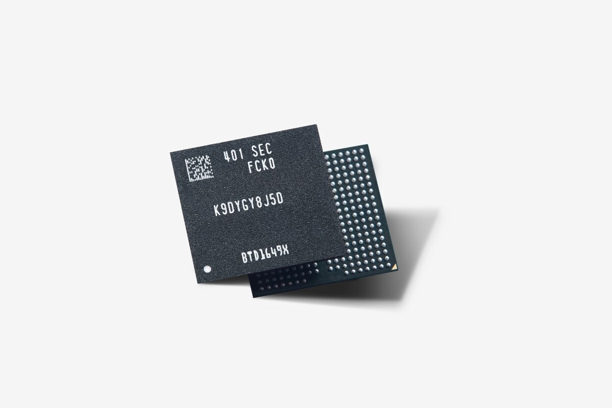
Micron to Receive US$6.1 Billion in CHIPS and Science Act Funding

Micron Technology, Inc., one of the world's largest semiconductor companies and the only U.S.-based manufacturer of memory, and the Biden-Harris Administration today announced that they have signed a non-binding Preliminary Memorandum of Terms (PMT) for $6.1 billion in funding under the CHIPS and Science Act to support planned leading-edge memory manufacturing in Idaho and New York.

The CHIPS and Science Act grants of $6.1 billion will support Micron's plans to invest approximately $50 billion in gross capex for U.S. domestic leading-edge memory manufacturing through 2030. These grants and additional state and local incentives will support the construction of one leading-edge memory manufacturing fab to be co-located with the company's existing leading-edge R&D facility in Boise, Idaho and the construction of two leading-edge memory fabs in Clay, New York.

TSMC Celebrates 30th North America Technology Symposium with Innovations Powering AI with Silicon Leadership

TSMC today unveiled its newest semiconductor process, advanced packaging, and 3D IC technologies for powering the next generation of AI innovations with silicon leadership at the Company's 2024 North America Technology Symposium. TSMC debuted the TSMC A16 technology, featuring leading nanosheet transistors with innovative backside power rail solution for production in 2026, bringing greatly improved logic density and performance. TSMC also introduced its System-on-Wafer (TSMC-SoW) technology, an innovative solution to bring revolutionary performance to the wafer level in addressing the future AI requirements for hyperscaler datacenters.

This year marks the 30th anniversary of TSMC's North America Technology Symposium, and more than 2,000 attended the event, growing from less than 100 attendees 30 years ago. The North America Technology Symposium in Santa Clara, California kicks off TSMC Technology Symposiums around the world in the coming months. The symposium also features an "Innovation Zone," designed to highlight the technology achievements of our emerging start-up customers.

Samsung Electronics Begins Industry's First Mass Production of 9th-Gen V-NAND

Samsung Electronics Co., Ltd., the world leader in advanced memory technology, today announced that it has begun mass production for its one-terabit (Tb) triple-level cell (TLC) 9th-generation vertical NAND (V-NAND), solidifying its leadership in the NAND flash market.

"We are excited to deliver the industry's first 9th-gen V-NAND, which will bring future applications leaps forward. In order to address the evolving needs for NAND flash solutions, Samsung has pushed the boundaries in cell architecture and operational scheme for our next-generation product," said SungHoi Hur, Head of Flash Product & Technology at Samsung Electronics. "Through our latest V-NAND, Samsung will continue to set the trend for the high-performance, high-density solid state drive (SSD) market that meets the needs for the coming AI generation."

Samsung and Qualcomm Achieve Innovative Industry-First Milestone With Advanced Modulation Technology

Samsung Electronics and Qualcomm Technologies, Inc. today announced that the companies successfully completed 1024 Quadrature Amplitude Modulation (QAM) tests for both Frequency Division Duplex (FDD) and Time Division Duplex (TDD) spectrum bands, marking an industry-first for FDD. This innovative milestone and collaboration demonstrate the companies' dedication to supporting operators increase 5G throughput and boost spectral efficiency of their networks.

QAM is an advanced modulation technology to transmit data or information more efficiently. This directly relates to how many bits of data can be delivered in each transmission. While 256 QAM is widely used in commercial networks, Samsung and Qualcomm Technologies recently accomplished the latest 1024 QAM defined in 3GPP Release 17 specifications. This enhanced QAM technology helps operators maximize their use of spectrum resources and allows mobile users to seamlessly enjoy various mobile services such as live video streaming and online multi-player gaming, which require higher download speeds.

Imagination's new Catapult CPU is Driving RISC-V Device Adoption

Imagination Technologies today unveils the next product in the Catapult CPU IP range, the Imagination APXM-6200 CPU: a RISC-V application processor with compelling performance density, seamless security and the artificial intelligence capabilities needed to support the compute and intuitive user experience needs for next generation consumer and industrial devices.

"The number of RISC-V based devices is skyrocketing with over 16Bn units forecast by 2030, and the consumer market is behind much of this growth" says Rich Wawrzyniak, Principal Analyst at SHD Group. "One fifth of all consumer devices will have a RISC-V based CPU by the end of this decade. Imagination is set to be a force in RISC-V with a strategy that prioritises quality and ease of adoption. Products like APXM-6200 are exactly what will help RISC-V achieve the promised success."

Introspect Technology Ships World's First GDDR7 Memory Test System

Introspect Technology, a JEDEC member and a leading manufacturer of test and measurement instruments, announced today that it has shipped the M5512 GDDR7 Memory Test System, the world's first commercial solution for testing JEDEC's newly minted JESD239 Graphics Double Data Rate (GDDR7) SGRAM specification. This category-creating solution enables graphics memory engineers, GPU design engineers, product engineers in both memory and GPU spaces, and system integrators to rapidly bring up new GDDR7 memory devices, debug protocol errors, characterize signal integrity, and perform detailed memory read/write functional stress testing without requiring any other tool.

The GDDR7 specification is the latest industry standard that is aimed at the creation of high-bandwidth and high-capacity memory implementations for graphics processing, artificial intelligence (AI), and AI-intensive networking. Featuring pulse-amplitude modulation (PAM) and an improved signal to noise ratio compared to other PAM4 standards used in networking, the GDDR7 PAM3 modulation technology achieves greater power-efficiency while significantly increasing data transmission bandwidth over constrained electrical channels.

Silicon Motion Unveils High-Performance Single Chip PCIe Gen4.0 BGA Ferri SSD with i-temp for Industrial and Automotive Applications

Silicon Motion Technology Corporation ("Silicon Motion"), a global leader in designing and marketing NAND flash controllers for solid-state storage devices, today introduced the new generation FerriSSD NVMe PCIe Gen 4 x4 BGA SSD. This latest solution features support for i-temp and integrates advanced IntelligentSeries technology, delivering robust data integrity in extreme temperature environments that meet the rigorous demands of industrial embedded systems and automotive applications.

The latest FerriSSD BGA SSD supports PCIe Gen 4 x4 and uses high density 3D NAND within a compact 16 mm x 20 mm BGA chip-scale package. With storage capacities up to 1 TB, these high-performance embedded SSDs utilize Silicon Motion's latest innovations to achieve high sequential read speeds exceeding 6 GB/s and sequential write speeds exceeding 4 GB/s. Equipped with Silicon Motion's proprietary IntelligentSeries data protection technology that enhances reliability and performance through the use of encryption, data caching, data scanning and protect features, as well as supporting the i-temp requirements of operating in extreme temperatures from -40°C to + 85°C. This latest FerriSSD offers a high performance and highly reliable embedded storage solution for a broad range of applications and operating environments including in-car computing, thin client computing, point-of-sale terminals, multifunction printers, telecommunications equipment, factory automation tools, and a wide range of server applications.

NVIDIA's Bryan Catanzaro Discusses Future of AI Personal Computing

Imagine a world where you can whisper your digital wishes into your device, and poof, it happens. That world may be coming sooner than you think. But if you're worried about AI doing your thinking for you, you might be waiting for a while. In a fireside chat Wednesday (March 20) at NVIDIA GTC, the global AI conference, Kanjun Qiu, CEO of Imbue, and Bryan Catanzaro, VP of applied deep learning research at NVIDIA, challenged many of the clichés that have long dominated conversations about AI. Launched in October 2022, Imbue made headlines with its Series B fundraiser last year, raising over $200 million at a $1 billion valuation.

The Future of Personal Computing
Qiu and Catanzaro discussed the role that virtual worlds will play in this, and how they could serve as interfaces for human-technology interaction. "I think it's pretty clear that AI is going to help build virtual worlds," said Catanzaro. "I think the maybe more controversial part is virtual worlds are going to be necessary for humans to interact with AI." People have an almost primal fear of being displaced, Catanzaro said, but what's much more likely is that our capabilities will be amplified as the technology fades into the background. Catanzaro compared it to the adoption of electricity. A century ago, people talked a lot about electricity. Now that it's ubiquitous, it's no longer the focus of broader conversations, even as it makes our day-to-day lives better.

Ubisoft Exploring Generative AI, Could Revolutionize NPC Narratives

Have you ever dreamed of having a real conversation with an NPC in a video game? Not just one gated within a dialogue tree of pre-determined answers, but an actual conversation, conducted through spontaneous action and reaction? Lately, a small R&D team at Ubisoft's Paris studio, in collaboration with Nvidia's Audio2Face application and Inworld's Large Language Model (LLM), have been experimenting with generative AI in an attempt to turn this dream into a reality. Their project, NEO NPC, uses GenAI to prod at the limits of how a player can interact with an NPC without breaking the authenticity of the situation they are in, or the character of the NPC itself.

Considering that word—authenticity—the project has had to be a hugely collaborative effort across artistic and scientific disciplines. Generative AI is a hot topic of conversation in the videogame industry, and Senior Vice President of Production Technology Guillemette Picard is keen to stress that the goal behind all genAI projects at Ubisoft is to bring value to the player; and that means continuing to focus on human creativity behind the scenes. "The way we worked on this project, is always with our players and our developers in mind," says Picard. "With the player in mind, we know that developers and their creativity must still drive our projects. Generative AI is only of value if it has value for them."

Arizona State University and Deca Technologies to Pioneer North America's First R&D Center for Advanced Fan-Out Wafer-Level Packaging

Arizona State University (ASU) and Deca Technologies (Deca), a premier provider of advanced wafer- and panel-level packaging technology, today announced a groundbreaking collaboration to create North America's first fan-out wafer-level packaging (FOWLP) research and development center.

The new Center for Advanced Wafer-Level Packaging Applications and Development is set to catalyze innovation in the United States, expanding domestic semiconductor manufacturing capabilities and driving advancements in cutting-edge fields such as artificial intelligence, machine learning, automotive electronics and high-performance computing.

EA Developers to Present Frostbite Engine Innovations at GDC 2024

San Francisco's annual Game Developers Conference (GDC) returns next week, bringing game devs together to share stories, experiences, and advice on everything from lighting scenes to writing resumes. Electronic Arts speakers will be participating in more than 25 in-person sessions this year, including multiple talks touching on innovative technologies driving the creation of next-gen games at EA.

This year's tech-focused sessions dig into the details of several successes, including Frostbite's non-interruptive expansion to new gaming platforms, SEED's work generating photorealistic facial rigs, and techniques for high-fidelity cloth simulation in Frostbite for EA SPORTS FC 24. There's also a fantastic talk from Respawn's Christopher Pierse and Samy Duc that explores the evolution of matchmaking techniques in Apex Legends, going all the way back to 2019.

Silicon Motion Unveils 6nm UFS 4.0 Controller for AI Smartphones, Edge Computing and Automotive Applications

Silicon Motion Technology Corporation ("Silicon Motion"), a global leader in designing and marketing NAND flash controllers for solid state storage devices, today introduced its UFS (Universal Flash Storage) 4.0 controller, the SM2756, as the flagship of the industry's broadest merchant portfolio of UFS controller solutions for the growing requirements of AI-powered smartphones as well as other high-performance applications including automotive and edge computing. The company also added a new, second generation SM2753 UFS 3.1 controller to broaden its portfolio of controllers now supporting UFS 4.0 to UFS 2.2 standards. Silicon Motion's UFS portfolio delivers high-performance and low power embedded storage for flagship to mainstream and value mobile and computing devices, supporting the broadest range of NAND flash, including next-generation high speed 3D TLC and QLC NAND.

The new SM2756 UFS 4.0 controller solution is the world's most advanced controller, built on leading 6 nm EUV technology and using MIPI M-PHY low-power architecture, providing the right balance of high performance and power efficiency to enable the all day computing needs of today's premium and AI mobile devices. The SM2756 achieves sequential read performance exceeding 4,300 MB/s and sequential write speeds of over 4,000 MB/s and supports the broadest range of 3D TLC and QLC NAND flash with densities of up to 2 TB.

Marvell Announces Industry's First 2 nm Platform for Accelerated Infrastructure Silicon

Marvell Technology, Inc., a leader in data infrastructure semiconductor solutions, is extending its collaboration with TSMC to develop the industry's first technology platform to produce 2 nm semiconductors optimized for accelerated infrastructure.

Behind the Marvell 2 nm platform is the company's industry-leading IP portfolio that covers the full spectrum of infrastructure requirements, including high-speed long-reach SerDes at speeds beyond 200 Gbps, processor subsystems, encryption engines, system-on-chip fabrics, chip-to-chip interconnects, and a variety of high-bandwidth physical layer interfaces for compute, memory, networking and storage architectures. These technologies will serve as the foundation for producing cloud-optimized custom compute accelerators, Ethernet switches, optical and copper interconnect digital signal processors, and other devices for powering AI clusters, cloud data centers and other accelerated infrastructure.

Sony Announces Layoff of 900 PlayStation Employees, London Studio Shuttered

Jim Ryan—President & CEO, Sony Interactive Entertainment—revealed a sobering restructuring plan earlier today: "The PlayStation community means everything to us, so I felt it was important to update you on a difficult day at our company. We have made the extremely hard decision to announce our plan to commence a reduction of our overall headcount globally by about 8% or about 900 people, subject to local law and consultation processes. Employees across the globe, including our studios, are impacted." Ryan's full email—addressed to the entire Sony Interactive Entertainment workforce—can be found here. It reveals that company leadership has decided to close its PlayStation London Studio—the South East UK team is/was reportedly working on an announced "PS5 online game." Microsoft revealed a larger scale layoff program late last month—affecting 1900 employees—albeit without shuttering any major development studios. A number of its California-based teams are in the process of ditching "traditional" office locations (including a former aircraft hangar), and are moving to a work from home (WFH) model.

The SIE chief believes that current circumstances are not sustainable: "These are incredibly talented people who have been part of our success, and we are very grateful for their contributions. However, the industry has changed immensely, and we need to future ready ourselves to set the business up for what lies ahead. We need to deliver on expectations from developers and gamers and continue to propel future technology in gaming, so we took a step back to ensure we are set up to continue bringing the best gaming experiences to the community." His email outlines an "impact for employees across all SIE regions—Americas, EMEA, Japan, and APAC," with reductions affecting native development teams and Firesprite, a Liverpool, UK-based studio (founded by former Psygnosis veterans). Hermen Hulst, Head of PlayStation Studios, also posted a blog entry on the subject of SIE global layoffs—he confirmed a number of reductions and project cancellations.

3D Nanoscale Petabit Capacity Optical Disk Format Proposed by Chinese R&D Teams

The University of Shanghai for Science and Technology (USST), Peking University and the Shanghai Institute of Optics and Fine Mechanics (SIOM) are collaborating on new Optical Data Storage (ODS) technologies—a recently published paper reveals that scientists are attempting to create 3D nanoscale optical disk memory that breaks into petabit capacities. Society (as a whole) has an ever-growing data demand—this requires the development of improved high-capacity storage technologies—the R&D teams believe that ODS presents a viable alternative route to traditional present day solutions: "data centers based on major storage technologies such as semiconductor flash devices and hard disk drives have high energy burdens, high operation costs and short lifespans."

The proposed ODS format could be a "promising solution for cost-effective long-term archival data storage." The researchers note that current (e.g Blu-ray) and previous generation ODS technologies have been: "limited by low capacities and the challenge of increasing areal density." In order to get ODS up to petabit capacity levels, several innovations are required—the Nature.com abstract stated: "extending the planar recording architecture to three dimensions with hundreds of layers, meanwhile breaking the optical diffraction limit barrier of the recorded spots. We develop an optical recording medium based on a photoresist film doped with aggregation-induced emission dye, which can be optically stimulated by femtosecond laser beams. This film is highly transparent and uniform, and the aggregation-induced emission phenomenon provides the storage mechanism. It can also be inhibited by another deactivating beam, resulting in a recording spot with a super-resolution scale." The novel optical storage medium relies on dye-doped photoresist (DDPR) with aggregation-induced emission luminogens (AIE-DDPR)—a 515 nm femtosecond Gaussian laser beam takes care of optical writing tasks, while a doughnut-shaped 639 nm continuous wave laser beam is tasked with retrieval. A 480 nm pulsed laser and a 592 nm continuous wave laser work in tandem to read data.

Cisco & NVIDIA Announce Easy to Deploy & Manage Secure AI Solutions for Enterprise

This week, Cisco and NVIDIA have announced plans to deliver AI infrastructure solutions for the data center that are easy to deploy and manage, enabling the massive computing power that enterprises need to succeed in the AI era. "AI is fundamentally changing how we work and live, and history has shown that a shift of this magnitude is going to require enterprises to rethink and re-architect their infrastructures," said Chuck Robbins, Chair and CEO, Cisco. "Strengthening our great partnership with NVIDIA is going to arm enterprises with the technology and the expertise they need to build, deploy, manage, and secure AI solutions at scale." Jensen Huang, founder and CEO of NVIDIA said: "Companies everywhere are racing to transform their businesses with generative AI. Working closely with Cisco, we're making it easier than ever for enterprises to obtain the infrastructure they need to benefit from AI, the most powerful technology force of our lifetime."

A Powerful Partnership
Cisco, with its industry-leading expertise in Ethernet networking and extensive partner ecosystem, together with NVIDIA, the inventor of the GPU that fueled the AI boom, share a vision and commitment to help customers navigate the transitions for AI with highly secure Ethernet-based infrastructure. Cisco and NVIDIA have offered a broad range of integrated product solutions over the past several years across Webex collaboration devices and data center compute environments to enable hybrid workforces with flexible workspaces, AI-powered meetings and virtual desktop infrastructure.

GIGABYTE Highlights its GPU Server Portfolio Ahead of World AI Festival

The World AI Cannes Festival (WAICF) is set to be the epicenter of artificial intelligence innovation, where the globe's top 200 decision-makers and AI innovators will converge for three days of intense discussions on groundbreaking AI strategies and use-cases. Against the backdrop of this premier event, GIGABYTE has strategically chosen to participate, unveiling its exponential growth in the AI and High-Performance Computing (HPC) market segments.

The AI industry has witnessed unprecedented growth, with Cloud Service Providers (CSP's) and data center operators spearheading supercomputing projects. GIGABYTE's decision to promote its GPU server portfolio with over 70+ models, at WAICF is a testament to the increasing demands from the French market for sovereign AI Cloud solutions. The spotlight will be on GIGABYTE's success stories on enabling GPU Cloud infrastructure, seamlessly powered by NVIDIA GPU technologies, as GIGABYTE aims to engage in meaningful conversations with end-users and firms dependent on GPU computing.

Nubis Communications and Alphawave Semi Showcase First Demonstration of Optical PCI Express 6.0 Technology

Nubis Communications, Inc., provider of low-latency high-density optical inter-connect (HDI/O), and Alphawave Semi (LN: AWE), a global leader in high-speed connectivity and compute silicon for the world's technology infrastructure, today announced their upcoming demonstration of PCI Express 6.0 technology driving over an optical link at 64GT/s per lane. Data Center providers are exploring the use of PCIe over Optics to greatly expand the reach and flexibility of the interconnect for memory, CPUs, GPUs, and custom silicon accelerators to enable more scalable and energy-efficient clusters for Artificial Intelligence and Machine Learning (ML/AI) architectures.

Nubis Communications and Alphawave Semi will be showing a live demonstration in the Tektronix booth at DesignCon, the leading conference for advanced chip, board, and system design technologies. An Alphawave Semi PCIe Subsystem with PiCORE Controller IP and PipeCORE PHY will directly drive and receive PCIe 6.0 traffic through a Nubis XT1600 linear optical engine to demonstrate a PCIe 6.0 optical link at 64GT/s per fiber, with optical output waveform measured on a Tektronix sampling scope with a high-speed optical probe.

Intel Foundry Services Get 18A Order: Arm-based 64-Core Neoverse SoC

Faraday Technology Corporation, a Taiwanese silicon IP designer, has announced plans to develop a new 64-core system-on-chip (SoC) utilizing Intel's most advanced 18A process technology. The Arm-based SoC will integrate Arm Neoverse compute subsystems (CSS) to deliver high performance and efficiency for data centers, infrastructure edge, and 5G networks. This collaboration brings together Faraday, Arm, and Intel Foundry Services. Faraday will leverage its ASIC design and IP solutions expertise to build the SoC. Arm will provide the Neoverse compute subsystem IP to enable scalable computing. Intel Foundry Services will manufacture the chip using its cutting-edge 18A process, which delivers one of the best-in-class transistor performance.

The new 64-core SoC will be a key component of Faraday's upcoming SoC evaluation platform. This platform aims to accelerate customer development of data center servers, high-performance computing ASICs, and custom SoCs. The platform will also incorporate interface IPs from the Arm Total Design ecosystem for complete implementation and verification. Both Arm and Intel Foundry Services expressed excitement about working with Faraday on this advanced Arm-based custom silicon project. "We're thrilled to see industry leaders like Faraday and Intel on the cutting edge of Arm-based custom silicon development," said an Arm spokesperson. Intel SVP Stuart Pann said, "We are pleased to work with Faraday in the development of the SoC based on Arm Neoverse CSS utilizing our most competitive Intel 18A process technology." The collaboration represents Faraday's strategic focus on leading-edge technologies to meet evolving application requirements. With its extensive silicon IP portfolio and design capabilities, Faraday wants to deliver innovative solutions and break into next-generation computing design.

Intel 15th-Generation Arrow Lake-S Could Abandon Hyper-Threading Technology

A leaked Intel documentation we reported on a few days ago covered the Arrow Lake-S platform and some implementation details. However, there was an interesting catch in the file. The leaked document indicates that the upcoming 15th-Generation Arrow Lake desktop CPUs could lack Hyper-Threading (HT) support. The technical memo lists Arrow Lake's expected eight performance cores without any threads enabled via SMT. This aligns with previous rumors of Hyper-Threading removal. Losing Hyper-Threading could significantly impact Arrow Lake's multi-threaded application performance versus its Raptor Lake predecessors. Estimates suggest HT provides a 10-15% speedup across heavily-threaded workloads by enabling logical cores. However, for gaming, disabling HT has negligible impact and can even boost FPS in some titles. So Arrow Lake may still hit Intel's rumored 30% gaming performance targets through architectural improvements alone.

However, a replacement for the traditional HT is likely to come in the form of Rentable Units. This new approach is a response to the adoption of a hybrid core architecture, which has seen an increase in applications leveraging low-power E-cores for enhanced performance and efficiency. Rentable Units are a more efficient pseudo-multi-threaded solution that splits the first thread of incoming instructions into two partitions, assigning them to different cores based on complexity. Rentable Units will use timers and counters to measure P/E core utilization and send parts of the thread to each core for processing. This inherently requires larger cache sizes, where Arrow Lake is rumored to have 3 MB of L2 cache per core. Arrow Lake is also noted to support faster DDR5-6400 memory. But between higher clocks, more E-cores, and various core architecture updates, raw throughput metrics may not change much without Hyper-Threading.

Jensen Huang's 2024 Prediction: "Every Industry Will Become a Technology Industry"

"This year, every industry will become a technology industry," NVIDIA founder and CEO Jensen Huang told attendees last Wednesday during the annual J.P. Morgan Healthcare Conference. "You can now recognize and learn the language of almost anything with structure, and you can translate it to anything with structure—so text-protein, protein-text," Huang said in a fireside chat with Martin Chavez, partner and vice chairman of global investment firm Sixth Street Partners and board chair of Recursion, a biopharmaceutical company. "This is the generative AI revolution."

The conversation, which took place at the historic San Francisco Mint, followed a presentation at the J.P. Morgan conference Monday by Kimberly Powell, NVIDIA's VP of healthcare. In her talk, Powell announced that Recursion is the first hosting partner to offer a foundation model through the NVIDIA BioNeMo cloud service, which is advancing into beta this month. She also said that Amgen, one of the first companies to employ BioNeMo, plans to advance drug discovery with generative AI and NVIDIA DGX SuperPOD—and that BioNeMo is used by a growing number of techbio companies, pharmas, AI software vendors and systems integrators. Among them are Deloitte, Innophore, Insilico Medicine, OneAngstrom, Recursion and Terray Therapeutics.

Formovie Makes a Splash at CES 2024 with Theatre and Gaming Laser TVs

Formovie Technology, Chinese maker of laser TV and smart projectors, unveiled its latest innovations at CES 2024 this week. The company showcased several new projectors leveraging cutting-edge laser technology to deliver new visual experiences. The star of the Formovie lineup was the new Formovie Theatre 4K Triple-Laser UST Projector. As the world's first 4K ultra-short throw projector with triple laser technology, it produces a staggeringly bright 2800 ANSI lumens image with 3000:1 contrast ration at a spectacular 150-inch scale. Viewers can expect true-to-life colors and infinite contrast thanks to Formovie's advanced laser light source. The company touts the product as the world's 1st Dolby Vision & Atmos UST projector, which also features ALLM and MEMC for smoother gaming. The sound system is a bespoke work by Bowers & Wilkins. A few booth demos were available to paint the picture of the technology.

In addition, Formovie introduced the slim and portable Formovie S5 projector. Weighing only 6.5 pounds, it's an ultra-compact model ideal for on-the-go use. The S5 still outputs a bright 1100 ANSI lumens image with smooth 4K quality enabled by ALPD laser technology. Rounding out the product showcase, Formovie displayed the award-winning Formovie V10 home theater projector. Recently honored with a CES 2023 Innovation Award, the V10 stands out for its 240 Hz refresh rate, 12 ms low latency, and 2500 ANSI lumens brightness—making it a top choice for gaming and movies.

Chinese Researchers Want to Make Wafer-Scale RISC-V Processors with up to 1,600 Cores

According to the report from a journal called Fundamental Research, researchers from the Institute of Computing Technology at the Chinese Academy of Sciences have developed a 256-core multi-chiplet processor called Zhejiang Big Chip, with plans to scale up to 1,600 cores by utilizing an entire wafer. As transistor density gains slow, alternatives like multi-chiplet architectures become crucial for continued performance growth. The Zhejiang chip combines 16 chiplets, each holding 16 RISC-V cores, interconnected via network-on-chip. This design can theoretically expand to 100 chiplets and 1,600 cores on an advanced 2.5D packaging interposer. While multi-chiplet is common today, using the whole wafer for one system would match Cerebras' breakthrough approach. Built on 22 nm process technology, the researchers cite exascale supercomputing as an ideal application for massively parallel multi-chiplet architectures.

Careful software optimization is required to balance workloads across the system hierarchy. Integrating near-memory processing and 3D stacking could further optimize efficiency. The paper explores lithography and packaging limits, proposing hierarchical chiplet systems as a flexible path to future computing scale. While yield and cooling challenges need further work, the 256-core foundation demonstrates the potential of modular designs as an alternative to monolithic integration. China's focus mirrors multiple initiatives from American giants like AMD and Intel for data center CPUs. But national semiconductor ambitions add urgency to prove domestically designed solutions can rival foreign innovation. Although performance details are unclear, the rapid progress shows promise in mastering modular chip integration. Combined with improving domestic nodes like the 7 nm one from SMIC, China could easily create a viable Exascale system in-house.

Intel Collaborates with Taiwanese OEMs to Develop Open IP Immersion Cooling Solution and Reference Design

Intel is expanding immersion cooling collaborations with Taiwanese partners to strengthen its data center offerings for AI workloads. This includes developing an industry-first open IP complete immersion cooling solution and reference design. Partners like Kenmec and Auras Technology will be key in implementing Intel's advanced cooling roadmap. Intel is also cooperating with Taiwan's Industrial Research Institute on a new lab for certifying high-performance computing cooling technologies to international standards. With local ecosystem partners, Intel aims to accelerate next-generation cooling solutions for Taiwanese and global data centers. Advanced cooling allows packing more performance into constrained data center footprints, which is critical for AI's rapid growth. Intel touts a superfluid-based modular cooling system achieving 1500 Watts+ heat dissipation for high-density deployments.

Meanwhile, Kenmec offers a range of liquid cooling products, from Coolant Distribution Units (CDU) to customized Open Rack version 3 (ORv3) water cooling cabinets, with solutions already Intel-certified. Intel wants to solidify its infrastructure leadership as AI workloads surge by fostering an open, collaborative ecosystem around optimized cooling technologies. While progressing cutting-edge immersion and liquid cooling hardware, cultivating shared validation frameworks and best practices ensures broad adoption. With AI-focused data centers demanding ever-greater density, power efficiency, and reliability, cooling can no longer be an afterthought. Intel's substantial investments in a robust cooling ecosystem highlight it as a priority right alongside silicon advances. By lifting up Taiwanese partners as strategic cooling co-innovators, Intel aims to cement future competitiveness.

Micron Technology, Inc. Reports Results for the First Quarter of Fiscal 2024

Micron Technology, Inc. (Nasdaq: MU) today announced results for its first quarter of fiscal 2024, which ended November 30, 2023.

Fiscal Q1 2024 highlights
  • Revenue of $4.73 billion versus $4.01 billion for the prior quarter and $4.09 billion for the same period last year
  • GAAP net loss of $1.23 billion, or $1.12 per diluted share
  • Non-GAAP net loss of $1.05 billion, or $0.95 per diluted share
  • Operating cash flow of $1.40 billion versus $249 million for the prior quarter and $943 million for the same period last year
"Micron's strong execution and pricing drove better-than-anticipated first quarter financial results," said Micron Technology President and CEO Sanjay Mehrotra. "We expect our business fundamentals to improve throughout 2024, with record industry TAM projected for calendar 2025. Our industry-leading High Bandwidth Memory for data center AI applications illustrates the strength of our technology and product roadmaps, and we are well positioned to capitalize on the immense opportunities artificial intelligence is fueling across end markets."
Return to Keyword Browsing
May 1st, 2024 01:38 EDT change timezone

New Forum Posts

Popular Reviews

Controversial News Posts