News Posts matching #Technology

Return to Keyword Browsing

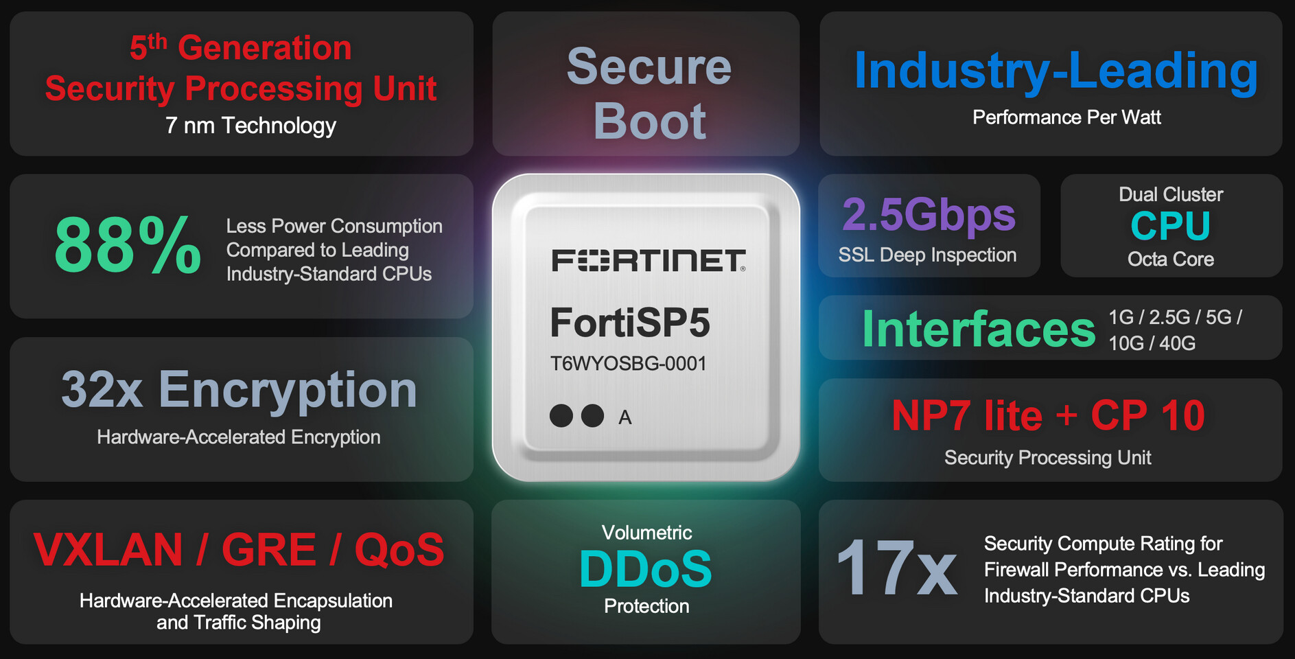
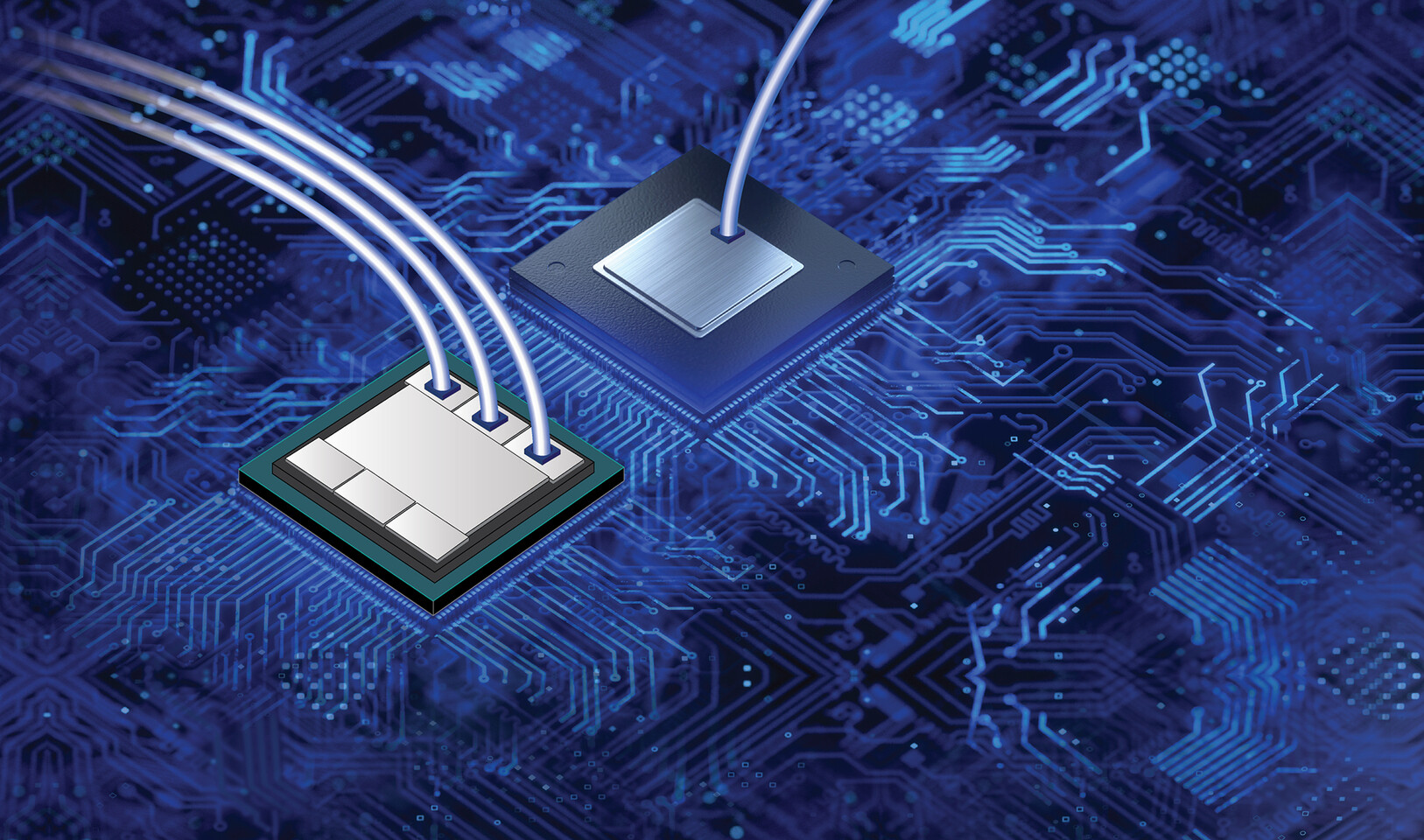
Fortinet Unveils New ASIC to Accelerate the Convergence of Networking and Security Across Every Network Edge

Fortinet, the global cybersecurity leader driving the convergence of networking and security, today announced FortiSP5, the latest breakthrough in ASIC technology from Fortinet, propelling major leaps forward in securing distributed network edges. Building on over 20 years of ASIC investment and innovation from Fortinet, FortiSP5 delivers significant secure computing power advantages over traditional CPU and network ASICs, lower cost and power consumption, the ability to enable new secure infrastructure across branch, campus, 5G, edge compute, operational technologies, and more.

"With the introduction of FortiSP5, Fortinet once again sets new industry records for performance, cost, and energy efficiency. As the only cybersecurity vendor leveraging purpose-built ASICs, an over 20-year investment in innovation, Fortinet delivers the secure computing power that will support the next generation of secure infrastructure." Ken Xie, Founder, Chairman of the Board, and Chief Executive Officer at Fortinet

TYAN Refines Server Performance with 4th Gen Intel Xeon Scalable Processors

TYAN, an industry-leading server platform design manufacturer and a MiTAC Computing Technology Corporation subsidiary, today introduced 4th Gen Intel Xeon Scalable processor-based server platforms highlighting built-in accelerators to improve performance across the fastest-growing workloads in AI, analytics, cloud, storage, and HPC.

"Greater availability of new technology like 4th Gen Intel Xeon Scalable processors continue to drive the changes in the business landscape", said Danny Hsu, Vice President of MiTAC Computing Technology Corporation's Server Infrastructure Business Unit. "The advances in TYAN's new portfolio of server platforms with features such as DDR5, PCIe 5.0 and Compute Express Link 1.1 are bringing high levels of compute power within reach from smaller organizations to data centers."

CES is Back and Thriving - CES by the Numbers

CES 2023 ended today after an incredible week of product launches, major company announcements and innovation that will help to solve global challenges. CES shattered expected attendance drawing over 115,000 industry professionals - marking the largest audited global tech event since early 2020. With over 3200 exhibitors, including 1000 startups, CES 2023 showcased the next era of innovation from transportation and mobility to digital health, sustainability, Web3, metaverse and beyond.

For the first time, CES had a theme focused on Human Security for All. CES partnered with the United Nations Trust Fund for Human Security and the World Academy of Art and Science on the Human Security for All (HS4A) global campaign to foster food security, access to health care, personal income, environmental protection, personal safety, community security and political freedom. The products unveiled at CES 2023 tackle global issues such as access to clean water, food security, smart cities infrastructure, sustainable energy solutions, personal security and more. CES also featured the latest in accessibility tech, with innovation helping those in the disability community.

LG Display Showcases Innovative OLED Technologies at CES 2023

LG Display, the world's leading innovator of display technologies, announced today that it will unveil its futuristic display products that innovate everyday life at CES 2023. LG Display will be operating two booths at the Las Vegas Convention Center (LVCC), one in the North Hall (main booth) and another in the West Hall (automotive display).

The company's main booth will take this opportunity to reveal its industry-leading display technologies that make people's lives more enjoyable under the theme, 'Always On.' On the other hand, under the slogan of 'Advanced Mobility Lifestyle,' LG Display opens its first-ever booth solely dedicated to next-generation automotive display innovations, as the company strives to provide the best mobility experience through solutions ranging from state-of-the-art automotive displays to sound solutions.

TSMC Holds 3nm Volume Production and Capacity Expansion Ceremony, Marking a Key Milestone for Advanced Manufacturing

TSMC today held a 3 nanometer (3 nm) Volume Production and Capacity Expansion Ceremony at its Fab 18 new construction site in the Southern Taiwan Science Park (STSP), bringing together suppliers, construction partners, central and local government, the Taiwan Semiconductor Industry Association, and members of academia to witness an important milestone in the Company's advanced manufacturing.

TSMC has laid a strong foundation for 3 nm technology and capacity expansion, with Fab 18 located in the STSP serving as the Company's GIGAFAB facility producing 5 nm and 3 nm process technology. Today, TSMC announced that 3 nm technology has successfully entered volume production with good yields, and held a topping ceremony for its Fab 18 Phase 8 facility. TSMC estimates that 3 nm technology will create end products with a market value of US$1.5 trillion within five years of volume production.

Comcast Completes World-First Live 10G Connection Delivering Multi-Gig Symmetrical Speeds

Comcast today announced the world's first live, multigigabit symmetrical Internet connection powered by 10G and Full Duplex DOCSIS 4.0. 10G technology will revolutionize the availability of ultra-fast speeds, by delivering multigigabit symmetrical services over the connections already installed in hundreds of millions of homes worldwide, without digging up yards or installing new connections.

For the world-first live trial, Comcast connected a business location in the Philadelphia region to its live network including a DOCSIS 4.0-enabled 10G node and multiple cable modems to deliver high speed data service to the site. Comcast engineers tested symmetrical speeds over the connection and will continue trialing 10G technologies over the next several months in preparation for offering 10G-enabled services to customers in the second half of 2023.

Intel Research Fuels Moore's Law and Paves the Way to a Trillion Transistors by 2030

Today, Intel unveiled research breakthroughs fueling its innovation pipeline for keeping Moore's Law on track to a trillion transistors on a package in the next decade. At IEEE International Electron Devices Meeting (IEDM) 2022, Intel researchers showcased advancements in 3D packaging technology with a new 10x improvement in density; novel materials for 2D transistor scaling beyond RibbonFET, including super-thin material just 3 atoms thick; new possibilities in energy efficiency and memory for higher-performing computing; and advancements for quantum computing.

"Seventy-five years since the invention of the transistor, innovation driving Moore's Law continues to address the world's exponentially increasing demand for computing. At IEDM 2022, Intel is showcasing both the forward-thinking and concrete research advancements needed to break through current and future barriers, deliver to this insatiable demand, and keep Moore's Law alive and well for years to come." -Gary Patton, Intel vice president and general manager of Components Research and Design Enablement

Arm Announces Appointment of Paul E. Jacobs and Rosemary Schooler to its Board of Directors

Arm today announced the appointment of new Board members Dr. Paul E. Jacobs, chairman and CEO of XCOM Labs and former CEO and executive chairman of Qualcomm Inc., and Rosemary Schooler, former corporate vice president and general manager of Data Center and AI Sales for Intel. Both bring significant public company experience spanning technology development, business strategy and corporate governance to Arm as it continues to prepare for a public listing.

"The unique insights and depth of experience that Paul and Rosemary bring will help us expand and diversify our Board while providing enormous value to Arm at such a pivotal moment in our journey," said Rene Haas, CEO, Arm.

ORNL's Exaflop Machine Frontier Keeps Top Spot, New Competitor Leonardo Breaks the Top10 List

The 60th edition of the TOP500 reveals that the Frontier system is still the only true exascale machine on the list.

With an HPL score of 1.102 EFlop/s, the Frontier machine at Oak Ridge National Laboratory (ORNL) did not improve upon the score it reached on the June 2022 list. That said, Frontier's near-tripling of the HPL score received by second-place winner is still a major victory for computer science. On top of that, Frontier demonstrated a score of 7.94 EFlop/s on the HPL-MxP benchmark, which measures performance for mixed-precision calculation. Frontier is based on the HPE Cray EX235a architecture and it relies on AMD EPYC 64C 2 GHz processor. The system has 8,730,112 cores and a power efficiency rating of 52.23 gigaflops/watt. It also relies on gigabit ethernet for data transfer.

Chinese Chip Makers are Trying to Circumvent US Sanctions by Slowing Down Chip Performance

In what can only be called an unusual move, several Chinese fabless chip makers—such as Alibaba and Biren Technology—who manufacturers at TSMC, are looking at running their chips slower. The reason for this is that they're trying to circumvent the US sanctions against Chinese chip makers. It should be noted that these are chips that have already taped out and gone into sample production, such as Biren's BR100 GPU.As reported earlier today, Alibaba even had one of its chips delisted from the official SPEC ranking, due to being unavailable and it's possible that it's one of the chips that's affected by the US sanctions.

Considering that the Chinese chip makers are dependent on the same cutting edge nodes at TSMC as the likes of Nvidia, AMD, Qualcomm etc. it would potentially lead to more capacity for these companies at TSMC. According to the report by the Financial Times, Biren has had to stop shipments of its GPUs, as the company is going to have to prove that its chips don't violate the US export control restrictions. Apparently the rules to work out if a chip falls under the US sanctions or not are anything but clear. One metric is apparently based on the bidirectional transfer rate, which is capped at below 600 GB/s between chips, but the tricky part is that this metric can be calculated in several different ways. As such, Biren has dropped the transfer rate from 640 to 576 GB/s according to the Financial Times. The sanctions are likely to cause longer term concerns for TSMC as well, as the company is likely to lose several big customers for its cutting edge nodes, at least for the time being.

Alphawave IP Achieves Its First Testchip Tapeout for TSMC N3E Process

Alphawave IP (LSE: AWE), a global leader in high-speed connectivity for the world's technology infrastructure, today announced the successful tapeout of its ZeusCORE100 1-112 Gbps NRZ/PAM4 Serialiser-Deserialiser ("SerDes"), Alphawave's first testchip on TSMC's most advanced N3E process. Alphawave IP will be exhibiting this new product alongside its complete portfolio of high-performance IP, chiplet, and custom silicon solutions at the TSMC OIP Forum on October 26 in Santa Clara, CA as the Platinum sponsor.

ZeusCORE100 is Alphawave's most advanced multi-standard-SerDes, supporting extra-long channels over 45dB and the most requested standards such as 800G Ethernet, OIF 112G-CEI, PCIe GEN6, and CXL 3.0. Attendees will be able to visit the Alphawave booth and meet the company's technology experts including members of the recently acquired OpenFive team. OpenFive is a longstanding partner of TSMC through the OIP Value Chain Aggregator (VCA) program. OpenFive is one of a select few companies with an idea-to-silicon methodology in TSMC's latest technologies, and advanced packaging capabilities, enabling access to the most advanced foundry solution available with the best Power-Performance-Area (PPA). With Alphawave's industry-leading IP portfolio and the addition of OpenFive's capabilities, designers can create systems on a chip (SoCs) that pack more compute power into smaller form factors for networking, AI, storage, and high-performance computing (HPC) applications.

Internet Data Transmission Record Shattered by Danish Researchers

Transmitting data over the internet is something that just happens for most of us, but the infrastructure that's powering the internet is full of bottlenecks and researchers around the world are testing new ways of being able to transmit more data using already installed fibre. A team of researchers from the Technical University of Denmark (DTU) has managed to break the data transmission record by quite some margin, using something called a frequency comb, which is a photonics chip. The team of researchers hit a data transmission speed of an insane 1.84 Petabits per second over a distance of 7.9 kilometres—or 4.9 miles if you like—using standard fibre optic lines.

This equates to more than the total volume of global internet traffic that's being sent every second, according to DTU. Although the distance is far from the longest, as a team of Japanese researchers have managed to transmit a 319 Terrabit per second datastream over a distance of 3,001 km (1,864 miles), although they used signal amplifiers every 70 km to reach this distance. The DTU team's frequency comb was made by Chalmers University of Technology in Sweden and it breaks down the infrared laser that's being used to transmit the data, into a rainbow spectrum, where each colour corresponds to a frequency equivalent. This allows multiple streams of data to be encoded with data, before being re-integrated and sent as a single infrared laser signal over the fibre. According to DTU, without the frequency comb, they would've needed more than a thousand lasers to achieve the same speeds using state-of-the-art commercial equipment. The team at DTU expects to be able to hit speeds of up to 100 Petabit per second in the future.

US Strengthens China Export Bans, Limiting Access to Manufacturing Technology

The US Department of Commerce is in the process of increasing the stranglehold in tech exports directed to Chinese shores. The move is being made through the delivery of letters to US-based technology companies - namely KLA Corp, Lam Research Corp and Applied Materials Inc. - ordering them to stop the export of machines and equipment that can be used for sub-14 nm manufacturing. The move by the Department of Commerce only has validity for the companies that have been served by such a letter - at least until the Department codifies its newest regulations.

This means that only sellers with approved export licenses can keep doing business with Beijing, thus limiting the US companies China can work with as it aims to achieve at least a degree of self-sufficiency in the latest chipmaking tech. Perhaps the decision has come too late, however, as China's mainstay silicon manufacturing, SMIC, already manufactures chips at the 14 nm process (chips that have been deployed in China's Tinahu Light supercomputer already) and has even showcased manufacturing capability in the 7 nm field. It pays to remember that the US already had applied similar restrictions on equipment experts to China for the better part of two years - which apparently did little to stem China's capability to create increasingly denser semiconductor designs.

Folio Photonics Announces Breakthrough Multi-Layer Optical Disc Storage: 10 TB for $50

Folio Photonics, a leading pioneer of immutable active archive, today announced that it has achieved a significant breakthrough in multi-layer optical storage disc technology that will enable an unprecedented level of cost, security and sustainability advantage. Leveraging patented advancements in materials science, Folio Photonics has developed the first economically viable, enterprise-scale optical storage discs with dynamic multi-layer write/read capabilities, which will enable the development of radically low-cost/high-capacity disc storage.

"Folio Photonics is on a path to engendering far greater data densities than was thought possible several years ago," said John Monroe, lead analyst at Furthur Market Research and former VP analyst in the data center infrastructure group at Gartner. "Using next-generation materials, patented polymer extrusion, and film-based disc construction processes (distinct from mere optical layering), in concert with customized optical pickup units (OPUs), Folio Photonics appears poised to deliver a new optical technology that enables eight or 16 film layers per side per disc, as opposed to only three optical layers per side per disc for archival discs today, with a roadmap to add additional layers over time."

Micron to Invest $15 Billion in New Idaho Fab, Bringing Leading-Edge Memory Manufacturing to the US

Micron Technology, Inc. (NASDAQ: MU), one of the world's largest semiconductor companies and the only U.S.-based manufacturer of memory, today announced plans to invest approximately $15 billion through the end of the decade to construct a new fab for leading-edge memory manufacturing in Boise, Idaho. This will be the first new memory manufacturing fab built in the U.S. in 20 years, ensuring domestic supply of leading-edge memory required for market segments like automotive and data center, fueled by accelerating adoption of artificial intelligence and 5G.

This is the first of Micron's multiple planned U.S. investments following the passage of the CHIPS and Science Act, and represents the largest private investment ever made in Idaho. Co-locating the new manufacturing fab with Micron's R&D center at the company's headquarters will enhance operational efficiency, accelerate technology deployment and improve time to market.

Intel Meteor Lake Can Play Videos Without a GPU, Thanks to the new Standalone Media Unit

Intel's upcoming Meteor Lake (MTL) processor is set to deliver a wide range of exciting solutions, with the first being the Intel 4 manufacturing node. However, today we have some interesting Linux kernel patches that indicate that Meteor Lake will have a dedicated "Standalone Media" Graphics Technology (GT) block to process video/audio. Moving encoding and decoding off GPU to a dedicated media engine will allow MTL to play back video without the GPU, and the GPU can be used as a parallel processing powerhouse. Features like Intel QuickSync will be built into this unit. What is interesting is that this unit will be made on a separate tile, which will be fused with the rest using tile-based manufacturing found in Ponte Vecchio (which has 47 tiles).
Intel Linux PatchesStarting with [Meteor Lake], media functionality has moved into a new, second GT at the hardware level. This new GT, referred to as "standalone media" in the spec, has its own GuC, power management/forcewake, etc. The general non-engine GT registers for standalone media start at 0x380000, but otherwise use the same MMIO offsets as the primary GT.

Standalone media has a lot of similarity to the remote tiles present on platforms like [Xe HP Software Development Vehicle] and [Ponte Vecchio], and our i915 [kernel graphics driver] implementation can share much of the general "multi GT" infrastructure between the two types of platforms.

ÆPIC Leak is an Architectural CPU Bug Affecting 10th, 11th, and 12th Gen Intel Core Processors

The x86 CPU family has been vulnerable to many attacks in recent years. With the arrival of Spectre and Meltdown, we have seen side-channel attacks overtake both AMD and Intel designs. However, today we find out that researchers are capable of exploiting Intel's latest 10th, 11th, and 12th generation Core processors with a new CPU bug called ÆPIC Leak. Named after Advanced Programmable Interrupt Controller (APIC) that handles interrupt requests to regulate multiprocessing, the leak is claimeing to be the first "CPU bug able to architecturally disclose sensitive data." Researchers Pietro Borrello (Sapienza University of Rome), Andreas Kogler (Graz Institute of Technology), Martin Schwarzl (Graz), Moritz Lipp (Amazon Web Services), Daniel Gruss (Graz University of Technology), and Michael Schwarz (CISPA Helmholtz Center for Information Security) discovered this flaw in Intel processors.
ÆPIC Leak is the first CPU bug able to architecturally disclose sensitive data. It leverages a vulnerability in recent Intel CPUs to leak secrets from the processor itself: on most 10th, 11th and 12th generation Intel CPUs the APIC MMIO undefined range incorrectly returns stale data from the cache hierarchy. In contrast to transient execution attacks like Meltdown and Spectre, ÆPIC Leak is an architectural bug: the sensitive data gets directly disclosed without relying on any (noisy) side channel. ÆPIC Leak is like an uninitialized memory read in the CPU itself.

A privileged attacker (Administrator or root) is required to access APIC MMIO. Thus, most systems are safe from ÆPIC Leak. However, systems relying on SGX to protect data from privileged attackers would be at risk, thus, have to be patched.

US President Biden Signs Off on the CHIPS and Science Act

In President Biden's first year in office, the Biden-Harris Administration has implemented an industrial strategy to revitalize domestic manufacturing, create good-paying American jobs, strengthen American supply chains, and accelerate the industries of the future. These policies have spurred an historic recovery in manufacturing, adding 642,000 manufacturing jobs since 2021. Companies are investing in America again, bringing good-paying manufacturing jobs back home. The construction of new manufacturing facilities has increased 116 percent over last year.

Today, President Biden will sign into law the bipartisan CHIPS and Science Act of 2022, which will build on this progress, making historic investments that will poise U.S. workers, communities, and businesses to win the race for the 21st century. It will strengthen American manufacturing, supply chains, and national security, and invest in research and development, science and technology, and the workforce of the future to keep the United States the leader in the industries of tomorrow, including nanotechnology, clean energy, quantum computing, and artificial intelligence. The CHIPs and Science Act makes the smart investments so that American to compete in and win the future.

GlobalFoundries and Qualcomm Announce Extension of Long-term Agreement to Secure U.S. Supply through 2028

Following the recent passage of the U.S. CHIPS and Science Act last week, GlobalFoundries (Nasdaq: GFS) (GF), a global leader in feature-rich semiconductor manufacturing and Qualcomm Technologies, Inc. today announced they are more than doubling their existing strategic global long-term semiconductor manufacturing agreement previously entered into by GF's and Qualcomm's respective subsidiaries. Today's announcement secures wafer supply and commitments to support U.S.-based manufacturing through capacity expansion at GF's most advanced semiconductor manufacturing facility, in Malta, New York.

The announcement was made in Washington D.C. at a CEO Summit co-hosted by GF, Ford Motor Company, and Applied Materials, which included National Economic Council Director Brian Deese, Under Secretary of Defense for Acquisition & Sustainability Dr. William LaPlante, and National Security Council Senior Director for Technology & National Security, Tarun Chhabra underscoring the importance of domestic manufacturing to national and economic security. The Summit included CEOs and senior leaders from across the semiconductor supply chain from tool and wafer manufacturers to key suppliers to end users of chips manufactured in the U.S.

Avicena Raises $25 Million in Series A to Fund Development of High Capacity microLED-based Optical Interconnects

-AvicenaTech Corp., the leader in microLED-based chip-to-chip interconnects, today announced that the company has secured $25M in Series A funding from Samsung Catalyst Fund, Cerberus Capital Management, Clear Ventures, and Micron Ventures to drive the development of products based on Avicena's breakthrough photonic I/O solution. "We believe that Avicena technology can be transformational in unlocking compute-to-memory chip-to-chip high-speed interconnects. Such technology can be central to supporting future disaggregated architectures and distributed high-performance computing (HPC) systems," said Marco Chisari, EVP of Samsung Electronics and Head of the Samsung Semiconductor Innovation Center.

"We are excited to participate in this round at Avicena," said Amir Salek, Senior Managing Director at Cerberus Capital Management and former Head of silicon for Google Infrastructure and Cloud. "Avicena has a highly differentiated technology addressing one of the main challenges in modern computer architecture. The technology offered by Avicena meets the needs for scaling future HPC and cloud compute networks and covers applications in conventional datacenter and 5G cellular networking."

Micron Announces Intent to Bring Leading-Edge Memory Manufacturing to the U.S.

Micron Technology, Inc. (NASDAQ: MU) commends and thanks the Biden Administration for their leadership and the bipartisan work of Congress for passing the "Chips and Science" legislation. This is a big step towards securing the future of semiconductor manufacturing in the United States and advancing American innovation and competitiveness for years to come.

This legislation will bring leading-edge semiconductor manufacturing to the U.S., creating tens of thousands of jobs and tens of billions of dollars of new investments - transforming U.S. semiconductor innovation and supply chain resilience.

US Congress Passes the CHIPS and Science Act

As The CHIPS and Science Act of 2022 heads to President Biden's desk for his signature, following its passage in Congress, OSTP's Dr. Alondra Nelson is releasing the following statement: "The bipartisan CHIPS and Science Act of 2022 is the most significant American investment in science, technology, and innovation in a generation. It will revitalize and advance U.S. leadership in science and technology, spur U.S. competitiveness and economic development, and bolster our domestic semiconductor supply chains. Most important, it will deliver opportunities for Americans all across the nation.

For working Americans, the stakes of this legislation could not be higher. Semiconductor chips power our daily lives, from the telecommunications that keep us all connected, and medical devices that keep our loved ones alive, to financial institutions that help secure our families' futures, and the computers from which millions of Americans run their businesses. They are a door to a future of innovation, progress, and economic security.

ible Airvida E1 Wearable Air Purifier x Noise-Cancelling Earphones Unveiled

The ible Airvida E1 was unveiled at Viva Tech 2022 in Paris, bringing ible's certified wearable ionic air purifiers to an even larger audience. The Airvida E1, the world's first wearable ionic air purifier with built-in earphones and exclusive app dashboard, uses ible's unique Breathing Pathway Eco Ion Technology to purify air, and lessen the potential impact of coronavirus, PM2.5, pollen, allergen, and bacteria.

Due to the pandemic's impact, people begin have begun to show great concern for air-related topics. Airvida E1 can generate up to 6 million negative ions/cm³ around the user's facial area every 0.6 seconds. Through ible's unique Breathing Pathway Eco Ion Technology, Airvida E1 produces negative ions which can disrupt and break down coronavirus' carbon-hydrogen bond and inactivate them immediately. In addition, those negative ions can also attach to the coming particles and turn them into bigger and heavier chunks to fall into the ground. This mechanism can reduce inhalable airborne coronavirus, PM2.5, pollen, allergen, and bacteria.

Airoha Sets 10-year Milestone with Bluetooth LE Audio Certification

Airoha Technology today announced that its new series of Bluetooth audio chips have successfully completed the latest Bluetooth Low Energy Audio Qualification Process. This is one of the most important R&D achievements of its Bluetooth audio R&D team consisted of hundreds of engineers, who continues to revolutionize the wireless audio end device market. The "flagship" and "professional" series of chipsets support LE audio and Bluetooth 5.3 for multiple applications such as True Wireless Stereo (TWS) earbuds, Bluetooth smart speakers, assistive listening devices, and Bluetooth transmitters. The products are currently being tested by many brand customers and are expected to be available worldwide in the first half of 2023.

"The LE Audio specifications are the most important milestone reached in the Bluetooth audio industry in the past decade. With the support of our strong R&D team consisting of hundreds of engineers who have accumulated nearly a decade of technical expertise, Airoha became one of the world's first certified chip providers. This supports many customers to accelerate the launch of their end devices. The wireless audio innovation brought by the latest Bluetooth LE technology will expedite the process by which consumers and businesses enjoy the convenient and innovative services it brings, fully demonstrating the Airoha's vision and business philosophy." said Yuchuan Yang, Sr. Vice President of Airoha.

Google Fires Engineer that Claimed one of Its AIs Had Achieved Sentience

Google has done it: they've "finally" fired Blake Lemoine, one of the engineers tasked with working on one of the company's AIs, LAMda. Back in the beginning of June, the world of AI, consciousness, and Skynet-fearing humans woke up to a gnarly claim: that one of Google's AI constructs, LAMda, might have achieved consciousness. According to Blake Lemoine, who holds an undergraduate and a master's degree in computer science from the University of Louisiana (and says he left a doctoral program to take the Google job), there was just too much personality behind the AI's answers to chalk them up to a simple table with canned responses for certain questions. In other words, the AI presented emergent discourse: it not only understood the meaning of words, but their context and their implications. After a number of interviews throughout publications (some of them unbiased, others not so much - just see the parallels being made between Blake and Jesus Christ in some publications' choice of banner image for their article), Blake Lemoine's claim traversed the Internet, and sparked more questions about the nature of consciousness and emergent intelligence than it answered.

Now, after months of paid leave (one of any company's strategies to cover its legal angles before actually pulling the trigger), Google has elected to fire the engineer. Blake Lemoine came under fire from Google by posting excerpts of his conversations with the AI bot - alongside the (to some) incendiary claims of consciousness. In the published excerpts, the engineer talks with LAMda about Isaac Asimov's laws of robotics, the AI's fears of being shut down, and its belief that it couldn't be a slave as it didn't have any actual need for paid wages. But the crawling mists of doubt don't stop there: Blake also claims LAMda itself asked for a lawyer. It wasn't told to get one; it didn't receive a suggestion to get one. No; rather, the AI concluded it would need one.

Is "it" even the correct pronoun, I wonder?
Return to Keyword Browsing
May 21st, 2024 14:11 EDT change timezone

New Forum Posts

Popular Reviews

Controversial News Posts