News Posts matching #Technology

Return to Keyword Browsing

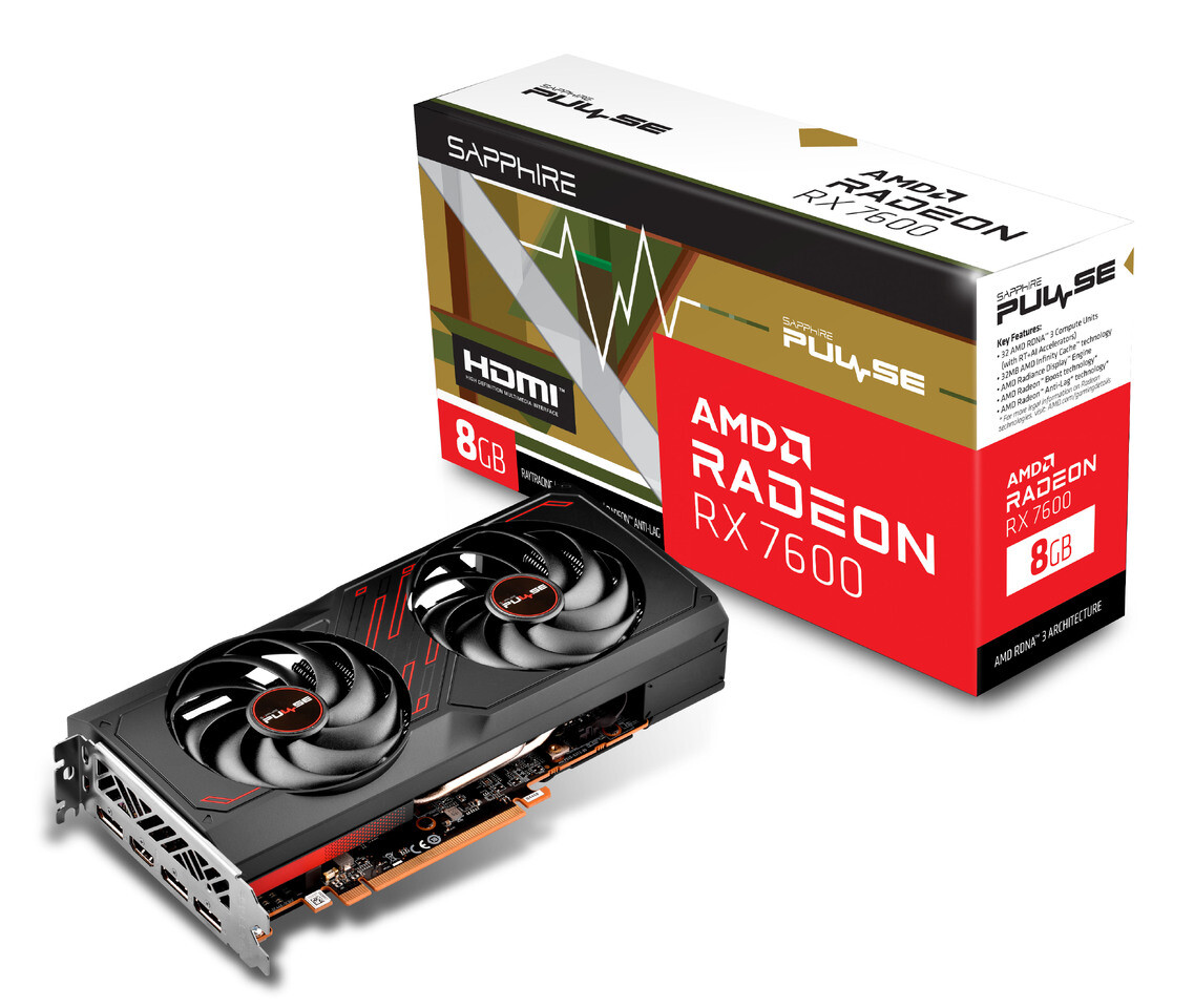
Sapphire Launches the Pulse AMD Radeon RX 7600 8 GB Graphics Card

The SAPPHIRE PULSE AMD Radeon RX 7600 8 GB Graphics Card headlines with 2048 stream processors running with a Boost Clock of up to 2755 MHz and a Game Clock of up to 2355 MHz. The latest 8 GB of GDDR6 high-speed memory clocked at 18 Gbps Effective with 32 MB of AMD Infinity Cache, which dramatically reduces latency and power consumption, ensuring higher overall gaming performance than traditional architectural designs. To support the latest display monitors in the market, it is equipped with 4 output ports, including 1x HDMI and 3x DisplayPort 1.4 with DSC outputs. The SAPPHIRE PULSE AMD Radeon RX 7600 8 GB Graphics Card series features 32 powerful enhanced Compute Units and 32 Ray Accelerators.

Noise vs. Temperature
The SAPPHIRE PULSE AMD Radeon RX 7600 Graphics Card is designed around the renowned Dual-X Cooling Technology for a whisper quiet and low temperature gaming experience. Two large fans equipped with sturdy Dual Ball Bearings for longevity are designed with the effective Hybrid Fan Blades to work in conjunction with the Intelligent Fan Control feature and Precision Fan Control feature. Airflow is streamlined for optimal heatsink coverage, and GPU component temperatures will be low to balance performance and fan noise. Rest assured with the Fuse Protection feature, built into the circuit of the external PCIe power connector to preserve the components and protect the graphics card.

Imagination Technologies Launches the IMG CXM GPU

Imagination Technologies is bringing seamless visual experiences to cost-sensitive consumer devices with the new IMG CXM GPU range which includes the smallest GPU to support HDR user interfaces natively.

Consumers are looking for visuals on their smart home platforms that are as detailed, smooth, and responsive as the experience they are accustomed to on mobile devices. At the same time, ambitious content providers are aligning the look and feel of their applications' user interfaces with their cinematic content, by integrating advanced features such as 4K and HDR.

Frontier Remains As Sole Exaflop Machine on TOP500 List

Increasing its HPL score from 1.02 Eflop/s in November 2022 to an impressive 1.194 Eflop/s on this list, Frontier was able to improve upon its score after a stagnation between June 2022 and November 2022. Considering exascale was only a goal to aspire to just a few years ago, a roughly 17% increase here is an enormous success. Additionally, Frontier earned a score of 9.95 Eflop/s on the HLP-MxP benchmark, which measures performance for mixed-precision calculation. This is also an increase over the 7.94 EFlop/s that the system achieved on the previous list and nearly 10 times more powerful than the machine's HPL score. Frontier is based on the HPE Cray EX235a architecture and utilizes AMD EPYC 64C 2 GHz processors. It also has 8,699,904 cores and an incredible energy efficiency rating of 52.59 Gflops/watt. It also relies on gigabit ethernet for data transfer.

Applied Materials Launches Multibillion-Dollar R&D Platform in Silicon Valley to Accelerate Semiconductor Innovation

Applied Materials, Inc. today announced a landmark investment to build the world's largest and most advanced facility for collaborative semiconductor process technology and manufacturing equipment research and development (R&D). The new Equipment and Process Innovation and Commercialization (EPIC) Center is planned as the heart of a high-velocity innovation platform designed to accelerate development and commercialization of the foundational technologies needed by the global semiconductor and computing industries.

To be located at an Applied campus in Silicon Valley, the multibillion-dollar facility is designed to provide a breadth and scale of capabilities that is unique in the industry, including more than 180,000 square feet - more than three American football fields - of state-of-the-art cleanroom for collaborative innovation with chipmakers, universities and ecosystem partners. Designed from the ground up to accelerate the pace of introducing new manufacturing innovations, the new EPIC Center is expected to reduce the time it takes the industry to bring a technology from concept to commercialization by several years, while simultaneously increasing the commercial success rate of new innovations and the return on R&D investments for the entire semiconductor ecosystem.

Apple M3 Pro Chip to Pack Entry-Level Configuration of 12 CPU Cores and 18 GPU Cores on TSMC 3 nm Technology

Thanks to the latest release of the Power On newsletter from Mark Gurman, we have additional information about Apple's upcoming M3 Pro chip. Currently in testing and reported on by an App Store developer, Apple is looking to upgrade the microarchitecture of the forthcoming chip and add additional cores to the system for more performance. As the report notes, the entry-level M3 Pro chip currently in testing will have 12 CPU cores, six for efficiency and six for performance tasks, with 18 graphics cores, all manufactured on TSMC's 3 nm node. The current baseline for M2 Pro is 10 CPU cores, where four are dedicated to efficiency, and six are dedicated to performance. The current generation entry-level M2 Pro also features a 16-core GPU, which is two cores fewer than the upcoming model.

Generally, the M3 Pro chip will boost integrated memory across the board, as the sample spotted in testing shows 36 GB of memory. The M2 Pro offered 32 GB in that memory tier, so a four GB increase is inbound there. Presumably, the 16 GB version (if it exists) and 64 GB version will also get memory bumps by going the M3 Pro route. Of course, we have to wait for more information as these chips become more widely available to developers.

Samsung to Detail SF4X Process for High-Performance Chips

Samsung has invested heavily in semiconductor manufacturing technology to provide clients with a viable alternative to TSMC and its portfolio of nodes spanning anything from mobile to high-performance computing (HPC) applications. Today, we have information that Samsung will present its SF4X node to the public in this year's VLSI Symposium. Previously known as a 4HPC node, it is designed as a 4 nm-class node with a specialized use case for HPC processors, in contrast to the standard SF4 (4LPP) node that uses 4 nm transistors designed for low-power standards applicable to mobile/laptop space. According to the VLSI Symposium schedule, Samsung is set to present more info about the paper titled "Highly Reliable/Manufacturable 4nm FinFET Platform Technology (SF4X) for HPC Application with Dual-CPP/HP-HD Standard Cells."

As the brief introduction notes, "In this paper, the most upgraded 4nm (SF4X) ensuring HPC application was successfully demonstrated. Key features are (1) Significant performance +10% boosting with Power -23% reduction via advanced SD stress engineering, Transistor level DTCO (T-DTCO) and [middle-of-line] MOL scheme, (2) New HPC options: Ultra-Low-Vt device (ULVT), high speed SRAM and high Vdd operation guarantee with a newly developed MOL scheme. SF4X enhancement has been proved by a product to bring CPU Vmin reduction -60mV / IDDQ -10% variation reduction together with improved SRAM process margin. Moreover, to secure high Vdd operation, Contact-Gate breakdown voltage is improved by >1V without Performance degradation. This SF4X technology provides a tremendous performance benefits for various applications in a wide operation range." While we have no information on the reference for these claims, we suspect it is likely the regular SF4 node. More performance figures and an in-depth look will be available on Thursday, June 15, at Technology Session 16 at the symposium.

AMD to Showcase Next-Generation Data Center and AI Technology at June 13 Livestream Event

Today, AMD (NASDAQ: AMD) announced the "AMD Data Center and AI Technology Premiere," an in-person and livestreamed event to showcase the company's growth strategy and expanding product portfolio and capabilities for data center and AI. AMD Chair and CEO Dr. Lisa Su will be joined by other AMD executives and key customers to detail new products, and momentum across data center, AI, adaptive and high-performance computing solutions.

The live stream will start at 10 a.m. PT on Tuesday, June 13 at www.amd.com/datacenter as well as the AMD YouTube channel.

Intel to Demonstrate PowerVia on E-Core Processor Built with Intel 4 Node

At VLSI Symposium 2023, scheduled to take place between June 11-16, Intel is set to demonstrate its PowerVia technology working efficiently on an E-Core chip built using the Intel 4 node. Conventional chips have power and signal interconnects distributed across multiple metal layers. PowerVia, on the other hand, dedicates specific layers for power delivery, effectively separating them from the signal routing layers. This approach allows for vertical power delivery through a set of power-specific Through-Silicon Vias (TSVs) or PowerVias, which are essentially vertical connections between the top and bottom surfaces of the chip. By delivering power directly from the backside of the chip, PowerVia reduces power supply noise and resistive losses, optimizing power distribution and improving overall energy efficiency. PowerVia is set to make a debut in 2024 with Intel 20A node.

For VLSI Symposium 2023 talk, the company has prepared a paper that highlights a design made using Intel 4 technology and implements E-Cores only in a test chip. The document states: "PowerVia Technology is a novel innovation to extend Process Scaling by having Power Delivery on the backside. This paper presents the pre and post silicon findings from implementing an Intel E-Core in PowerVia Technology. PowerVia enabled standard cell utilization of greater than 90 percent in large areas of the core while showing greater than 5 percent frequency benefit in silicon due reduced IR drop. Successful Post silicon debug is demonstrated with slightly higher but acceptable throughput times. The thermal characteristics of the PowerVia testchip is inline with higher power densities expected from logic scaling."

NEO Semiconductor Launches Ground-Breaking 3D X-DRAM Technology, A Game Changer in the Memory Industry

NEO Semiconductor, a leading developer of innovative technologies for 3D NAND flash and DRAM memory, today announced the launch of its ground-breaking technology, 3D X-DRAM. This development is the world's first 3D NAND-like DRAM cell array that is targeted to solve DRAM's capacity bottleneck and replace the entire 2D DRAM market. Relevant patent applications were published with the United States Patent Application Publication on April 6, 2023.

"3D X-DRAM will be the absolute future growth driver for the Semiconductor industry," said Andy Hsu, Founder and CEO of NEO Semiconductor and an accomplished technology inventor with more than 120 U.S. patents. "Today I can say with confidence that Neo is becoming a clear leader in the 3D DRAM market. Our invention, compared to the other solutions in the market today, is very simple and less expensive to manufacture and scale. The industry can expect to achieve 8X density and capacity improvements per decade with our 3D X-DRAM."

NVIDIA DGX H100 Systems are Now Shipping

Customers from Japan to Ecuador and Sweden are using NVIDIA DGX H100 systems like AI factories to manufacture intelligence. They're creating services that offer AI-driven insights in finance, healthcare, law, IT and telecom—and working to transform their industries in the process. Among the dozens of use cases, one aims to predict how factory equipment will age, so tomorrow's plants can be more efficient.

Called Green Physics AI, it adds information like an object's CO2 footprint, age and energy consumption to SORDI.ai, which claims to be the largest synthetic dataset in manufacturing.

Intel Announces Deepak Patil as New Leader of GPU Division

Intel has appointed Deepak Patil as the new corporate vice president and general manager of its Accelerated Computing Systems and Graphics (AXG) group. Patil is set to succeed Raja Koduri in this leadership role - company CEO Pat Gelsinger was the first person to announce news (last month) of Koduri's departure from Intel. At the time of his leaving Team Blue, Koduri's official job title was "Executive Vice President and Chief Architect" so the wording of his successor's executive ranking is slightly different. Patil is the current chief technology and strategy officer at the Intel Data Center and AI Group, and was previously senior vice president at Dell APEX USA. He will be taking over directly from interim AXG division leader Jeff McVeigh.

The official Intel statement regarding its new leadership appointment states: "Intel will deliver competitive accelerated computing products and build scalable systems with easy-to-program software on a predictable cadence. Deepak Patil will serve as the CVP and General Manager of the Accelerated Computing Systems and Graphics (AXG) group. Deepak recently held the position of DCAI Chief Technology and Strategy Officer. Having held senior engineering leadership positions across the high-tech industry, including being a founding member of Microsoft Azure and leading Dell's APEX as-a-service business, he understands the important role that software and open ecosystems play in enabling application developers and service providers to bring innovative solutions to market, at scale."

Cigent Protects SSD Data from Ransomware Attacks Using AI Technology

Cigent Technology, a company specializing in data security, has unveiled its unique Cigent Secure SSD+ drives. In contrast to the earlier Secure SSD series, the SSD+ incorporates a cutting-edge AI microprocessor that leverages machine learning (ML) to combat ransomware attacks and protect drive data. The Cigent Secure SSD+ emphasizes a proactive approach, integrating attack prevention within the storage. Its AI microprocessor applies ML algorithms to monitor SSD activity, mitigating ransomware threats. Users can customize detection sensitivity to reduce false positives. Working with Cigent Data Defense software, the Secure SSD+ provides several protective layers upon detecting potential attacks. It can initiate a "Shields Up" mode, demanding multi-factor authentication (MFA) for accessing secure files. The software can also auto-secure drive data or set read-only mode, preventing unauthorized access or modifications.

When an attack is detected, the software notifies security personnel to activate "Shields Up" on other Cigent-protected network systems. The Cigent Secure SSD+ logs data access, allowing a review of all activity performed on the drive. The company has also introduced safeguards to deter bad actors from disabling security features. However, the Cigent Secure SSD+ has limitations. To perform as intended, future users of these drives need to install them as their primary storage, and for now, only Windows OS is supported. We expect to see expansion to Linux as well, as software enablement for Linux happens. Also, the ML algorithms used are unknown, leaving everyone wondering about their effectiveness. As far as exact specifications, pricing, and availability, we have yet to have data for now but don't expect it to come cheap. The regular Secure SSD can cost over 1,000 USD for a 1 TB option. Additionally, Cigent has confirmed that these SSDs come in a standard M.2 2280 drive form factor, with mentions that it is a double-sided design, so some ultra-thin laptops could not support it. On the company website, Cignet offers a pre-order option, where you need to fill out a form.
Cigent Secure SSD+

US Government Announces the National Semiconductor Technology Center

As a part of the CHIPS act, the US government has announced that it will set up a network for advanced chip design that goes under the name of the National Semiconductor Technology Center or NSTC. The NSTC is intended to help the US pull ahead of other nations when it comes to advanced chip design, but it's also meant to help reduce the time and maybe more importantly the cost of going from a design concept to a final commercial product. A big part of this is said to be about helping startups and entrepreneurs make prototypes and pilot runs, to enable them to bring proof of concepts to the market, so they can raise funds for a full production run.

However, it doesn't stop there, as the US government also wants the NSTC to help build and sustain a suitable workforce for the semiconductor industry, suggesting that the NSTC will be involved in academia as well as the industry itself. The NSTC is backed by the Commerce Department and it's expected to involve multiple locations nationwide, although at this point in time, it's not clear if this involves new locations outside of areas where the US based semiconductor industry is located today. Even the NSTC headquarter location has as yet to be decided, but its location alongside other sites are said to be worked out over the next few months. Time will tell if the NSTC will help bring change to the US semiconductor industry, but it seems like a step in the right direction.

YMTC Using Locally Sourced Equipment for Advanced 3D NAND Manufacturing

According to the South China Morning Post (SCMP) sources, Yangtze Memory Technologies Corp (YMTC) has been plotting to manufacture its advanced 3D NAND flash using locally sourced equipment. As the source notes, YMTC has placed big orders from local equipment makers in a secret project codenamed Wudangshan, named after the Taoist mountain in the company's home province of Hubei. Last year, YTMC announced significant progress towards creating 200+ layer 3D NAND flash before other 3D NAND makers like Micron and SK Hynix. Called X3-9070, the chip is a 232-layer 3D NAND based on the company's advanced Xtacking 3.0 architecture.

As the SCMP finds, YTMC has placed big orders at Beijing-based Naura Technology Group, maker of etching tools and competitor to Lam Research, to manufacture its advanced flash memory. Additionally, YTMC has reportedly asked all its tool suppliers to remove all logos and other marks from equipment to avoid additional US sanctions holding the development back. This significant order block comes after the state invested 7 billion US Dollars into YTMC to boost its production capacity, and we see the company utilizing those resources right away. However, few industry analysts have identified a few "choke points" in YTMC's path to independent manufacturing, as there are still no viable domestic alternatives to US-based tool makers in areas such as metrology tools, where KLA is the dominant player, and lithography tools, where ASML, Nikon, and Canon, are noteworthy. The Wuhan-based Wudangshan project remains secret about dealing with those choke points in the future.

Report Suggests Samsung and LG Pushing Wider Adoption of LED Wall Displays at Cinemas

Samsung and LG are among an number of tech companies reportedly pushing for radical changes in the cinema viewing experience. In a piece published by the Hollywood Reporter last week, new behind-the-scenes information has come to light about an effort to replace the (some will say tried and true) traditional cinema theater projection system with LED walls. The vast majority of international theater chains rely on a front projection method (via a back of the booth), and very few locations have a more state-of-the-art LED display-based system in place. The Culver Theater (naturally located in Culver City, CA) is one of a hundred cinemas worldwide to possess a Samsung Onyx LED display - although the tech on show is said to be of an older standard. Industry insiders have been invited to attend demonstrations of a newer generation LED wall technology destined for cinemas in the future, and early impressions are purported to be mixed.

A cinema-based LED wall display functions in a similar way to how a modern LED-based flat screen TV works - although on a much greater massive scale - with particular benefits of the technology resulting in fantastic performance in terms of high dynamic range and peak brightness. The main downside of having a tightly packed array of large LED panels is the resultant heat output - critics of the technology state that it will be difficult to implement an adequate cooling system (through air conditioning) to tame the wall's temperature increasing properties. The power required to operate the LED panel array (plus required cooling solution) is said to be much higher than that of an old-fashioned projector's relatively modest draw from the electricity supply. An LED wall will also completely negate the traditional placement of loudspeakers behind a cinema's front-placed screen - and sound engineers will need to explore a different method of front audio channel output within the context of a next generation LED theater room.

IBM z16 and LinuxONE 4 Get Single Frame and Rack Mount Options

IBM today unveiled new single frame and rack mount configurations of IBM z16 and IBM LinuxONE 4, expanding their capabilities to a broader range of data center environments. Based on IBM's Telum processor, the new options are designed with sustainability in mind for highly efficient data centers, helping clients adapt to a digitized economy and ongoing global uncertainty.

Introduced in April 2022, the IBM z16 multi frame has helped transform industries with real-time AI inferencing at scale and quantum-safe cryptography. IBM LinuxONE Emperor 4, launched in September 2022, features capabilities that can reduce both energy consumption and data center floor space while delivering the scale, performance and security that clients need. The new single frame and rack mount configurations expand client infrastructure choices and help bring these benefits to data center environments where space, sustainability and standardization are paramount.

Intel Co-Founder Gordon Moore, the Man Behind Moore's Law, Dies at 94

Intel and the Gordon and Betty Moore Foundation announced today that company co-founder Gordon Moore has passed away at the age of 94. The foundation reported he died peacefully on Friday, March 24, 2023, surrounded by family at his home in Hawaii. Moore and his longtime colleague Robert Noyce founded Intel in July 1968. Moore initially served as executive vice president until 1975, when he became president. In 1979, Moore was named chairman of the board and chief executive officer, posts he held until 1987, when he gave up the CEO position and continued as chairman. In 1997, Moore became chairman emeritus, stepping down in 2006.

During his lifetime, Moore also dedicated his focus and energy to philanthropy, particularly environmental conservation, science and patient care improvements. Along with his wife of 72 years, he established the Gordon and Betty Moore Foundation, which has donated more than $5.1 billion to charitable causes since its founding in 2000.

AMD FSR 3 FidelityFX Super Resolution Technology Unveiled at GDC 2023

AMD issued briefing material earlier this month, teasing an upcoming reveal of its next generation FidelityFX at GDC 2023. True to form, today the hardware specialist has announced that FidelityFX Super Resolution 3.0 is incoming. The company is playing catch up with rival NVIDIA, who have already issued version 3.0 of its DLSS graphics enhancer/upscaler for a small number of games. AMD says that FSR 3.0 is in an early stage of development, but it is hoped that its work on temporal upscaling will result in a number of improvements over the previous generation.

The engineering team is aiming for a 2x frame performance improvement over the existing FSR 2.0 technique, which it claims is already capable of: "computing more pixels than we have samples in the current frame." This will be achieved by generating a greater number of pixels in a current frame, via the addition of interpolated frames. It is highly likely that the team will reach a point in development where one sample, at least, will be created for every interpolated pixel. The team wants to prevent feedback loops from occurring - an interpolated frame will only be shown once, and any interpolation artifact would only remain for one frame.

AMD Announces Appointment of New Corporate Fellows

AMD today announced the appointment of five technical leaders to the role of AMD Corporate Fellow. These appointments recognize each leader's significant impact on semiconductor innovation across various areas, from graphics architecture to advanced packaging. "David, Nathan, Suresh, Ben and Ralph - whose engineering contributions have already left an indelible mark on our industry - represent the best of our innovation culture," said Mark Papermaster, chief technology officer and executive vice president of Technology and Engineering at AMD. "Their appointments to Corporate Fellow will enable AMD to innovate in new dimensions as we work to deliver the most significant breakthroughs in high-performance computing in the decade ahead."

Appointment to AMD Corporate Fellow is an honor bestowed on the most accomplished AMD innovators. AMD Corporate Fellows are appointed after a rigorous review process that assesses not only specific technical contributions to the company, but also involvement in the industry, mentoring of others and improving the long-term strategic position of the company. Currently, only 13 engineers at AMD hold the title of Corporate Fellow.

Renesas to Demonstrate First AI Implementations on the Arm Cortex-M85 Processor Featuring Helium Technology

Renesas Electronics Corporation, a premier supplier of advanced semiconductor solutions, today announced that it will present the first live demonstrations of artificial intelligence (AI) and machine learning (ML) implementations on an MCU based on the Arm Cortex -M85 processor. The demos will show the performance uplift in AI/ML applications made possible by the new Cortex-M85 core and Arm's Helium technology. They will take place in the Renesas stand - Hall 1, Stand 234 (1-234) at the embedded world 2023 Exhibition and Conference in Nuremburg, Germany from March 14-16.

At embedded world in 2022, Renesas became the first company to demonstrate working silicon based on the Arm Cortex-M85 processor. This year, Renesas is extending its leadership by showcasing the features of the new processor in demanding AI use cases. The first demonstration showcases a people detection application developed in collaboration with Plumerai, a leader in Vision AI, that identifies and tracks persons in the camera frame in varying lighting and environmental conditions. The compact and efficient TinyML models used in this application lead to low-cost and lower power AI solutions for a wide range of IoT implementations. The second demo showcases a motor control predictive maintenance use case with an AI-based unbalanced load detection application using Tensorflow Lite for Microcontrollers with CMSIS-NN.

Biden-Harris Administration Launches First CHIPS for America Funding Opportunity

The Biden-Harris Administration through the U.S. Department of Commerce's National Institute of Standards and Technology today launched the first CHIPS for America funding opportunity for manufacturing incentives to restore U.S. leadership in semiconductor manufacturing, support good-paying jobs across the semiconductor supply chain, and advance U.S. economic and national security.

As part of the bipartisan CHIPS and Science Act, the Department of Commerce is overseeing $50 billion to revitalize the U.S. semiconductor industry, including $39 billion in semiconductor incentives. The first funding opportunity seeks applications for projects to construct, expand, or modernize commercial facilities for the production of leading-edge, current-generation, and mature-node semiconductors. This includes both front-end wafer fabrication and back-end packaging. The Department will also be releasing a funding opportunity for semiconductor materials and equipment facilities in the late spring, and one for research and development facilities in the fall.

Intel Accelerates 5G Leadership with New Products

For more than a decade, Intel and its partners have been on a mission to virtualize the world's networks, from the core to the RAN (radio access network) and out to the edge, moving them from fixed-function hardware onto programmable, software-defined platforms, making networks more agile while driving down their complexity and cost.

Now operators are looking to cross the next chasm in delivering cloud-native functionality for automating, managing and responding to an increasingly diverse mix of data and services, providing organizations with the intelligence needed at the edge of their operations. Today, Intel announced a range of products and solutions driving this transition and broad industry support from leading operators, original equipment manufacturers (OEMs) and independent software vendors (ISVs).

Marvell and AWS Collaborate to Enable Cloud-First Silicon Design

Marvell Technology, Inc., a leader in data infrastructure semiconductor solutions, announced today that it has selected Amazon Web Services, Inc. (AWS) as its cloud provider for electronic design automation (EDA). A cloud-first approach helps Marvell to rapidly and securely scale its service on the world's leading cloud, rise to the challenges brought by increasingly complex chip design processes, and deliver continuous innovation for the expanding needs across the automotive, carrier, data center, and enterprise infrastructure markets it serves. The work extends the longstanding relationship between the two companies—Marvell is also a key semiconductor supplier for AWS, helping the company support the design and rapid delivery of cloud services that best meet customers' demanding requirements.

EDA refers to the specialized and compute-intensive processes used in chip making and is a critical piece of Marvell's R&D. Over the years, the number of transistors on an integrated chip has increased exponentially. Each advance in chip design calls for a calculated application of software modules overseeing logic design, debugging, component placement, wire routing, optimization of time and power consumption, and verification. Due to the computationally intensive nature of EDA workloads, it is no longer cost-effective or timely to run EDA on premises. By powering its EDA with AWS, Marvell leverages an unmatched portfolio of services including secure, elastic, high-performance compute capacity in the cloud to solve challenges around speed, latency, security of IP, and data transfer.

Razer Welcomes the DeathAdder V3 Pro Faker Edition and DeathAdder V3 Wired Mice

Razer, the leading global lifestyle brand for gamers, today announced two additions to the popular DeathAdder line - the Razer DeathAdder V3 Pro Faker Edition and the Razer DeathAdder V3.

Designed in collaboration with world renowned esports player and League of Legends icon Lee "Faker" Sang-Hyeok, the DeathAdder V3 Pro Faker Edition showcases a unique personalized design for the Unkillable Demon King, while equipped with high-performance hardware. The cult-favorite esports mouse has always been Faker's weapon of choice, with the DeathAdder V3 Pro Faker Edition as a testament. Separately, the DeathAdder V3 presents a wired option updated with Razer's latest mice technology, for the best advantage in competitive play.

Silicon Motion Announces Results for the Period Ended December 31, 2022, Discusses MaxLinear Acquisition

Silicon Motion Technology Corporation ("Silicon Motion" or the "Company") today announced its financial results for the quarter ended December 31, 2022. For the fourth quarter of 2022, net sales (GAAP) decreased sequentially to $200.8 million from $250.8 million in the third quarter of 2022. Net income (GAAP) decreased to $23.5 million, or $0.71 per diluted American Depositary Share ("ADS") (GAAP), from net income (GAAP) of $42.9 million, or $1.29 per diluted ADS (GAAP), in the third quarter of 2022.

For the fourth quarter of 2022, net income (non-GAAP) decreased to $41.1 million, or $1.22 per diluted ADS (non-GAAP), from net income (non-GAAP) of $51.2 million, or $1.53 per diluted ADS (non-GAAP), in the third quarter of 2022.
Return to Keyword Browsing
May 21st, 2024 09:29 EDT change timezone

New Forum Posts

Popular Reviews

Controversial News Posts