News Posts matching #FinFET

Return to Keyword Browsing

TSMC 3nm Node to Make 20% of Company's Revenues in 2024

The 3 nm EUV node, which will be TSMC's final semiconductor fabrication node to implement FinFET transistors, will make for a staggering 20% of TSMC's revenues in 2024, a report by ICSmart says. 20% is big for a new foundry node, considering that TSMC is simultaneously running 4 nm and 5 nm EUV nodes; 6 nm and 7 nm DUV nodes; and several older mature nodes. Apple is expected to be the foundry's biggest customer for 3 nm, as it could power the company's current A17 and M3, and upcoming A18 and M4 line of chips for its next-generation iPhone and MacBooks; followed by NVIDIA, AMD, and possibly even Intel. AMD is expected to build some versions of its upcoming "Zen 5" processors on 3 nm; while Intel is expected to use 3 nm for some of the tiles of its upcoming "Lunar Lake" processor. The same report goes to suggest that 3 nm will make up 30% of TSMC's revenues in 2025.

AMD Announces Spartan UltraScale+ Family of FPGAs

AMD today announced the AMD Spartan UltraScale+ FPGA family, the newest addition to the extensive portfolio of AMD Cost-Optimized FPGAs and adaptive SoCs. Delivering cost and power-efficient performance for a wide range of I/O-intensive applications at the edge, Spartan UltraScale+ devices offer the industry's highest I/O to logic cell ratio in FPGAs built in 28 nm and lower process technology, deliver up to 30 percent lower total power consumption versus the previous generation, and contain the most robust set of security features in the AMD Cost-Optimized Portfolio.

"For over 25 years the Spartan FPGA family has helped power some of humanity's finest achievements, from lifesaving automated defibrillators to the CERN particle accelerator advancing the boundaries of human knowledge," said Kirk Saban, corporate vice president, Adaptive and Embedded Computing Group, AMD. "Building on proven 16 nm technology, the Spartan UltraScale+ family's enhanced security and features, common design tools, and long product lifecycles further strengthen our market-leading FPGA portfolio and underscore our commitment to delivering cost-optimized products for customers."

Intel and UMC Announce New Foundry Collaboration

Intel Corp. and United Microelectronics Corporation ("UMC"), a leading global semiconductor foundry, today announced that they will collaborate on the development of a 12-nanometer semiconductor process platform to address high-growth markets such as mobile, communication infrastructure and networking. The long-term agreement brings together Intel's at-scale U.S. manufacturing capacity and UMC's extensive foundry experience on mature nodes to enable an expanded process portfolio. It also offers global customers greater choice in their sourcing decisions with access to a more geographically diversified and resilient supply chain.

"Taiwan has been a critical part of the Asian and global semiconductor and broader technology ecosystem for decades, and Intel is committed to collaborating with innovative companies in Taiwan, such as UMC, to help better serve global customers," said Stuart Pann, Intel senior vice president and general manager of Intel Foundry Services (IFS). "Intel's strategic collaboration with UMC further demonstrates our commitment to delivering technology and manufacturing innovation across the global semiconductor supply chain and is another important step toward our goal of becoming the world's second-largest foundry by 2030."

TSMC Delays Launch of Arizona Phase 2 Facility

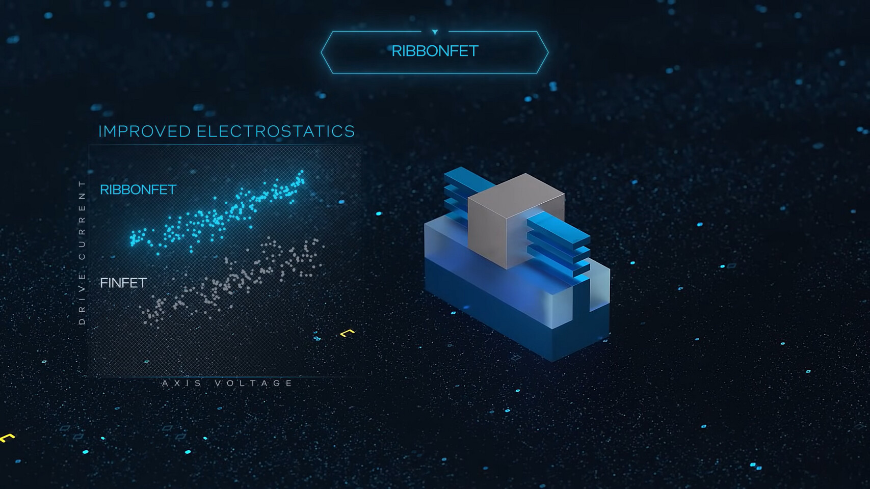
TSMC's Fab 21 Phase 2 facility is currently under construction in the Greater Phoenix area, Arizona—this secondary production facility was originally announced as housing a 3 nm process production line (opening by 2026), but that company target will be missed by a sizable margin. The transcription of the company's Q4 2023 Earnings Call presents another set of shifted expectations—outgoing CEO, Dr. Mark Liu—admitted that a number of factors are expected to delay Phase 2's opening by another year or two: "The second fab shell is under construction, but what technology [to use] in that shell is still under discussion...I think that also has to do with how much incentives that fab, the U.S. Government can provide…The current planning [for the fab] is '27 or '28, that will be timeframe."

Industry analysts believe TSMC leadership have a tough choice to make—the second Arizona factory's delayed launch could provide enough lead time to upgrade with a more advanced node (e.g. 2 nm), but ambitions could be lowered for the troubled site. An older plus more mature fabrication process could be a better fit, although the neighboring Fab 21 Phase 1 site is already set for a full 2025 initiation on 4 nm FinFET. Liu outlined this challenge: "To be honest, most of the overseas fabs, what technology is being set up, really, it is a decision of customers' demand in that area at that timing. So, nothing is definitive, but we are trying to optimize value for the overseas fab for TSMC." The current chairman will not be around for Phase 1's full deployment, but he shared some positive Arizona-related news: "We are well on track for volume production of N4, or 4 nm process technology, in the first half of 2025 [in Arizona] and are confident that once we begin operations, we will be able to deliver the same level of manufacturing quality and reliability in Arizona as from our fabs in Taiwan."

Not Just TSMC, Even Samsung Running Behind Schedule with its U.S. Fab

Delays in the construction of its U.S. based semiconductor fab may have just cost the Chairman of TSMC his job, but the Koreans aren't faring any better. BusinessKorea reports that Samsung Electronics has pushed the timeline for mass-production in its upcoming Austin Texas-based fab to 2025. Its construction was originally slated to be complete by now, with risk production and testing through early 2024, and mass production later in the year, which has all been pushed to 2025. The company now hopes to push its first wafer toward the end of 2024, with mass production expected some time in 2025.

Samsung reportedly blames issues with U.S. Government subsidies and regulatory problems behind the delays. A key aspect of getting cutting edge Asian foundries such as TSMC and Samsung to invest in the U.S. had to do with government subsidies to help these fabs overcome the uphill task of doing so Stateside and making the venture profitable. The U.S. had a sense of urgency in bringing these companies over, as it saw a potential conflict across the Taiwan straits, which threatened to disrupt practically the entire global digital economy. The company's first production line in this foundry was expected to be 4 nm EUV FinFET. It remains to be seen just how relevant and cutting edge 4 nm EUV is in 2025, as both TSMC and Intel hope to have Nanosheet transistors and nodes such as the TSMC N2 and Intel 20A taking shape by then.

IBM Demonstrates a Nanosheet Transistor that Loves 77 Kelvin—Boiling Point of Nitrogen

IBM, at the 2023 IEEE International Electron Device Meeting (IEDM), demonstrated a concept nanosheet transistor that posts a near 100% performance improvement at the boiling point of nitrogen, of 77 Kelvin (-196 °C). Given how relatively industrialized and scaled out the manufacture, safe transport, storage, and use of liquid nitrogen is, this development potentially unlocks a new class of chips that attain top performance under liquid nitrogen cooling. Think a new generation of AI HPC accelerators that can instantly double their performance under LN2, provided a new kind of cooling solution is developed for data-centers.

Nanosheet transistors are the evolutionary next step to FinFETs, which have been driving semiconductor foundries since 16 nm, which could see their technical limits met at 3 nm. Nanosheets are expected to make their debut with 2 nm-class nodes such as the TSMC N2 and Intel 20A. At an operating temperature of 77 K, IBM's nanosheet device is claimed to offer a near doubling in performance, due to less charge carrier scattering, which results in lower power. Reducing scattering reduces resistance in the wires, letting electrons move through the device more quickly. Combined with lower power, devices can drive a higher current at a given voltage. Cooling also results in greater sensitivity between the device's on and off positions, so it takes lesser power to switch between the two states, resulting in lower power. This lower power means that transistor widths can be lowered, resulting in higher transistor densities, or smaller chips. As of now IBM is wrestling with a technical challenge concerning the transistor's threshold voltage, a voltage which is needed to create a conducting channel between the source and the drain.

Intel, TSMC, and Samsung, Demo CFETs at IEEE IEDM Conference, Near Doubling in Transistor Densities in Sight

Last week at the IEEE International Electron Devices Meeting, the world's top-three semiconductor foundries, TSMC, Intel (Intel Foundry Services or IFS), and Samsung Electronics, demonstrated their respective approaches to an evolutionary new transistor device called the CFET, or complementary field-effect transistors. A CFET is a kind of 3-D transistor that stacks both kinds of FETs needed for CMOS logic. All three fabs are transitioning from FinFET to nanosheets, or GAAFETs (gates all-around FETs).

While FinFETs use vertical silicon fins, with gates controlling the flow of current through them; while in a nanosheet, the vertical fin is cut into a set of ribbons, each surrounded by the gate. A CFET is essentially a taller nanosheet device in which uses half of the available ribbons for one device, and the other half for another. This device builds the two types of transistor, nFETs and pFETs on top of each other, in an integrated process. CFETs are the evolutionary next step to conventional GAAFETs, and it's predicted to enter mass production only 7-10 years from now. By that time, the industry will begin to feel the pushback from technological barriers preventing development beyond 10 angstrom-class nodes.

Intel Demos 3D Transistors, RibbonFET, and PowerVia Technologies

During the 69th annual IEEE International Electron Devices Meeting (IEDM), Intel demonstrated some of its latest transistor design and manufacturing advancements. The first one in line is the 3D integration of transistors. According to Intel, the company has successfully stacked complementary field effect transistors (CFET) at a scaled gate pitch down to 60 nm. With CFETs promising thinner gate channels, the 3D stacked CFET would allow for higher density by going vertically and horizontally. Intel's 7 node has a 54 nm gate pitch, meaning CFETs are already close to matching production-ready nodes. With more time and development, we expect to see 3D stacked CFETs in the production runs in the coming years.

Next, Intel has demonstrated RibbonFET technology, a novel approach that is the first new transistor architecture since the introduction of FinFET in 2012. Using ribbon-shaped channels surrounded by the gate, these transistors allow for better control and higher drive current at all voltage levels. This allows faster transistor switching speeds, which later lead to higher frequency and performance. The width of these nanoribbon channels can be modulated depending on the application, where low-power mobile applications use less current, making the channels thinner, and high-performance applications require more current, making the channels wider. One stack of nanoribbons can achieve the same drive current as multiple fins found in FinFET but at a smaller footprint.

Samsung and TSMC Reportedly Struggling with 3 nm Yields

According to Korean business news publication ChosunBiz, both Samsung and TSMC are struggling with their 3 nm node yields. The two companies have different approaches to their 3 nm nodes, with Samsung using GAA FET (Gate All Around), whereas TSMC is continuing with its FinFET technology. That said, TSMC has at least five known 3 nm nodes, of which two should be in production by now, assuming N3E has proved to be reliable enough to kick off. Samsung on the other hand has three known 3 nm nodes, with only one in production so far, called 3GAE.

ChosunBiz reports that neither company is getting the kind of yields that you'd expect from a node that should have been in volume production for around a year by now, with Samsung apparently being somewhat better than TSMC. At 60 and 50 percent respectively, neither Samsung nor TSMC are anywhere near decent yields. Anything below 70 percent is considered very poor and even the 60 percent claim in Samsungs case, is apparently limited to some kind of Chinese mining ASIC and doesn't include the SRAM you find in most modern processors. ChosunBiz also mentions a source familiar with Samsung's foundry business who mentions a yield closer to 50 percent for the company. The same source also mentions that Samsung needs to reach at least 70 percent yield to be able to attract major customers to its 3 nm node.

TSMC Could Delay 2 nm Mass Production to 2026

According to TechNews.tw, TSMC could postpone its 2 nm semiconductor manufacturing node for 2026. If the rumors about TSMC's delayed 2 nm production schedule are accurate, the implications could reverberate throughout the semiconductor industry. TSMC's alleged hesitancy could be driven by multiple factors, including the architectural shift from FinFET to Gate-All-Around (GAA) and potential challenges related to scaling down to 2 nm. The company is a crucial player in this space, and a delay could offer opportunities for competitors like Samsung, which has already transitioned to GAA transistor architecture for its 3 nm chips. Given the massive demand for advanced nodes due to the rise of AI, IoT, and other next-gen technologies, it is surprising to hear "sluggish" demand reports.

However, it's also possible that it's too early for customers to make firm commitments for 2025 and beyond. TSMC has dismissed these rumors, stating that construction is progressing according to plan, which includes having 2 nm pilot run in 2024, and mass production in the second half of 2025.. Despite this, any delay in TSMC's roadmap could serve as a catalyst for shifts in market dynamics. Companies that rely heavily on TSMC's advanced nodes might need to reassess their timelines and strategies. Moreover, if Samsung can capitalize on this opportunity, it could somewhat level the playing field. As of now, though, it's essential to approach these rumors with caution until more concrete information becomes available.

TSMC is Building a $10B Fab In Germany

TSMC (TWSE: 2330, NYSE: TSM), Robert Bosch GmbH, Infineon Technologies AG (FSE: IFX / OTCQX: IFNNY), and NXP Semiconductors N.V. (NASDAQ: NXPI) today announced a plan to jointly invest in European Semiconductor Manufacturing Company (ESMC) GmbH, in Dresden, Germany to provide advanced semiconductor manufacturing services. ESMC marks a significant step towards construction of a 300 mm fab to support the future capacity needs of the fast-growing automotive and industrial sectors, with the final investment decision pending confirmation of the level of public funding for this project. The project is planned under the framework of the European Chips Act.

The planned fab is expected to have a monthly production capacity of 40,000 300 mm (12-inch) wafers on TSMC's 28/22 nanometer planar CMOS and 16/12 nanometer FinFET process technology, further strengthening Europe's semiconductor manufacturing ecosystem with advanced FinFET transistor technology and creating about 2,000 direct high-tech professional jobs. ESMC aims to begin construction of the fab in the second half of 2024 with production targeted to begin by the end of 2027.

Samsung Claims Higher 3 nm Yields than TSMC

Competition between Samsung and TSMC in the 4 nm and 3 nm foundry process markets is about to heat up, with the Korean foundry claiming yields competitive to those of TSMC, according to a report in the Kukmin Ilbo, a Korean daily newspaper. 4 nm is the final silicon fabrication process to use the FinFET technology that powered nodes ranging between 16 nm to 4 nm. Samsung Foundry is claiming 4 nm wafer yields of 75%, against the 80% yields figure put out by TSMC. 4 nm powers several current-generation mobile SoCs, PC processors, and more importantly, the GPUs driving the AI gold-rush.

Things get very interesting with 3 nm, the node that debuts GAA-FET (gates all around FET) technology. Here, Samsung claims to offer higher yields than TSMC, with its 3 nm GAA node clocking 60% yields, against 55% put out by TSMC. Samsung was recently bitten by a scandal where its engineers allegedly falsified yields figures to customers to score orders, which had a cascading effect on the volumes and competitiveness of their customers. We're inclined to think that Samsung has taken lessons and is more careful with the yields figures being reported in the press. Meanwhile, Intel Foundry Services competes with the Intel 3 node, which is physically 7 nm FinFET, but with electrical characteristics comparable to those of 3 nm.

TSMC CFET Transistors in the Lab, Still Many Generations Away

During the European Technology Symposium 2023, TSMC presented additional details regarding the upcoming complementary FET (CFET) technology to power the next generation of silicon-based devices. With Nanosheet replacing FinFET, the CFET technology will do the same to the Gate All Around FET (GAAFET) Nanosheet nodes. As the company notes, CFET transistors are now in the TSMC labs and are being tested for performance, efficiency, and density. Compared to GAAFET, CFET will provide greater design in all of those areas, but it will require some additional manufacturing steps to get the chip working as intended. Integrating both p-type and n-type FETs into a single device, CFET will require the use of High NA EUV scanners with high precision and high power to manufacture it.

The use of CFET, as the roadmap shows, is one of the last steps in the world of silicon. It will require the integration of new materials into the manufacturing process, resulting in a greater investment into research and development that is in charge of node creation. Kevin Zhang, senior vice president at TSMC, responsible for technology roadmap and business development, notes: "Let me make a clarification on that roadmap, everything beyond the Nanosheet is something we will put on our [roadmap] to tell you there is still future out there. We will continue to work on different options. I also have the add on to the one-dimensional material-[based transistors] […], all of those are being researched on being investigated on the future potential candidates right now, we will not tell you exactly the transistor architecture will be beyond the Nanosheet."

Samsung to Detail SF4X Process for High-Performance Chips

Samsung has invested heavily in semiconductor manufacturing technology to provide clients with a viable alternative to TSMC and its portfolio of nodes spanning anything from mobile to high-performance computing (HPC) applications. Today, we have information that Samsung will present its SF4X node to the public in this year's VLSI Symposium. Previously known as a 4HPC node, it is designed as a 4 nm-class node with a specialized use case for HPC processors, in contrast to the standard SF4 (4LPP) node that uses 4 nm transistors designed for low-power standards applicable to mobile/laptop space. According to the VLSI Symposium schedule, Samsung is set to present more info about the paper titled "Highly Reliable/Manufacturable 4nm FinFET Platform Technology (SF4X) for HPC Application with Dual-CPP/HP-HD Standard Cells."

As the brief introduction notes, "In this paper, the most upgraded 4nm (SF4X) ensuring HPC application was successfully demonstrated. Key features are (1) Significant performance +10% boosting with Power -23% reduction via advanced SD stress engineering, Transistor level DTCO (T-DTCO) and [middle-of-line] MOL scheme, (2) New HPC options: Ultra-Low-Vt device (ULVT), high speed SRAM and high Vdd operation guarantee with a newly developed MOL scheme. SF4X enhancement has been proved by a product to bring CPU Vmin reduction -60mV / IDDQ -10% variation reduction together with improved SRAM process margin. Moreover, to secure high Vdd operation, Contact-Gate breakdown voltage is improved by >1V without Performance degradation. This SF4X technology provides a tremendous performance benefits for various applications in a wide operation range." While we have no information on the reference for these claims, we suspect it is likely the regular SF4 node. More performance figures and an in-depth look will be available on Thursday, June 15, at Technology Session 16 at the symposium.

Intel 20A and 18A Foundry Nodes Complete Development Phase, On Track for 2024 Manufacturing

Intel Foundry Services, the in-house semiconductor foundry of Intel, announced that its 2 nm-class Intel 20A and 1.8 nm-class Intel 18A foundry nodes have completed development, and are on course for mass-producing chips on their roadmap dates. Chips are expected to begin mass-production on the Intel 20A node in the first half of 2024, while those on the Intel 18A node are expected to begin in the second half of 2024. The completion of the development phase means that Intel has finalized the specifications and performance/power targets of the nodes, the tools and software required to make the chips, and can now begin ordering them to build the nodes. Intel has been testing these nodes through 2022, and with the specs being finalized, chip-designers can accordingly wrap up development of their products to align with what these nodes have to offer.

Intel 20A (or 20-angstrom, or 2 nm) node introduces gates-all-around (GAA) RibbonFET transistors with PowerVIAs (an interconnect innovation that contributes to transistor densities). The Intel 20A node is claimed to offer a 15% performance/Watt gain over its predecessor, the Intel 3 node (FinFET EUV, 3 nm-class), which by itself offers an 18% performance/Watt gain over Intel 4 (20% perf/Watt gain over the current Intel 7 node), the node that is entering mass-production very soon. The Intel 18A node is a further refinement of Intel 20A, and introduces a design improvement to the RibbonFET that increases transistor density at scale, and a claimed 10% performance/Watt improvement over Intel 20A.

Phison E26 Controller Powering Several Upcoming PCIe Gen 5 NVMe SSDs Detailed

At the 2023 International CES, we caught a hold of Phison, makes or arguably the most popular SSD controllers, which sprung to prominence on being the first to market with PCIe Gen 4 NVMe controllers, and now hopes to repeat it with PCIe Gen 5. We'd been shown a reference-design Phison E26-powered M.2 SSD, along with some hardware specs of the controller itself. The drive itself isn't much to look at—a standard looking M.2-2280 drive with a PCI-Express 5.0 x4 host interface, and the Phison E26 controller with its shiny IHS being prominently located next to a DDR4 memory chip, and two new-generation Micron Technology 3D NAND flash memory chips.

The Phison E26 controller, bearing the long-form model number PS5026-E26, is an NVMe 2.0 spec client-segment SSD controller. It has been built on the TSMC 12 nm FinFET silicon-fabrication node. The controller features an integrated DRAM controller with support for DDR4 and LPDDR4 memory types for use as DRAM cache. Its main flash interface is 8-channel with 32 NAND chip-enable (CE) lines, support for TLC and QLC NAND flash, a dual-CPU architecture, and hardware-acceleration for AES-256, TCG-Opal, and Pyrite. The controller features Phison's 5th generation LPDC ECC and internal RAID engines. For its reference-design 2 TB TLC-based drive, Phison claims sequential transfer rates of up to 13.5 GB/s reads, with up to 12 GB/s writes. The 4K random-access performance is rated at up to 1.5 million IOPS reads, with up to 2 million IOPS writes.

Intel Research Fuels Moore's Law and Paves the Way to a Trillion Transistors by 2030

Today, Intel unveiled research breakthroughs fueling its innovation pipeline for keeping Moore's Law on track to a trillion transistors on a package in the next decade. At IEEE International Electron Devices Meeting (IEDM) 2022, Intel researchers showcased advancements in 3D packaging technology with a new 10x improvement in density; novel materials for 2D transistor scaling beyond RibbonFET, including super-thin material just 3 atoms thick; new possibilities in energy efficiency and memory for higher-performing computing; and advancements for quantum computing.

"Seventy-five years since the invention of the transistor, innovation driving Moore's Law continues to address the world's exponentially increasing demand for computing. At IEDM 2022, Intel is showcasing both the forward-thinking and concrete research advancements needed to break through current and future barriers, deliver to this insatiable demand, and keep Moore's Law alive and well for years to come." -Gary Patton, Intel vice president and general manager of Components Research and Design Enablement

AMD Explains the Economics Behind Chiplets for GPUs

AMD, in its technical presentation for the new Radeon RX 7900 series "Navi 31" GPU, gave us an elaborate explanation on why it had to take the chiplets route for high-end GPUs, devices that are far more complex than CPUs. The company also enlightened us on what sets chiplet-based packages apart from classic multi-chip modules (MCMs). An MCM is a package that consists of multiple independent devices sharing a fiberglass substrate.

An example of an MCM would be a mobile Intel Core processor, in which the CPU die and the PCH die share a substrate. Here, the CPU and the PCH are independent pieces of silicon that can otherwise exist on their own packages (as they do on the desktop platform), but have been paired together on a single substrate to minimize PCB footprint, which is precious on a mobile platform. A chiplet-based device is one where a substrate is made up of multiple dies that cannot otherwise independently exist on their own packages without an impact on inter-die bandwidth or latency. They are essentially what should have been components on a monolithic die, but disintegrated into separate dies built on different semiconductor foundry nodes, with a purely cost-driven motive.

Intel and MediaTek Form Foundry Partnership

Intel and MediaTek today announced a strategic partnership to manufacture chips using Intel Foundry Services' (IFS) advanced process technologies. The agreement is designed to help MediaTek build a more balanced, resilient supply chain through the addition of a new foundry partner with significant capacity in the United States and Europe. MediaTek plans to use Intel process technologies to manufacture multiple chips for a range of smart edge devices. IFS offers a broad manufacturing platform with technologies optimized for high performance, low power and always-on connectivity built on a roadmap that spans production-proven three-dimensional FinFET transistors to next-generation breakthroughs.

"As one of the world's leading fabless chip designers powering more than 2 billion devices a year, MediaTek is a terrific partner for IFS as we enter our next phase of growth," said IFS President Randhir Thakur. "We have the right combination of advanced process technology and geographically diverse capacity to help MediaTek deliver the next billion connected devices across a range of applications."

Samsung Begins Chip Production Using 3nm Process Technology With GAA Architecture

Samsung Electronics, the world leader in semiconductor technology, today announced that it has started initial production of its 3-nanometer (nm) process node applying Gate-All-Around (GAA) transistor architecture. Multi-Bridge-Channel FET (MBCFET), Samsung's GAA technology implemented for the first time ever, defies the performance limitations of FinFET, improving power efficiency by reducing the supply voltage level, while also enhancing performance by increasing drive current capability. Samsung is starting the first application of the nanosheet transistor with semiconductor chips for high performance, low power computing application and plans to expand to mobile processors.

"Samsung has grown rapidly as we continue to demonstrate leadership in applying next-generation technologies to manufacturing, such as foundry industry's first High-K Metal Gate, FinFET, as well as EUV. We seek to continue this leadership with the world's first 3 nm process with the MBCFET," said Dr. Siyoung Choi, President and Head of Foundry Business at Samsung Electronics. "We will continue active innovation in competitive technology development and build processes that help expedite achieving maturity of technology."

Intel Breakthroughs Propel Moore's Law Beyond 2025

In its relentless pursuit of Moore's Law, Intel is unveiling key packaging, transistor and quantum physics breakthroughs fundamental to advancing and accelerating computing well into the next decade. At IEEE International Electron Devices Meeting (IEDM) 2021, Intel outlined its path toward more than 10x interconnect density improvement in packaging with hybrid bonding, 30% to 50% area improvement in transistor scaling, major breakthroughs in new power and memory technologies, and new concepts in physics that may one day revolutionize computing.

"At Intel, the research and innovation necessary for advancing Moore's Law never stops. Our Components Research Group is sharing key research breakthroughs at IEDM 2021 in bringing revolutionary process and packaging technologies to meet the insatiable demand for powerful computing that our industry and society depend on. This is the result of our best scientists' and engineers' tireless work. They continue to be at the forefront of innovations for continuing Moore's Law," said Robert Chau, Intel Senior Fellow and general manager of Components Research.

TrendForce: Annual Foundry Revenue Expected to Reach Historical High Again in 2022 with 13% YoY Increase with Chip Shortage Showing Sign of Easing

While the global electronics supply chain experienced a chip shortage, the corresponding shortage of foundry capacities also led various foundries to raise their quotes, resulting in an over 20% YoY increase in the total annual revenues of the top 10 foundries for both 2020 and 2021, according to TrendForce's latest investigations. The top 10 foundries' annual revenue for 2021 is now expected to surpass US$100 billion. As TSMC leads yet another round of price hikes across the industry, annual foundry revenue for 2022 will likely reach US$117.69 billion, a 13.3% YoY increase.

TrendForce indicates that the combined CAPEX of the top 10 foundries surpassed US$50 billion in 2021, a 43% YoY increase. As new fab constructions and equipment move-ins gradually conclude next year, their combined CAPEX for 2022 is expected to undergo a 15% YoY increase and fall within the US$50-60 billion range. In addition, now that TSMC has officially announced the establishment of a new fab in Japan, total foundry CAPEX will likely increase further next year. TrendForce expects the foundry industry's total 8-inch and 12-inch wafer capacities to increase by 6% YoY and 14% YoY next year, respectively.

Samsung Foundry Announces GAA Ready, 3nm in 2022, 2nm in 2025, Other Speciality Nodes

Samsung Electronics, a world leader in advanced semiconductor technology, today unveiled plans for continuous process technology migration to 3- and 2-nanometer (nm) based on the company's Gate-All-Around (GAA) transistor structure at its 5th annual Samsung Foundry Forum (SFF) 2021. With a theme of "Adding One More Dimension," the multi-day virtual event is expected to draw over 2,000 global customers and partners. At this year's event, Samsung will share its vision to bolster its leadership in the rapidly evolving foundry market by taking each respective part of foundry business to the next level: process technology, manufacturing operations, and foundry services.

"We will increase our overall production capacity and lead the most advanced technologies while taking silicon scaling a step further and continuing technological innovation by application," said Dr. Siyoung Choi, President and Head of Foundry Business at Samsung Electronics. "Amid further digitalization prompted by the COVID-19 pandemic, our customers and partners will discover the limitless potential of silicon implementation for delivering the right technology at the right time."

Foundry Revenue for 2Q21 Reaches Historical High Once Again with 6% QoQ Growth Thanks to Increased ASP and Persistent Demand, Says TrendForce

The panic buying of chips persisted in 2Q21 owing to factors such as post-pandemic demand, industry-wide shift to 5G telecom technology, geopolitical tensions, and chronic chip shortages, according to TrendForce's latest investigations. Chip demand from ODMs/OEMs remained high, as they were unable to meet shipment targets for various end-products due to the shortage of foundry capacities. In addition, wafers inputted in 1Q21 underwent a price hike and were subsequently outputted in 2Q21. Foundry revenue for the quarter reached US$24.407 billion, representing a 6.2% QoQ increase and yet another record high for the eighth consecutive quarter since 3Q19.

Intel Accelerates Packaging and Process Innovations

Intel Corporation today revealed one of the most detailed process and packaging technology roadmaps the company has ever provided, showcasing a series of foundational innovations that will power products through 2025 and beyond. In addition to announcing RibbonFET, its first new transistor architecture in more than a decade, and PowerVia, an industry-first new backside power delivery method, the company highlighted its planned swift adoption of next-generation extreme ultraviolet lithography (EUV), referred to as High Numerical Aperture (High NA) EUV. Intel is positioned to receive the first High NA EUV production tool in the industry.

"Building on Intel's unquestioned leadership in advanced packaging, we are accelerating our innovation roadmap to ensure we are on a clear path to process performance leadership by 2025," Intel CEO Pat Gelsinger said during the global "Intel Accelerated" webcast. "We are leveraging our unparalleled pipeline of innovation to deliver technology advances from the transistor up to the system level. Until the periodic table is exhausted, we will be relentless in our pursuit of Moore's Law and our path to innovate with the magic of silicon."
Return to Keyword Browsing
May 1st, 2024 08:43 EDT change timezone

New Forum Posts

Popular Reviews

Controversial News Posts