Tuesday, June 23rd 2020

Intel Plans to Volume Manufacture Nanowire/Nanoribbon Transistors in Five Years
Semiconductor manufacturing is a hard business. There is a constant need for manufacturers to compete with each other and if they don't, they get left behind. Intel, as one of the biggest semiconductor makers in the world, is always trying to invent new technologies spending massive R&D funds on semiconductors. New technologies such as nanowire/nanoribbon transistors, which are supposed to enable transistor sizes unimaginable now, are on its way to make it in the hand of consumers. During the international VLSI conference, Intel's CTO Mike Mayberry held a presentation about how Intel plans to address the demand for more compute by showing off new technologies.
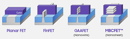
With a presentation titled "The Future of Compute", Mr. Mayberry made some exciting claims and predictions. So far, we have been used to FinFET transistors since the 22 nm node from Intel. However, as nodes get smaller the gate of the transistor is not enough to keep it from switching randomly. So to avoid that problem Intel, along with other semiconductor manufacturers like Samsung, created a solution called Gate-All-Around FET (GAAFET). This technology takes a transistor fin and wraps in around all sides (see picture below), so the gate has better switching control, preventing random switching and errors. As a fin, nanowire or nanosheet (wider option from nanowire) can be used and they can be stacked. These allow for additional control of tailoring whatever a node will be used for high performance or low power. Intel predicts that they will start high volume manufacturing of silicon based on this technology in five years. This is setting an important milestone for Intel as well as other industry players, as now everyone will rush to deliver it first. It is now a waiting game to see who will actually come out with it first.
Source:
AnandTech
With a presentation titled "The Future of Compute", Mr. Mayberry made some exciting claims and predictions. So far, we have been used to FinFET transistors since the 22 nm node from Intel. However, as nodes get smaller the gate of the transistor is not enough to keep it from switching randomly. So to avoid that problem Intel, along with other semiconductor manufacturers like Samsung, created a solution called Gate-All-Around FET (GAAFET). This technology takes a transistor fin and wraps in around all sides (see picture below), so the gate has better switching control, preventing random switching and errors. As a fin, nanowire or nanosheet (wider option from nanowire) can be used and they can be stacked. These allow for additional control of tailoring whatever a node will be used for high performance or low power. Intel predicts that they will start high volume manufacturing of silicon based on this technology in five years. This is setting an important milestone for Intel as well as other industry players, as now everyone will rush to deliver it first. It is now a waiting game to see who will actually come out with it first.


19 Comments on Intel Plans to Volume Manufacture Nanowire/Nanoribbon Transistors in Five Years
5 years later, they are still struggling with it.
So...yeah...Intel nanowire in 2030. Maybe.
Is someone counting? Is that dedicated Intel feed up yet?
Does anyone care yet? :D
It's going to take a fair few steps to get them produced, even with EUV.
Intel in 5 years: Here's our latest manufacturing innovation in production: 14nm++++++++++++++++++++++!
Engineering? Not so much.
Transistor Gate Pitch is 68nm, the Interconnect pitch is 51nm, the Transistor Fin Pitch is 42nm and Transistor Fin Height is 49nm.