News Posts matching #VLSI

Return to Keyword Browsing

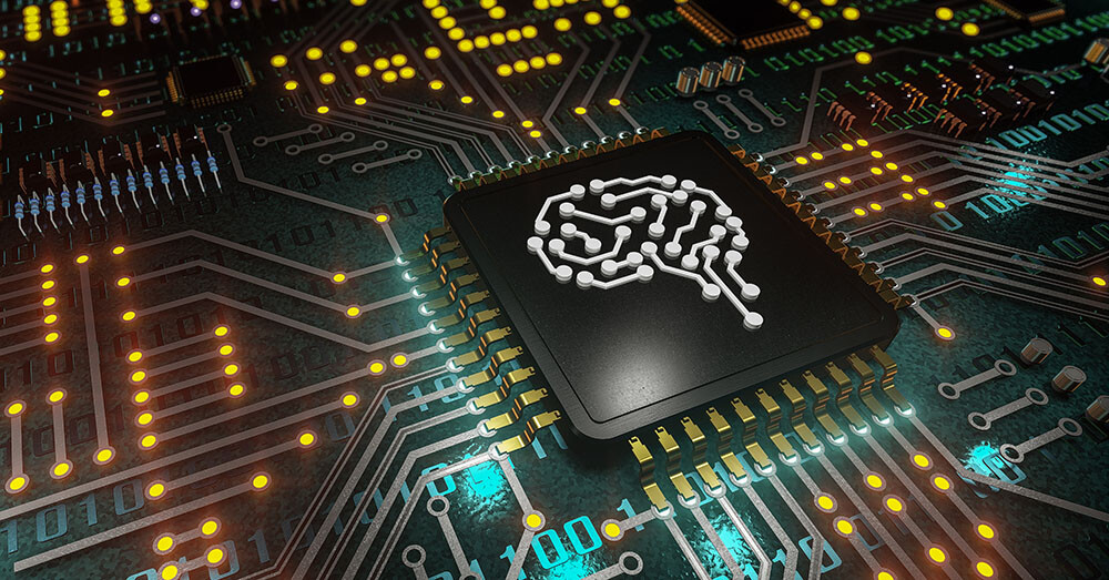
Jim Keller Offers to Design AI Chips for Sam Altman for Less Than $1 Trillion

In case you missed it, Sam Altman of OpenAI took the Internet by storm late last week with the unveiling of Sora, the generative AI that can congure up photoreal video clips based on prompts, with deadly accuracy. While Altman and his colleagues in the generative AI industry had a ton of fun generating videos based on prompts from the public on X; it became all too clear that the only thing holding back the democratization of generative AI is the volume of AI accelerator chips. Altman wants to solve this by designing his own AI acceleration hardware from the grounds up, for which he initially pitched an otherworldly $7 trillion in investment—something impossible with the financial markets, but one that's possible only by "printing money," or through sovereign wealth fund investments.

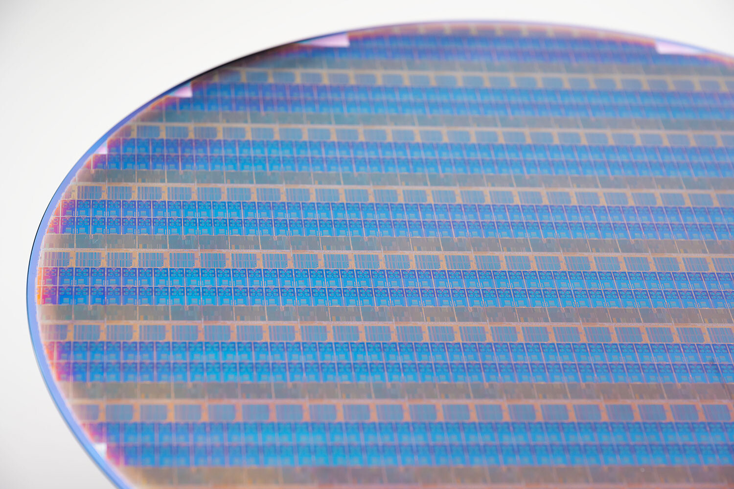
Jim Keller needs no introduction—the celebrity VLSI architect has been designing number crunching devices of all shapes and sizes for some of the biggest tech companies out there for decades, including Intel, Apple, and AMD, just to name a few. When as part of his "are you not entertained?" victory lap, Altman suggested that his vision for the future needs an even larger $8 trillion investment, Keller responded that he could design an AI chip for less than $1 trillion. Does Altman really need several trillions of Dollars to build a grounds-up AI chip at the costs and volumes needed to mainstream AI?

Court Overturns $2.18 Billion VLSI Patent Infringement Verdict, But Still Not Over For Intel

A U.S. appeals court has overturned a staggering $2.18 billion patent infringement verdict against Intel Corporation, initially won by VLSI Technology, marking a pivotal shift in one of the most prominent patent law cases in U.S. history. The 2021 decision by a Texas jury, which found Intel guilty of infringing on a VLSI patent, was reversed by the U.S. Court of Appeals for the Federal Circuit due to insufficient evidence. Additionally, a new trial in Texas has been ordered to determine the appropriate amount Intel owes for infringing a second patent owned by VLSI. This patent-holding company, affiliated with Fortress Investment Group and recently involved in a majority share acquisition by Abu Dhabi's Mubadala Investment Co from Japan's Softbank, has been in multiple legal confrontations with Intel over semiconductor technology patents, which VLSI acquired from NXP Semiconductors.

The legal disputes have seen varied outcomes; Intel deflected a claim for more than $3 billion in damages in a separate Waco jury trial in 2021. However, the same year, VLSI was awarded nearly $949 million from Intel in another patent case by a jury in Austin, Texas. The companies mutually agreed to dismiss another potential multi-billion-dollar lawsuit in Delaware. With Intel's stock experiencing a downturn (-6.05% in the past five days) following the latest court ruling and the scheduled 2024 trial in Northern California, the ongoing legal battles between the two tech entities continue to influence market dynamics and the semiconductor industry at large. Detaining if the patent infringement happened is still relatively complex, as VLSI needs a team of engineers to determine if Intel used any of its patents.

US Patent Office Sides with Intel in the $2.2 Billion VLSI Case

The U.S. Patent Office tribunal has ruled in favor of Intel Corp in a significant $2.2 billion case against VLSI Technology LLC. Intel's bid to nullify a patent that constituted $1.5 billion of a $2.18 billion verdict it previously lost to VLSI in 2021 was accepted. The Patent Trial and Appeal Board invalidated the computer chip-related patent and another VLSI patent, accounting for the rest of the Texas federal court verdict. An Intel spokesperson expressed their satisfaction with the decision, criticizing the invalidated VLSI patents as "low-quality."

VLSI, the company holding the patent that has filed several infringement lawsuits against Intel, retains the option to appeal both decisions to the U.S. Court of Appeals for the Federal Circuit. In a separate case last year, VLSI secured a verdict worth $949 million against Intel in Texas. VLSI is a subsidiary of Fortress Investment Group, which is managed by investment funds from SoftBank Group. The patent board proceeding was initiated by South Dakota-based Patent Quality Assurance LLC, while another patent from the $2.18 billion verdict was contested by OpenSky Industries LLC. Despite initial sanctions for attempting to extort both Intel and VLSI, OpenSky was permitted to continue the proceeding with Intel at the helm.

With PowerVia, Intel Achieves a Chipmaking Breakthrough

Intel is about to turn chipmaking upside down with PowerVia, a new approach to delivering power that required a radical rethink to both how chips are made and how they are tested. For all the modern history of computer chips, they've been built like pizzas—from the bottom up, in layers. In the case of chips, you start with the tiniest features, the transistors, and then you build up increasingly less-tiny layers of wires that connect the transistors and different parts of the chip (these are called interconnects). Included among those top layers are the wires that bring in the power that makes the chip go.

When the chip is done, you flip it over, enclose it in packaging that provides connections to the outer world, and you're ready to put it in a computer. Unfortunately, this approach is running into problems. As they get smaller and denser, the layers that share interconnects and power connections have become an increasingly chaotic web that hinders the overall performance of each chip. Once an afterthought, "now they have a huge impact," says Ben Sell, vice president of Technology Development at Intel and part of the team that brought PowerVia to fruition. In short, power and signals fade, requiring workarounds or simply dumping more power in.

Samsung to Detail SF4X Process for High-Performance Chips

Samsung has invested heavily in semiconductor manufacturing technology to provide clients with a viable alternative to TSMC and its portfolio of nodes spanning anything from mobile to high-performance computing (HPC) applications. Today, we have information that Samsung will present its SF4X node to the public in this year's VLSI Symposium. Previously known as a 4HPC node, it is designed as a 4 nm-class node with a specialized use case for HPC processors, in contrast to the standard SF4 (4LPP) node that uses 4 nm transistors designed for low-power standards applicable to mobile/laptop space. According to the VLSI Symposium schedule, Samsung is set to present more info about the paper titled "Highly Reliable/Manufacturable 4nm FinFET Platform Technology (SF4X) for HPC Application with Dual-CPP/HP-HD Standard Cells."

As the brief introduction notes, "In this paper, the most upgraded 4nm (SF4X) ensuring HPC application was successfully demonstrated. Key features are (1) Significant performance +10% boosting with Power -23% reduction via advanced SD stress engineering, Transistor level DTCO (T-DTCO) and [middle-of-line] MOL scheme, (2) New HPC options: Ultra-Low-Vt device (ULVT), high speed SRAM and high Vdd operation guarantee with a newly developed MOL scheme. SF4X enhancement has been proved by a product to bring CPU Vmin reduction -60mV / IDDQ -10% variation reduction together with improved SRAM process margin. Moreover, to secure high Vdd operation, Contact-Gate breakdown voltage is improved by >1V without Performance degradation. This SF4X technology provides a tremendous performance benefits for various applications in a wide operation range." While we have no information on the reference for these claims, we suspect it is likely the regular SF4 node. More performance figures and an in-depth look will be available on Thursday, June 15, at Technology Session 16 at the symposium.

Intel to Demonstrate PowerVia on E-Core Processor Built with Intel 4 Node

At VLSI Symposium 2023, scheduled to take place between June 11-16, Intel is set to demonstrate its PowerVia technology working efficiently on an E-Core chip built using the Intel 4 node. Conventional chips have power and signal interconnects distributed across multiple metal layers. PowerVia, on the other hand, dedicates specific layers for power delivery, effectively separating them from the signal routing layers. This approach allows for vertical power delivery through a set of power-specific Through-Silicon Vias (TSVs) or PowerVias, which are essentially vertical connections between the top and bottom surfaces of the chip. By delivering power directly from the backside of the chip, PowerVia reduces power supply noise and resistive losses, optimizing power distribution and improving overall energy efficiency. PowerVia is set to make a debut in 2024 with Intel 20A node.

For VLSI Symposium 2023 talk, the company has prepared a paper that highlights a design made using Intel 4 technology and implements E-Cores only in a test chip. The document states: "PowerVia Technology is a novel innovation to extend Process Scaling by having Power Delivery on the backside. This paper presents the pre and post silicon findings from implementing an Intel E-Core in PowerVia Technology. PowerVia enabled standard cell utilization of greater than 90 percent in large areas of the core while showing greater than 5 percent frequency benefit in silicon due reduced IR drop. Successful Post silicon debug is demonstrated with slightly higher but acceptable throughput times. The thermal characteristics of the PowerVia testchip is inline with higher power densities expected from logic scaling."

Intel 4 Process Node Detailed, Doubling Density with 20% Higher Performance

Intel's semiconductors nodes have been quite controversial with the arrival of the 10 nm design. Years in the making, the node got delayed multiple times, and only recently did the general public get the first 10 nm chips. Today, at IEEE's annual VLSI Symposium, we get more details about Intel's upcoming nodes, called Intel 4. Previously referred to as a 7 nm process, Intel 4 is the company's first node to use EUV lithography accompanied by various technologies. The first thing when a new process node is discussed is density. Compared to Intel 7, Intel 4 will double the transistor count for the same area and enable 20% higher performing transistors.

Looking at individual transistor size, the new Intel 4 node represents a very tiny piece of silicon that is even smaller than its predecessor. With a Fin Pitch of 30 nm, Contact Gate Poly Pitch of 50 nm between gates, and Minimum Metal Pitch (M0) of 50 nm, the Intel 4 transistor is significantly smaller compared to the Intel 7 cell, listed in the table below. For scaling, Intel 4 provides double the number of transistors in the same area compared to Intel 7. However, this reasoning is applied only to logic. For SRAM, the new PDK provides 0.77 area reduction, meaning that the same SoC built on Intel 7 will not be half the size of Intel 4, as SRAM plays a significant role in chip design. The Intel 7 HP library can put 80 million transistors on a square millimeter, while Intel 4 HP is capable of 160 million transistors per square millimeter.

Intel "Meteor Lake-P" SoC with 6P+8E Compute Tile Pictured

Intel's next-generation "Meteor Lake-P" mobile processor with a 6P+8E Compute Tile was shown off at the 2022 IEEE VLSI Symposium on Tech and Circuits (6 performance cores and 8 efficiency cores). We now have annotations for all four tiles, as well as a close-up die-shot of the Compute Tile. Intel also confirmed that the Compute Tile will be built on its homebrew Intel 4 silicon fabrication process, which offers over 20% iso-power performance increase versus the Intel 7 node, through extensive use of EUV lithography.

We had earlier seen a 2P+8E version of the "Meteor Lake" Compute Tile, probably from the "Meteor Lake-U" package. The larger 6P+8E Compute tile features six "Redwood Cove" performance cores, and two "Crestmont" efficiency core clusters, each with four E-cores. Assuming the L3 cache slice per P-core or E-core cluster is 2.5 MB, there has to be 20 MB of L3 cache on the compute tile. Each P-core has 2 MB of dedicated L2 cache, while each of the two E-core clusters shares 4 MB of L2 cache among four E-cores.

Intel Fined 2 Billion USD In Damages For Patent Infringement

A federal jury in Texas has ruled that Intel Corporation violated two patents of VLSI Technology and must pay 2.18 billion USD in damages. The damages include 1.5 billion for one patent and 675 million for the other. The patents are related to clock frequency control and minimum memory operating voltage technique and were awarded to Freescale Semiconductor Inc in 2012 and SigmaTel in 2010. Freescale bought SigmaTel gaining control of the two patents before being passed to NXP after the company acquired Freescale in 2015, these patents were then transferred to the newly resurrected VLSI Technology in 2019 with the sole purpose of launching a legal battle against Intel. In a comment to Tom's Hardware the company said "Intel strongly disagrees with today's jury verdict. We intend to appeal and are confident that we will prevail.". This legal battle will likely drag-out for several years as Intel plans to appeal the recent ruling. Intel recorded a net income of 5.9 billion USD in Q4 2020 so this fine is by no means insignificant.

SoftBank Reportedly Considering Selling Arm Holdings

According to the report from The Wall Street Journal, we have obtained information that SoftBank, owner of Arm Holdings, is considering a future of Arm Holdings without SoftBank's ownership. The report is indicating that SoftBank can either sell its subsidiary or make it go to public with Initial Public Offering (IPO). If we recall, SoftBank has purchased Arm Holdings in 2016 for 32 billion USD, and the company is potentially worth much more today. Arm Holdings was established as a joint between Acorn Computers, Apple Computer (now Apple Inc.), and VLSI Technology. The news of SoftBank selling Arm Holdings is coming just after Apple decided to make a Mac based on Arm ISA.

The report from WSJ says that the market interest for such acquisition is unknown, so there is a big possibility that SoftBank will ultimately do nothing and just keep the company. My speculations could be that Apple may have an interest in the company since it is using its royalties and intellectual property. If such a thing happens Apple would be forced to sign a deal by antitrust regulators that force the company to continue offering to license the ISA. After all, Apple was one of the founding members of the joint venture. The possibility of that is of course very low. If another option such as IPO happens, the company would still be in ownership of SoftBank, it would just go to the public trading market.

Kioxia Plans for Wafer-Level SSD

Wafer-scale design is getting popular it seems. Starting from the wafer-scale engine presented by Cerebras last year, which caused quite the shakeup in the industry, it seems that this design approach might be more useful than anyone thought. During VLSI Symposium 2020, Shigeo Oshima, Chief Engineer at Kioxia, had a presentation about new developments in SSD designs and implementations. What was one of the highlights of the presentation was the information that Kioxia is working on, was a technology Kioxia is referring to as wafer-level SSD.

The NAND chips used in SSDs would no longer be cut from the wafer and packaged separately. Instead, the wafer itself would represent the SSD. This is a similar approach Cerebras used with its wafer-scale engine AI processor. What would be gains of this approach compared to traditional methods of cutting up NAND chips and packaging them separately you might wonder? Well, for starters you wouldn't need to cut the wafer, package individual memory chips, and build the SSD out of them. Those steps could be skipped and there would be some cost savings present. And imagine if you decide to do wafer stacking. You could build super scaling SSDs with immense performance capable of millions of IOPS. However, for now, this is only a concept and it is just in early development. There is no possibility to find it in a final product anytime soon.
Kioxia Wafer-Level SSD

Intel Plans to Volume Manufacture Nanowire/Nanoribbon Transistors in Five Years

Semiconductor manufacturing is a hard business. There is a constant need for manufacturers to compete with each other and if they don't, they get left behind. Intel, as one of the biggest semiconductor makers in the world, is always trying to invent new technologies spending massive R&D funds on semiconductors. New technologies such as nanowire/nanoribbon transistors, which are supposed to enable transistor sizes unimaginable now, are on its way to make it in the hand of consumers. During the international VLSI conference, Intel's CTO Mike Mayberry held a presentation about how Intel plans to address the demand for more compute by showing off new technologies.

With a presentation titled "The Future of Compute", Mr. Mayberry made some exciting claims and predictions. So far, we have been used to FinFET transistors since the 22 nm node from Intel. However, as nodes get smaller the gate of the transistor is not enough to keep it from switching randomly. So to avoid that problem Intel, along with other semiconductor manufacturers like Samsung, created a solution called Gate-All-Around FET (GAAFET). This technology takes a transistor fin and wraps in around all sides (see picture below), so the gate has better switching control, preventing random switching and errors. As a fin, nanowire or nanosheet (wider option from nanowire) can be used and they can be stacked. These allow for additional control of tailoring whatever a node will be used for high performance or low power. Intel predicts that they will start high volume manufacturing of silicon based on this technology in five years. This is setting an important milestone for Intel as well as other industry players, as now everyone will rush to deliver it first. It is now a waiting game to see who will actually come out with it first.
Intel Nanowire/Nanoribbon Samsung GAAFET

AMD "Renoir" Die Annotation Raises Hopes of Desktop Chips Featuring x16 PEG

VLSI engineer Fritzchens Fritz, famous for high-detail EM photography of silicon dies and annotations of them, recently published his work on AMD's 7 nm "Renoir" APU silicon. His die-shots were annotated by Nemez aka GPUsAreMagic. The floor-plan of the silicon shows that the CPU component finally dwarfs the iGPU component, thanks to double the CPU cores over the previous-gen "Picasso" silicon, spread over two CCXs (compute complexes). The CCX on "Renoir" is visibly smaller than the one on the "Zen 2" CCDs found in "Matisse" and "Rome" MCMs, as the L3 cache is smaller, at 4 MB compared to 16 MB. Being MCMs with disintegrated memory controllers, it makes more sense for CCDs to have more last-level cache per CCX.

We also see that the iGPU features no more than 8 "Vega" NGCUs, so there's no scope for "Renoir" based desktop APUs to feature >512 stream processors. AMD attempted to compensate for the NGCU deficit by dialing up engine clocks of the iGPU by over 40% compared to those on "Picasso." What caught our eye in the annotation is the PCI-Express physical layer. Apparently the die indeed has 20 PCI-Express lanes besides an additional 4 lanes that can be configured as two SATA 6 Gbps ports thanks to SerDes flexibility.

Intel Showcases Intelligent Edge and Energy-efficient Performance Research

This week at the 2020 Symposia on VLSI Technology and Circuits, Intel will present a body of research and technical perspectives on the computing transformation driven by data that is increasingly distributed across the core, edge and endpoints. Chief Technology Officer Mike Mayberry will deliver a plenary keynote, "The Future of Compute: How Data Transformation is Reshaping VLSI," that highlights the importance of transitioning computing from a hardware/program-centric approach to a data/information-centric approach.

"The sheer volume of data flowing across distributed edge, network and cloud infrastructure demands energy-efficient, powerful processing to happen close to where the data is generated, but is often limited by bandwidth, memory and power resources. The research Intel Labs is showcasing at the VLSI Symposia highlights several novel approaches to more efficient computation that show promise for a range of applications - from robotics and augmented reality to machine vision and video analytics. This body of research is focused on addressing barriers to the movement and computation of data, which represent the biggest data challenges of the future," said Vivek K. De, Intel fellow and director of Circuit Technology Research, Intel Labs.

TSMC and Broadcom Enhance the CoWoS Platform with World's First 2X Reticle Size Interposer

TSMC today announced it has collaborated with Broadcom on enhancing the Chip-on-Wafer-on-Substrate (CoWoS ) platform to support the industry's first and largest 2X reticle size interposer. With an area of approximately 1,700mm2, this next generation CoWoS interposer technology significantly boosts computing power for advanced HPC systems by supporting more SoCs as well as being ready to support TSMC's next-generation five-nanometer (N5) process technology.

This new generation CoWoS technology can accommodate multiple logic system-on-chip (SoC) dies, and up to 6 cubes of high-bandwidth memory (HBM), offering as much as 96 GB of memory. It also provides bandwidth of up to 2.7 terabytes per second, 2.7 times faster than TSMC's previously offered CoWoS solution in 2016. With higher memory capacity and bandwidth, this CoWoS solution is well-suited for memory-intensive workloads such as deep learning, as well as workloads for 5G networking, power-efficient datacenters, and more. In addition to offering additional area to increase compute, I/O, and HBM integration, this enhanced CoWoS technology provides greater design flexibility and yield for complex ASIC designs in advanced process nodes.
Return to Keyword Browsing
Apr 30th, 2024 18:22 EDT change timezone

New Forum Posts

Popular Reviews

Controversial News Posts