Monday, June 5th 2023

With PowerVia, Intel Achieves a Chipmaking Breakthrough
Intel is about to turn chipmaking upside down with PowerVia, a new approach to delivering power that required a radical rethink to both how chips are made and how they are tested. For all the modern history of computer chips, they've been built like pizzas—from the bottom up, in layers. In the case of chips, you start with the tiniest features, the transistors, and then you build up increasingly less-tiny layers of wires that connect the transistors and different parts of the chip (these are called interconnects). Included among those top layers are the wires that bring in the power that makes the chip go.
When the chip is done, you flip it over, enclose it in packaging that provides connections to the outer world, and you're ready to put it in a computer. Unfortunately, this approach is running into problems. As they get smaller and denser, the layers that share interconnects and power connections have become an increasingly chaotic web that hinders the overall performance of each chip. Once an afterthought, "now they have a huge impact," says Ben Sell, vice president of Technology Development at Intel and part of the team that brought PowerVia to fruition. In short, power and signals fade, requiring workarounds or simply dumping more power in.


 Two Problems, One Solution and "a Lot of Concerns and Hesitancy"
That's not to say Intel teams didn't foresee these issues—research and development on a new approach dates back a decade—nor does Intel face them alone. The solution that Intel and leading-edge chipmakers are all working toward is called "backside power," to find a way to move the power wires below the transistor to the "back" side of the chip and thus leave the interconnect or "front" side cleanly focused only on interconnection.
Seems pretty obvious, right? Why didn't we always do it this way? Two simple reasons: The old way is more straightforward to make and, as noted, it mostly wasn't an issue.
But Intel's got it figured out.
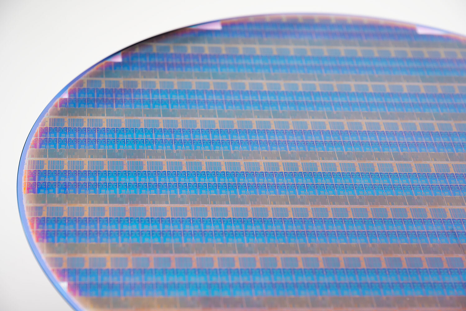
Intel's backside power solution is called PowerVia, and two new papers to be published at the 2023 VLSI Symposium show that Intel devised a process to manufacture it, test it and demonstrate positive performance results. The "test it" part is most important, but the manufacturing part is what's most surprising. Throw out pizza-making. For the first time, chipmaking is going two-sided.
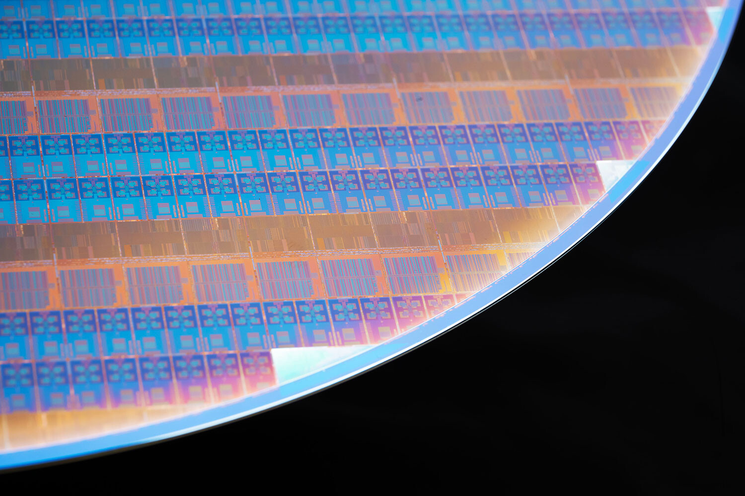
Here's how it works: Transistors are built first, as before, with the interconnect layers added next. Now the fun part: flip over the wafer and "polish everything off," Sell notes, to expose the bottom layer to which the wires (well, metal layers … all these "wires" are microscopic) for power will be connected. "We call it silicon technology," he adds, "but the amount of silicon that's left on these wafers is really tiny."
After the polish, "now you only have very few metal layers and they're all very thick," Sell explains—remember he lives in the land of nanometers, so "thick" means mere micrometers. That leaves "a very direct path for the power delivery to your transistor."
Cost, Performance and Power Benefits Outstrip Complexity
The benefits of this approach are manifold, Sell confirms, surpassing the added complexity of the new process.
The wires for power, for example, can take up to 20% of that front-side real estate, so with them gone, the interconnect layers can be "relaxed." "That more than offsets the cost of this whole big process," Sell notes, simplifying what had been the most tortuous portion of the manufacturing flow. The net effect is that the two-part flip-it-over process is actually cheaper than the old way.
The benefits aren't limited to manufacturing. The test chip the Intel team used to prove out the approach—called Blue Sky Creek and based on the Efficient-core (E-core) coming in Intel's forthcoming Meteor Lake processor for PCs—demonstrated that PowerVia solved both problems caused by the old pizza method. With separated and fatter wires for power and interconnection, "you get better power delivery and you get better signal wiring."
For your average computer user, this means more efficient speed. Get work done faster and with less power, the promise of Moore's Law delivered again. As the second paper dryly concludes, "The Intel E-core designed with PowerVia demonstrates >5% frequency improvement and >90% cell density with acceptable debug times as Intel 4." Sell confirms this is a "substantial" frequency boost for just moving wires around.
A Unique Test Chip with Intentional, Hidden Bugs
The last part of that conclusion—"acceptable debug times"—is a critical achievement alongside the product improvements. Today, chip-testing techniques are based on the accessibility of the transistors in that first and lowest layer. With the transistors now sandwiched in the middle of the chip, "a lot of those techniques had to be redeveloped," says Sell.
"There were a lot of concerns and hesitancy and that was probably the hardest thing to figure out—how to do debug on this new backside power delivery." To make things even more challenging, the test chip design team intentionally added some "Easter egg" errors to the chip, unbeknownst to the validation team. The good news? They found the bugs.
"We have made tremendous progress over the last couple of years in developing those debug capabilities and proving them on Blue Sky Creek," Sell asserts.
That brings up one more novel thing about how Sell and the Intel team figured out the PowerVia recipe. PowerVia will be introduced into Intel-manufactured silicon starting with the Intel 20A node, which enters production in 2024 (Intel 20A will also see the introduction of a new gate-all-around transistor design called RibbonFET; customers of Intel Foundry Services can benefit from both innovations in the subsequent Intel 18A node, arriving later in 2024). To isolate the development of PowerVia, they took the well-proven transistors from the preceding Intel 4 process node and built a special in-between node with the power and interconnect design planned for Intel 20A.
A Special Test Process Node to Isolate Backside Power
And while Intel manufacturing and design teams regularly create all manner of Frankenstein test-chips—to test new designs and intellectual properties and to solidify silicon processes—they don't usually make them as functional and complete as Blue Sky Creek. In this case, the teams needed to verify not only that they could build and test a chip this way, but also that the new configuration wouldn't bring new issues into the final product.
For instance, heat. "Normally you use the silicon side also for heat dissipation," Sell explains. "So now you have sandwiched your transistors and the question is, 'Do we have a thermal problem? Do we get a lot of local heating?'" At this point you can probably guess the answer: no.
"What was most amazing," Sell recalls, "was despite these radical changes"—sandwiching transistors in the middle of the chip and introducing this heavy "polishing" to the process—"we could make the transistors look very, very close to what we had in Intel 4."
As for PowerVia, it has no peer. According to recent reports, Intel's planned 2024 introduction of PowerVia would put competitors "roughly two years behind" when it comes to backside power.
"At least for this time period," confirms Sell, "we have a quite competitive backside power delivery option."
Your first opportunity to feel the many benefits of PowerVia will come next year in the form of Arrow Lake, a next-generation Intel processor for PCs built using the Intel 20A process. Its billions of transistors will be inverted, working more efficiently than ever.
When the chip is done, you flip it over, enclose it in packaging that provides connections to the outer world, and you're ready to put it in a computer. Unfortunately, this approach is running into problems. As they get smaller and denser, the layers that share interconnects and power connections have become an increasingly chaotic web that hinders the overall performance of each chip. Once an afterthought, "now they have a huge impact," says Ben Sell, vice president of Technology Development at Intel and part of the team that brought PowerVia to fruition. In short, power and signals fade, requiring workarounds or simply dumping more power in.
That's not to say Intel teams didn't foresee these issues—research and development on a new approach dates back a decade—nor does Intel face them alone. The solution that Intel and leading-edge chipmakers are all working toward is called "backside power," to find a way to move the power wires below the transistor to the "back" side of the chip and thus leave the interconnect or "front" side cleanly focused only on interconnection.
Seems pretty obvious, right? Why didn't we always do it this way? Two simple reasons: The old way is more straightforward to make and, as noted, it mostly wasn't an issue.
But Intel's got it figured out.
Intel's backside power solution is called PowerVia, and two new papers to be published at the 2023 VLSI Symposium show that Intel devised a process to manufacture it, test it and demonstrate positive performance results. The "test it" part is most important, but the manufacturing part is what's most surprising. Throw out pizza-making. For the first time, chipmaking is going two-sided.
Here's how it works: Transistors are built first, as before, with the interconnect layers added next. Now the fun part: flip over the wafer and "polish everything off," Sell notes, to expose the bottom layer to which the wires (well, metal layers … all these "wires" are microscopic) for power will be connected. "We call it silicon technology," he adds, "but the amount of silicon that's left on these wafers is really tiny."
After the polish, "now you only have very few metal layers and they're all very thick," Sell explains—remember he lives in the land of nanometers, so "thick" means mere micrometers. That leaves "a very direct path for the power delivery to your transistor."
Cost, Performance and Power Benefits Outstrip Complexity
The benefits of this approach are manifold, Sell confirms, surpassing the added complexity of the new process.
The wires for power, for example, can take up to 20% of that front-side real estate, so with them gone, the interconnect layers can be "relaxed." "That more than offsets the cost of this whole big process," Sell notes, simplifying what had been the most tortuous portion of the manufacturing flow. The net effect is that the two-part flip-it-over process is actually cheaper than the old way.
The benefits aren't limited to manufacturing. The test chip the Intel team used to prove out the approach—called Blue Sky Creek and based on the Efficient-core (E-core) coming in Intel's forthcoming Meteor Lake processor for PCs—demonstrated that PowerVia solved both problems caused by the old pizza method. With separated and fatter wires for power and interconnection, "you get better power delivery and you get better signal wiring."
For your average computer user, this means more efficient speed. Get work done faster and with less power, the promise of Moore's Law delivered again. As the second paper dryly concludes, "The Intel E-core designed with PowerVia demonstrates >5% frequency improvement and >90% cell density with acceptable debug times as Intel 4." Sell confirms this is a "substantial" frequency boost for just moving wires around.
A Unique Test Chip with Intentional, Hidden Bugs
The last part of that conclusion—"acceptable debug times"—is a critical achievement alongside the product improvements. Today, chip-testing techniques are based on the accessibility of the transistors in that first and lowest layer. With the transistors now sandwiched in the middle of the chip, "a lot of those techniques had to be redeveloped," says Sell.
"There were a lot of concerns and hesitancy and that was probably the hardest thing to figure out—how to do debug on this new backside power delivery." To make things even more challenging, the test chip design team intentionally added some "Easter egg" errors to the chip, unbeknownst to the validation team. The good news? They found the bugs.
"We have made tremendous progress over the last couple of years in developing those debug capabilities and proving them on Blue Sky Creek," Sell asserts.
That brings up one more novel thing about how Sell and the Intel team figured out the PowerVia recipe. PowerVia will be introduced into Intel-manufactured silicon starting with the Intel 20A node, which enters production in 2024 (Intel 20A will also see the introduction of a new gate-all-around transistor design called RibbonFET; customers of Intel Foundry Services can benefit from both innovations in the subsequent Intel 18A node, arriving later in 2024). To isolate the development of PowerVia, they took the well-proven transistors from the preceding Intel 4 process node and built a special in-between node with the power and interconnect design planned for Intel 20A.
A Special Test Process Node to Isolate Backside Power
And while Intel manufacturing and design teams regularly create all manner of Frankenstein test-chips—to test new designs and intellectual properties and to solidify silicon processes—they don't usually make them as functional and complete as Blue Sky Creek. In this case, the teams needed to verify not only that they could build and test a chip this way, but also that the new configuration wouldn't bring new issues into the final product.
For instance, heat. "Normally you use the silicon side also for heat dissipation," Sell explains. "So now you have sandwiched your transistors and the question is, 'Do we have a thermal problem? Do we get a lot of local heating?'" At this point you can probably guess the answer: no.
"What was most amazing," Sell recalls, "was despite these radical changes"—sandwiching transistors in the middle of the chip and introducing this heavy "polishing" to the process—"we could make the transistors look very, very close to what we had in Intel 4."
As for PowerVia, it has no peer. According to recent reports, Intel's planned 2024 introduction of PowerVia would put competitors "roughly two years behind" when it comes to backside power.
"At least for this time period," confirms Sell, "we have a quite competitive backside power delivery option."
Your first opportunity to feel the many benefits of PowerVia will come next year in the form of Arrow Lake, a next-generation Intel processor for PCs built using the Intel 20A process. Its billions of transistors will be inverted, working more efficiently than ever.
27 Comments on With PowerVia, Intel Achieves a Chipmaking Breakthrough
A) Consume way less power <<300-400W ?
B) Provide moar than the absurdly miniscule speed improvements that have been doled out over the past 10 years....
C) And do it without generating such high temps that it requires MASSIVE cooling system to function properly....
If so, BRING IT !
If not, then they are just yankin our chains AGAIN and wasting their time too :D
Interesting stuff, anyway. Let's see it in action!
I am honestly not too hopeful for Meteor Lake releasing this year.
I had to laugh when I read this. I believe they meant “many fold”. Otherwise cool stuff!
NAND packages? Wire bonding still seems to be the usual way. Then-Toshiba promised to introduce TSV manyyears ago, I don't know what came of that, and with TSV, you can't automatically assume how the dies are oriented.I knew someone would ask that. It's a bit of a mystery. But hopefully, guys at WikiChip got it right. They also speculate that, by using this method, they can theoretically stack as many caches on top as customers can pay for.
So it's flip-chip, like all other AMD and Intel CPUs. (F2B = face-to-back, pink = transistors, orange = metal, dark grey = Si substrate).
That's also what "FC" in Intel's FCLGA and FCBGA stands for.
The increased MT potential is far greater than the negligible subtraction or regression of ST performance. You can look at is a sacrificing the few to save the many scenario and I think it checks out provided the many can pull their weight from a technology analogy. I still think inserting another core type into the design equation inevitable. I think I saw some rumblings around Intel trying to utilize it's iGPU's along side it's discrete GPU's though so maybe that could be a really sound solution if it works out. It sounded a bit like almost a modern Lucid Hydra concept with AI inference and machine learning of discrete GPU's render output by the iGPU what they might have had in mind. I quite like Intel's CMAA/CMAA2 overall so makes you wonder what they could do with machine learning around something similar.
It's a great AA method in terms of preserving details well and yet still cleaning up jaggies a lot. I think it even reduces shimmer a good bit. It's a bit taxing though if compared to something like FXAA, but also a good deal more clarity far less vasoline though you can tweak FXAA default configurations heavily and improve a lot of that issue. Even so CMAA is one of the better post process AA methods in terms of scene clarity. Not perfect at getting all jaggies though it gets the bulk of them well and on higher PPI displays is pretty much all you need to be satisfied.
So, given they're all facing up, how did 5000 contacts on the back side get wired into each die previously?
I just hope they can deliver on their timetable for once, and get ML and ArrL out in next 6-18 months. Arrow Lake could potentially smack Zen 5 senseless if they deliver on the performance claims. But with Intel take everything with a bucket of salt.It appears the on again, off again 32 core version of Arrow Lake is back on again and in full development. Skymont e-cores should be a big improvement over Gracemont, with > 10% IPC, better efficiency, higher clocks and up to 32 cores in i9.
www.merriam-webster.com/dictionary/manifold