News Posts matching #Intel Foundry Services

Return to Keyword Browsing

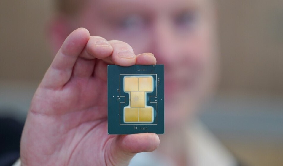
Intel Realizes the Only Way to Save x86 is to Democratize it, Reopens x86 IP Licensing

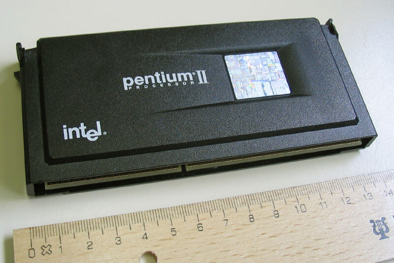
Back in the glory days of x86 in the 1990s, you could buy an IBM PC-compatible x86 processor from not just Intel and AMD, but also the likes of Cyrix, IDT, Transmeta, and NEC. Competition among the various x86 licensees propelled innovation through the first half of the 32-bit era, but toward the end of the century, and with the Y2K frenzy looming, the PC processor market saw a slew of consolidations, such as Cyrix and IDT (later Centaur) being acquired by VIA Technology. As of 2000, only two companies made high performance x86 processors, and processors for servers—Intel and AMD, with VIA Technology limiting itself to the entry-level PC market. Then came along Arm Cortex 32-bit, graduating from the embedded computing market to client computing, driven by smartphones.

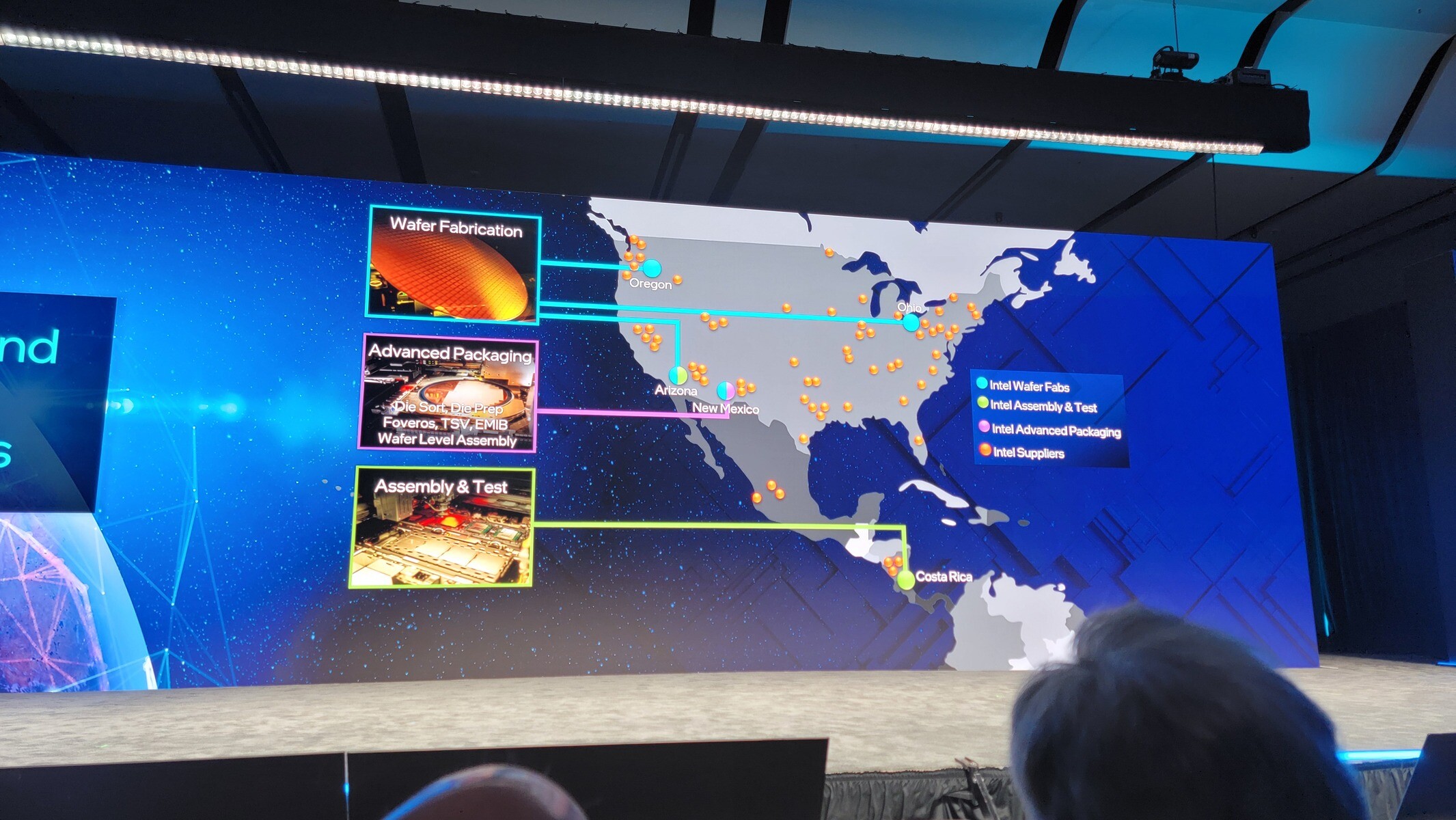
Intel's main competitor today isn't AMD, it's Arm and its constellation of licensees, such as Apple, Qualcomm, Samsung, MediaTek, and NVIDIA. Over the decades that followed the advent of the iPhone, Arm graduated from smartphones to PCs (eg: Snapdragon X, Apple M3), and servers (eg: Ampere Altra and NVIDIA Grace). Intel seems to have had the sudden realization that Intel Products should open up in the same way as Intel Foundry Services, and that just as IFS in Pat Gelsinger's words aspires to be the "TSMC of America," x86 should aspire to be the "Arm of America." The only way to go about doing this is to adopt an IP licensing model similar to that of Arm, where third parties are licensed the x86 machine architecture, and should pay Intel royalties based on their chip volumes, and other factors such as CPU core counts. Much like Arm, Intel could set up separate licensing models for SoC designers who want Intel's various IA cores as IP blocks, or just the x86 license to design their own cores, like AMD does. Since Intel is a founding member of the UCIe alliance, it could even offer up Compute tiles as chiplets.

Intel Redefines the Foundry for an Era of AI

Artificial intelligence isn't just driving headlines and stock valuations. It's also "pushing the boundaries of silicon technology, packaging technology, the construction of silicon, and the construction of racks and data centers," says Intel's Bob Brennan. "There is an insatiable demand," Brennan adds. Which is great timing since his job is to help satisfy that demand.

Brennan leads customer solutions engineering for Intel Foundry, which aims to make it as easy and fast as possible for the world's fabless chipmakers to fabricate and assemble their chips through Intel factories. "We are engaged from architecture to high-volume manufacturing—soup to nuts—and we present the customer with a complete solution," Brennan asserts.

Intel 10A (1 nm-class) Node to Enter Mass Production in 2027

Last week at the Intel Foundry Services Connect event, Intel unveiled its Intel 14A foundry node (1.4 nm-class), to succeed its Intel 18A and Intel 20A nodes, with mass production on this node expected to commence in 2026. It turns out that there is an even more advanced node Intel is working on, which it didn't announce last week, but which was part of an NDA presentation that the company forgot to lift. We're talking about the new Intel 10A node, a 1 nm-class silicon fabrication node that's a generation ahead of Intel 20A. The company says that it expects mass production on the node to begin toward the end of 2027. It is on the backs of these sub-2 nm class nodes, and the impending organizational changes that sees Intel Foundry Services become a more independent commercial entity, that Intel CEO Pat Gelsinger thinks that Intel will become the "TSMC of the West."

Currently, fabs that utilize EUV (extreme ultraviolet) lithography, namely the Intel 4, Intel 3, and Intel 20A; together make barely 15% of Intel's wafer volumes, with the bulk of the foundry's production focusing on the DUV based Intel 7. EUV-based nodes are expected to linearly grow till 2025, but what's interesting is that Intel doesn't see the kind of multi-year stagnation on Intel 4 and Intel 3 that it's currently experiencing with Intel 7; with wafer volumes of Intel 20A and 18A expected to exceed those of the Intel 4 and Intel 3 within 2025. By 2026, Intel expects that there will be twice as many Intel 20A/18A wafers pushed as Intel 4 and Intel 3. Although they use EUV, Intel 4 and Intel 3 are Intel's final nodes to implement FinFET transistors, as the company transitions to nanosheets with Intel 20A (which are called RibbonFETs in Intel jargon). Intel did not get into the technology behind Intel 10A. The company, along with Samsung and TSMC, demonstrated its stacked CFET transistor in 2023, which will power foundry nodes as nanosheets mature. Intel in its presentation also talked about the next wave of factory automation implemented by IFS, which sees AI-driven "cobots" (collaborative robots) replace humans for more roles in the clean room.

Intel to Make its Most Advanced Foundry Nodes Available even to AMD, NVIDIA, and Qualcomm

Intel CEO Pat Gelsinger, speaking at the Intel Foundry Services (IFS) Direct Connect event, confirmed to Tom's Hardware that he hopes to turn IFS into the West's premier foundry company, and a direct technological and volume rival to TSMC. He said that there is a clear line of distinction between Intel Products and Intel Foundry, and that later this year, IFS will be more legally distinct from Intel, becoming its own entity. The only way Gelsinger sees IFS being competitive to TSMC, is by making its most advanced semiconductor manufacturing nodes and 3D chip packaging innovations available to foundry customers other than itself (Intel Products), even if it means providing them to companies that directly compete with Intel products, such as AMD and Qualcomm.

Paul Alcorn of Tom's Hardware asked CEO Gelsinger "Intel will now offer its process nodes to some of its competitors, and there may be situations wherein your product teams are competing directly with competitors that are enabled by your crown jewels. How do you plan to navigate those types of situations and maybe soothe ruffled feathers on your product teams?" To this, Gelsinger responded "Well, if you go back to the picture I showed today, Paul, there are Intel products and Intel foundry, There's a clean line between those, and as I said on the last earnings call, we'll have a setup separate legal entity for Intel foundry this year," Gelsinger responded. "We'll start posting separate financials associated with that going forward. And the foundry team's objective is simple: Fill. The. Fabs. Deliver to the broadest set of customers on the planet."

Intel Foundry Services (IFS) and Cadence Design Systems Expand Partnership on SoC Design

Intel Foundry Services (IFS) and Cadence Design Systems Inc. today announced a multiyear strategic agreement to jointly develop a portfolio of key customized intellectual property (IP), optimized design flows and techniques for Intel 18A process technology featuring RibbonFET gate-all-around transistors and PowerVia backside power delivery. Joint customers of the companies will be able to accelerate system-on-chip (SoC) project schedules on process nodes from Intel 18A and beyond while optimizing for performance, power, area, bandwidth and latency for demanding artificial intelligence, high performance computing and premium mobile applications.

"We're very excited to expand our partnership with Cadence to grow the IP ecosystem for IFS and provide choice for customers," said Stuart Paann, Intel senior vice president and general manager of IFS. "We will leverage Cadence's world-class portfolio of leading IP and advanced design solutions to enable our customers to deliver high-volume, high-performance and power-efficient SoCs on Intel's leading-edge process technologies."

Report: Intel Seeks $2 Billion in Funding for Ireland Fab 34 Expansion

According to a Bloomberg report, Intel is seeking to raise at least $2 billion in equity funding from investors for expanding its fabrication facility in Leixlip, Ireland, known as Fab 34. The chipmaker has hired an advisor to find potential investors interested in providing capital for the project. Fab 34 is currently Intel's only chip plant in Europe that uses cutting-edge extreme ultraviolet (EUV) lithography. It produces processors on the Intel 4 process node, including compute tiles for Meteor Lake client CPUs and expected future Xeon data center chips. While $2 billion alone cannot finance the construction of an entirely new fab today, it can support meaningful expansion or upgrades of existing capacity. Intel likely aims to grow Fab 34's output and/or transition it to more advanced 3 nm-class technologies like Intel 3, Intel 20A, or Intel 18A.

Expanding production aligns with Intel's needs for its own products and its Intel Foundry Services business, providing contract manufacturing. Intel previously secured a $15 billion investment from Brookfield Infrastructure for its Arizona fabs in exchange for a 49% stake, demonstrating the company's willingness to partner to raise capital for manufacturing projects. The Brookfield deal also set a precedent of using outside financing to supplement Intel's own spending budget. It provided $15 billion in effectively free cash flow Intel can redirect to other priorities like new fabs without increasing debt. Intel's latest fundraising efforts for the Ireland site follow a similar equity investment model that leverages outside capital to support its manufacturing expansion plans. Acquiring High-NA EUV machinery for manufacturing is costly, as these machines can reach up to $380 million alone.

NVIDIA to Create AI Semi-custom Chip Business Unit

NVIDIA is reportedly working to set up a new business unit focused on designing semi-custom chips for some of its largest data-center customers, Reuters reports. NVIDIA dominates the AI HPC processor market, although even its biggest customers are having to shop from its general lineup of A100 series and H100 series HPC processors. There are reports of some of these customers venturing out of the NVIDIA fold, wanting to develop their own AI processor designs. It is to cater to exactly this segment that NVIDIA is setting up the new unit.

A semi-custom chip isn't just a bespoke chip designed to a customer's specifications. It is co-developed by NVIDIA and its customer, using mainly NVIDIA IP blocks, but also integrating some third-party IP blocks the customer may want; and more importantly, approach semiconductor fabrication companies such as TSMC, Samsung, or Intel Foundry Services as separate entities from NVIDIA for their wafer allocation. For example, a company like Google may have a certain amount of wafer pre-allocation with TSMC (eg: for its Tensor SoCs powering the Pixel smartphones), which it may want to tap into for a semi-custom AI HPC processor for its cloud business. NVIDIA assesses a $30 billion TAM for this specific business unit—that's all its current customers wanting to pursue their own AI processor projects, who will now be motivated to stick to NVIDIA.

TSMC Allegedly Not Rushing into Adoption of High-NA EUV Machinery

DigiTimes Asia has reached out to insiders at fabrication toolmakers in an effort to delve deeper into claims made by industry analysts at the start of 2024—both SemiAnalysis and China Renaissance have proposed that TSMC is unlikely to adopt High-NA EUV production techniques within a five year period. The latest news article explores a non-upgrade approach for the next couple of years: "TSMC has not placed orders for high-numerical aperture (High-NA) extreme ultraviolet (EUV) tools and is unlikely to use the technology in 2 nm and 1.4 nm (A14) process manufacturing." Intel Foundry Services (IFS) will be one of the first semiconductor manufacturers to go online with ASML's latest and greatest machinery, although no firm timeframes have been confirmed. Team Blue's Taiwanese rival (and occasional business partner) is seemingly happy with its existing infrastructure, but industry watchdogs propose that cost considerations are key factors behind TSMC's cautious planning for the next decade.

The DigiTimes insider sources believe that TSMC will not budge until at least 2029, possibly coinciding with a 1 nm production node—analysts at China Renaissance reckon that High-NA EUV machines could be delivered in the future when facilities are readied for an "A10" codenamed process. TSMC published a very ambitious "transistor count" product timeline in early January (see below)—the first "1 nm" products are supposedly targeted for a 2030 rollout, but this schedule could change due to unforeseen circumstances. Intel is expected to "phase in" its fanciest ASML gear collection once the 18A process becomes old hat—Tom's Hardware thinks that 2026 - 2027 is a feasible timeframe.

TSMC Overtakes Intel and Samsung to Become World's Largest Semiconductor Maker by Revenue

Taiwan Semiconductor Manufacturing Company (TSMC) has reached a significant milestone, overtaking Intel and Samsung to become the world's largest semiconductor maker by revenue. According to Taiwanese financial analyst Dan Nystedt, TSMC earned $69.3 billion in revenue in 2023, surpassing Intel's $63 billion and Samsung's $58 billion. This is a remarkable achievement for the Taiwanese chipmaker, which has historically lagged behind Intel and Samsung in terms of revenue despite being the world's largest semiconductor foundry. TSMC's meteoric rise has been fueled by the increased demand for everything digital - from PCs to game consoles - during the coronavirus pandemic in 2020, and AI demand in the previous year. With its cutting-edge production capabilities allowing it to manufacture chips using the latest process technologies, TSMC has pulled far ahead of Intel and Samsung and can now charge a premium for its services.

This is reflected in its financials. For the 6th straight quarter, TSMC's Q4 2023 revenue of $19.55 billion also beat Intel's $15.41 billion and Samsung's $16.42 billion chip division revenue. As the world continues its rapid transformation in the AI era of devices, TSMC looks set to hold on to its top position for the foreseeable future. Its revenue and profits will likely continue to eclipse those of historical giants like Intel and Samsung. However, a big contender is Intel Foundry Services, which is slowly starting to gain external customers. If IFS takes off and new customers start adopting Intel as their foundry of choice, team blue could regain leadership in the coming years.

Intel Foundry Services Get 18A Order: Arm-based 64-Core Neoverse SoC

Faraday Technology Corporation, a Taiwanese silicon IP designer, has announced plans to develop a new 64-core system-on-chip (SoC) utilizing Intel's most advanced 18A process technology. The Arm-based SoC will integrate Arm Neoverse compute subsystems (CSS) to deliver high performance and efficiency for data centers, infrastructure edge, and 5G networks. This collaboration brings together Faraday, Arm, and Intel Foundry Services. Faraday will leverage its ASIC design and IP solutions expertise to build the SoC. Arm will provide the Neoverse compute subsystem IP to enable scalable computing. Intel Foundry Services will manufacture the chip using its cutting-edge 18A process, which delivers one of the best-in-class transistor performance.

The new 64-core SoC will be a key component of Faraday's upcoming SoC evaluation platform. This platform aims to accelerate customer development of data center servers, high-performance computing ASICs, and custom SoCs. The platform will also incorporate interface IPs from the Arm Total Design ecosystem for complete implementation and verification. Both Arm and Intel Foundry Services expressed excitement about working with Faraday on this advanced Arm-based custom silicon project. "We're thrilled to see industry leaders like Faraday and Intel on the cutting edge of Arm-based custom silicon development," said an Arm spokesperson. Intel SVP Stuart Pann said, "We are pleased to work with Faraday in the development of the SoC based on Arm Neoverse CSS utilizing our most competitive Intel 18A process technology." The collaboration represents Faraday's strategic focus on leading-edge technologies to meet evolving application requirements. With its extensive silicon IP portfolio and design capabilities, Faraday wants to deliver innovative solutions and break into next-generation computing design.

Intel Reports Fourth-Quarter and Full-Year 2023 Financial Results

Intel Corporation today reported fourth-quarter and full-year 2023 financial results. "We delivered strong Q4 results, surpassing expectations for the fourth consecutive quarter with revenue at the higher end of our guidance," said Pat Gelsinger, Intel CEO. "The quarter capped a year of tremendous progress on Intel's transformation, where we consistently drove execution and accelerated innovation, resulting in strong customer momentum for our products. In 2024, we remain relentlessly focused on achieving process and product leadership, continuing to build our external foundry business and at-scale global manufacturing, and executing our mission to bring AI everywhere as we drive long-term value for stakeholders."

David Zinsner, Intel CFO, said, "We continued to drive operational efficiencies in the fourth quarter, and comfortably achieved our commitment to deliver $3 billion in cost savings in 2023. We expect to unlock further efficiencies in 2024 and beyond as we implement our new internal foundry model, which is designed to drive greater transparency and accountability and higher returns on our owners' capital." For the full year, the company generated $11.5 billion in cash from operations and paid dividends of $3.1 billion.

Intel and UMC Announce New Foundry Collaboration

Intel Corp. and United Microelectronics Corporation ("UMC"), a leading global semiconductor foundry, today announced that they will collaborate on the development of a 12-nanometer semiconductor process platform to address high-growth markets such as mobile, communication infrastructure and networking. The long-term agreement brings together Intel's at-scale U.S. manufacturing capacity and UMC's extensive foundry experience on mature nodes to enable an expanded process portfolio. It also offers global customers greater choice in their sourcing decisions with access to a more geographically diversified and resilient supply chain.

"Taiwan has been a critical part of the Asian and global semiconductor and broader technology ecosystem for decades, and Intel is committed to collaborating with innovative companies in Taiwan, such as UMC, to help better serve global customers," said Stuart Pann, Intel senior vice president and general manager of Intel Foundry Services (IFS). "Intel's strategic collaboration with UMC further demonstrates our commitment to delivering technology and manufacturing innovation across the global semiconductor supply chain and is another important step toward our goal of becoming the world's second-largest foundry by 2030."

Intel, TSMC, and Samsung, Demo CFETs at IEEE IEDM Conference, Near Doubling in Transistor Densities in Sight

Last week at the IEEE International Electron Devices Meeting, the world's top-three semiconductor foundries, TSMC, Intel (Intel Foundry Services or IFS), and Samsung Electronics, demonstrated their respective approaches to an evolutionary new transistor device called the CFET, or complementary field-effect transistors. A CFET is a kind of 3-D transistor that stacks both kinds of FETs needed for CMOS logic. All three fabs are transitioning from FinFET to nanosheets, or GAAFETs (gates all-around FETs).

While FinFETs use vertical silicon fins, with gates controlling the flow of current through them; while in a nanosheet, the vertical fin is cut into a set of ribbons, each surrounded by the gate. A CFET is essentially a taller nanosheet device in which uses half of the available ribbons for one device, and the other half for another. This device builds the two types of transistor, nFETs and pFETs on top of each other, in an integrated process. CFETs are the evolutionary next step to conventional GAAFETs, and it's predicted to enter mass production only 7-10 years from now. By that time, the industry will begin to feel the pushback from technological barriers preventing development beyond 10 angstrom-class nodes.

NVIDIA CFO Hints at Intel Foundry Services Partnership

NVIDIA CFO Colette Kress, responding to a question in the Q&A session of the recent UBS Global Technology Conference, hinted at the possibility of NVIDIA onboarding a third semiconductor foundry partner besides its current TSMC and Samsung, with the implication being Intel Foundry Services (IFS). "We would love a third one. And that takes a work of what are they interested in terms of the services. Keep in mind, there is other ones that may come to the U.S. TSMC in the U.S. may be an option for us as well. Not necessarily different, but again in terms of the different region. Nothing that stops us from potentially adding another foundry."

NVIDIA currently sources its chips from TSMC and Samsung. It uses the premier Taiwanese fab for its latest "Ada" GPUs and "Hopper" AI processors, while using Samsung for its older generation "Ampere" GPUs. The addition of IFS as a third foundry partner could improve the company's supply-chain resilience in an uncertain geopolitical environment; given that IFS fabs are predominantly based in the US and the EU.

Ericsson First to Market with Processors Made on "Intel 4" Technology

Ericsson, a massive player in networking and cellular technology, has announced their new lineup of RAN Compute (Radio Access Network) processors as well as new high bandwidth routers built around in-house silicon designs fabbed on Intel 4, beating Intel's own Meteor Lake processors to market. These new processors are not something the average person is going to be using in their PCs or home routers, but they are pivotal in the reliability and speed of current and future generation 5G networking as the devices they power handle the ever increasing traffic and bandwidth demands of modern networks. In its press release Ericsson notes that the new RAN Processor 6672 and Radio Processor 6372 offer four times more capacity at twice the efficiency compared to their previous generation. They claim that the power draw of their new processors on Intel 4 is between 30% and 60% lower than the industry benchmarks.

Ericsson signed on as one of Intel's largest customers when Intel announced their "Intel Foundry Services" initiative under the IDM 2.0 strategy to offer chip designers the ability to fab their processors at Intel fabs. The strategy has - at least outwardly - appeared to be a boon to Intel as they've signed on large partnerships ranging from big budget defense contractors to datacenter clientele and even ARM. The new RAN Compute systems from Ericsson packed full of technology built on "Intel 4" even ahead of Intel's own designs exemplifies that Intel is at the very least committed to the strategy, and Ericsson has already announced plans for even more chips on Intel's "18A" process slated for 2025.

Intel Lunar Lake-MX SoC with On-Package LPDDR5X Memory Detailed

With the reality of high performance Arm processors from Apple and Qualcomm threatening Intel's market share in the client computing space, Intel is working on learner more PCB-efficient client SoCs that can take the fight to them, while holding onto the foundations of x86. The first such form-factor of processors are dubbed -MX. These are essentially -U segment processors with memory on package, to minimize PCB footprint. Intel has fully integrated the PCH into the processor chip with "Meteor Lake," with PCH functions scattered across the SoC and I/O tiles of the processor. An SoC package with dimensions similar to those of -UP4 packages meant for ultrabooks, can now cram main memory, so the PCBs of next-generation notebooks can be further compacted.

Intel had recently shown Meteor Lake-MX packages to the press as a packaging technology demonstration in its Arizona facility. It's unclear whether this could release as actual products, but in a leaked company presentation, confirmed that its first commercial outing will be with Lunar Lake-MX. The current "Alder Lake-UP4" package measures 19 mm x 28.5 mm, and is a classic multi-chip module that combines a monolithic "Alder Lake" SoC die with a PCH die. The "Meteor Lake-UP4" package measures 19 mm x 23 mm, and is a chiplet-based processor, with a Foveros base tile that holds the Compute (CPU cores), Graphics (iGPU), SoC and I/O (platform core-logic) tiles. The "Lunar Lake-MX" package is slightly larger than its -UP4 predecessors, measuring 27 mm x 27.5 mm, but completely frees up space on the PCB for memory.

Intel Announces Intent to Operate Programmable Solutions Group as Standalone Business Under Leadership of Sandra Rivera

Intel Corporation today announced its intent to separate its Programmable Solutions Group (PSG) operations into a standalone business. This will give PSG the autonomy and flexibility it needs to fully accelerate its growth and more effectively compete in the FPGA industry, which serves a broad array of markets, including the data center, communications, industrial, automotive, aerospace and defense sectors. Intel also announced that Sandra Rivera, executive vice president at Intel, will assume leadership of PSG as chief executive officer; Shannon Poulin has been named chief operating officer.

Standalone operations for PSG are expected to begin Jan. 1, 2024, with ongoing support from Intel. Intel expects to report PSG as a separate business unit when it releases first-quarter 2024 financials. Over the next two to three years, Intel intends to conduct an IPO for PSG and may explore opportunities with private investors to accelerate the business's growth, with Intel retaining a majority stake.

Intel to Start High-Volume EUV Production in Ireland, Intel 4 Node Enters Mass-production

Intel Foundry Services (IFS) today announced that it will commence mass-production on its first silicon fabrication node that leverages extreme ultraviolet (EUV) lithography, Intel 4. On September 29, the Intel 4 node will start rolling at the company's facility in Leixlip, Ireland, dubbed Fab 34. CEO Pat Gelsinger, Dr. Ann Kelleher, general manager of Technology Development at Intel, and Keyvan Esfarjani, chief global operations officer, will be present at a ceremony commemorating production of the first wafers.

Intel 4 is an advanced foundry that leverages EUV, and offers both transistor densities and electrical characteristics comparable to TSMC's 5 nm-class and 4 nm-class foundry nodes. Among the first chips to be built are the compute tiles of the company's Core "Meteor Lake" processors, which contain their next-generation CPU cores. Compared to the current Intel 7 node, Intel 4 offers double the area scaling for logic libraries, a 20% iso-power improvement, and introduces the new metal-insulator-metal (MIM) capacitor.

Intel Foundry Services and Tower Semiconductor Announce New US Foundry Agreement

Intel Foundry Services (IFS) and Tower Semiconductor, a leading foundry for analog semiconductor solutions, today announced an agreement where Intel will provide foundry services and 300 mm manufacturing capacity to help Tower serve its customers globally. Under the agreement, Tower will utilize Intel's advanced manufacturing facility in New Mexico. Tower will invest up to $300 million to acquire and own equipment and other fixed assets to be installed in the New Mexico facility, providing a new capacity corridor of over 600,000 photo layers per month for Tower's future growth, enabling capacity to support forecasted customer demand for 300 mm advanced analog processing.

This agreement demonstrates the commitment from both Intel and Tower to expand their respective foundry footprints with unparalleled solutions and scaled capabilities. Intel will manufacture Tower's highly differentiated 65-nanometer power management BCD (bipolar-CMOS-DMOS) flows, among other flows at Intel's Fab 11X in Rio Rancho, New Mexico.

Intel Cancels Tower Semiconductor Merger

Intel Corporation (Nasdaq: INTC) today announced that it has mutually agreed with Tower Semiconductor (Nasdaq: TSEM) to terminate its previously disclosed agreement to acquire Tower due to the inability to obtain in a timely manner the regulatory approvals required under the merger agreement, dated Feb. 15, 2022. In accordance with the terms of the merger agreement and in connection with its termination, Intel will pay a termination fee of $353 million to Tower.

"Our foundry efforts are critical to unlocking the full potential of IDM 2.0, and we continue to drive forward on all facets of our strategy," said Pat Gelsinger, CEO of Intel. "We are executing well on our roadmap to regain transistor performance and power performance leadership by 2025, building momentum with customers and the broader ecosystem and investing to deliver the geographically diverse and resilient manufacturing footprint the world needs. Our respect for Tower has only grown through this process, and we will continue to look for opportunities to work together in the future."

Intel and Synopsys Expand Partnership to Enable Leading IP on Intel Advanced Process Nodes

Intel and Synopsys announced that they have entered into a definitive agreement to expand the companies' long-standing IP (intellectual property) and EDA (electronic design automation) strategic partnership with the development of a portfolio of IP on Intel 3 and Intel 18A for Intel's foundry customers. The availability of key IP on Intel advanced process nodes will create a more robust offering for new and existing Intel Foundry Services (IFS) customers.

"Marking another important step in our IDM 2.0 strategy, this transaction will foster a vibrant foundry ecosystem by allowing designers to fully realize the advantages of Intel 3 and Intel 18A process technologies and quickly bring differentiated products to market," said Stuart Pann, senior vice president and general manager of IFS. "Synopsys brings a strong track record of delivering high-quality IP to a broad customer base, and this agreement will help accelerate the availability of IP on advanced IFS nodes for mutual customers."

RAMP-C Program on Intel 18A Adds 2 Strategic Defense Industrial Base Customers

Intel Foundry Services is onboarding two new defense industrial base (DIB) customers, Boeing and Northrop Grumman, as part of phase two of the U.S. Department of Defense (DoD)'s Rapid Assured Microelectronics Prototypes - Commercial (RAMP-C) program. In phase two of the RAMP-C program, customers will use Intel 18A process technology and industry-standard electrical design and analysis tools and intellectual property (IP) to develop, tape-out and fabricate test chips in preparation for product design tape-outs.

"We are pleased to welcome Boeing and Northrop Grumman to the RAMP-C program. Boeing and Northrop Grumman will use their industry expertise to develop and support leading-edge semiconductor solutions using Intel 18A process technology for the success of vital DoD and national security systems. Together, we will continue to bolster the domestic semiconductor supply chain and ensure that the United States maintains leadership in process technology R&D, advanced manufacturing and microelectronics systems," said Kapil Wadhera, vice president of Intel Foundry Services and general manager of Foundry Solutions Business Group.

Samsung Claims Higher 3 nm Yields than TSMC

Competition between Samsung and TSMC in the 4 nm and 3 nm foundry process markets is about to heat up, with the Korean foundry claiming yields competitive to those of TSMC, according to a report in the Kukmin Ilbo, a Korean daily newspaper. 4 nm is the final silicon fabrication process to use the FinFET technology that powered nodes ranging between 16 nm to 4 nm. Samsung Foundry is claiming 4 nm wafer yields of 75%, against the 80% yields figure put out by TSMC. 4 nm powers several current-generation mobile SoCs, PC processors, and more importantly, the GPUs driving the AI gold-rush.

Things get very interesting with 3 nm, the node that debuts GAA-FET (gates all around FET) technology. Here, Samsung claims to offer higher yields than TSMC, with its 3 nm GAA node clocking 60% yields, against 55% put out by TSMC. Samsung was recently bitten by a scandal where its engineers allegedly falsified yields figures to customers to score orders, which had a cascading effect on the volumes and competitiveness of their customers. We're inclined to think that Samsung has taken lessons and is more careful with the yields figures being reported in the press. Meanwhile, Intel Foundry Services competes with the Intel 3 node, which is physically 7 nm FinFET, but with electrical characteristics comparable to those of 3 nm.

Intel Expects to Beat TSMC at 2nm, Intel Foundry to Operate Almost as a Separate Business

Intel's integrated device manufacturing (IDM) has been experiencing a lot of trouble in recent years, and the company is not a leading-edge semiconductor manufacturer, with TSMC taking the pole position. However, the new restructuring hopes to change some of the business operations to increase its efficiency and establish Intel as the go-to foundry for customers. David Zinsner, Executive Vice President and the Chief Financial Officer, alongside Jason Grebe, Corporate Vice President & GM of the Corporate Planning Group at Intel, joined investors to explain how IDM will transform into a next-generation business. Intel IDM, including Intel Foundry Services (IFS), will get a new operation model, which will put IDM as an almost separate business unit with its own profit and loss (P&L) statement published in the quarterly/yearly financial report.

According to Intel, the company's IDM 1.0 strategy has been serving it well, but IDM 2.0 is needed to build next-generation nodes as the capital required for them is massive. Intel hopes to regain node leadership with the Intel 18A node in 2025. The company's strategy is still to have IFS as the second biggest external foundry business, presumably just behind TSMC. Putting IDM into its own P&L will result in $8-10 billion in "cost reduction opportunities, " including ramp rates, test time, and sort times based on the market pricing, not Intel's pricing. At the start, IDM is expected o start with a negative operating margin. Intel also states that keeping IFS as a business unit allows the company to simultaneously develop products on it and de-risk it for customers who want to build on IFS. The company is developing five different products (assuming packaging) on Intel 18A, all of which will be available for customers to use as well.

Intel, German Government Agree on Increased Scope for Wafer Fabrication Site in Magdeburg

Intel and the German federal government have signed a revised letter of intent for Intel's planned leading-edge wafer fabrication site in Magdeburg, the capital of Saxony-Anhalt state in Germany. The agreement encompasses Intel's expanded investment in the site, now expected to be more than 30 billion euros for two first-of-a-kind semiconductor facilities (also known as "fabs") in Europe, along with increased government support that includes incentives, reflecting the expanded scope and change in economic conditions since the site was first announced.

Intel acquired the land for the project in November 2022, and the first facility is expected to enter production in four to five years following the European Commission's approval of the incentive package. Given the current timeline and scale of the investment, Intel plans to deploy more advanced Angstrom-era technology in the facilities than originally envisioned. The Magdeburg site will serve Intel products and Intel Foundry Services customers.
Return to Keyword Browsing
Apr 30th, 2024 22:15 EDT change timezone

New Forum Posts

Popular Reviews

Controversial News Posts