News Posts matching #Intel 18A

Return to Keyword Browsing

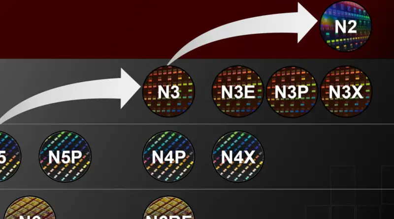
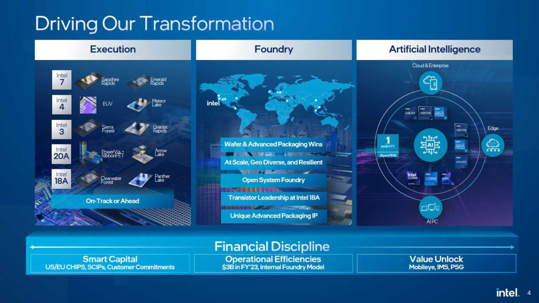
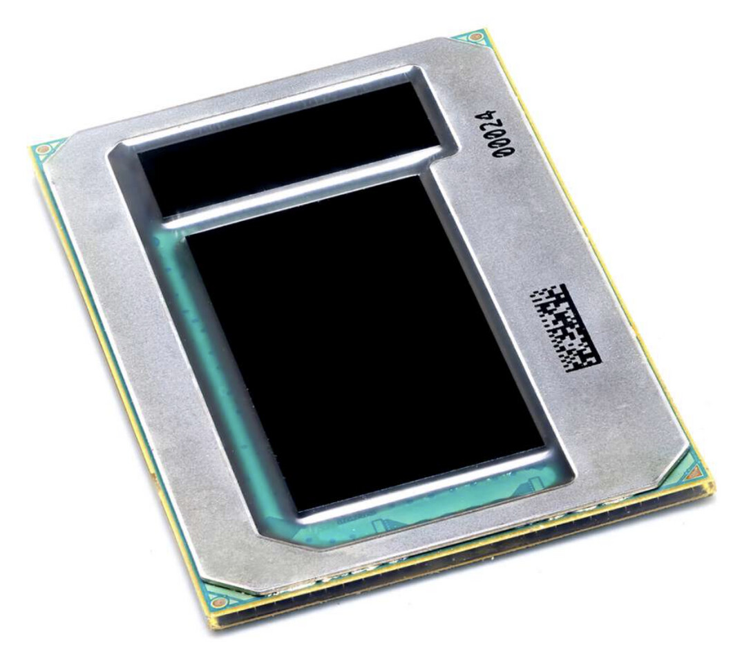
Intel Lunar Lake Chiplet Arrangement Sees Fewer Tiles—Compute and SoC

Intel Core Ultra "Lunar Lake-MX" will be the company's bulwark against Apple's M-series Pro and Max chips, designed to power the next crop of performance ultraportables. The MX codename extension denotes MoP (memory-on-package), which sees stacked LPDDR5X memory chips share the package's fiberglass substrate with the chip, to conserve PCB footprint, and give Intel greater control over the right kind of memory speed, timings, and power-management features suited to its microarchitecture. This is essentially what Apple does with its M-series SoCs powering its MacBooks and iPad Pros. Igor's Lab scored the motherlode on the way Intel has restructured the various components across its chiplets, and the various I/O wired to the package.

When compared to "Meteor Lake," the "Lunar Lake" microarchitecture sees a small amount of "re-aggregation" of the various logic-heavy components of the processor. On "Meteor Lake," the CPU cores and the iGPU sat on separate tiles—Compute tile and Graphics tile, respectively, with a large SoC tile sitting between them, and a smaller I/O tile that serves as an extension of the SoC tile. All four tiles sat on top of a Foveros base tile, which is essentially an interposer—a silicon die that facilitates high-density microscopic wiring between the various tiles that are placed on top of it. With "Lunar Lake," there are only two tiles—the Compute tile, and the SoC tile.

Intel and Arm Team Up to Power Startups

Intel and Arm have signed a memorandum of understanding that finalizes the Emerging Business Initiative, their collaboration to support the startup community. The initiative builds on the April 2023 multi-generation agreement to enable chip designers to build low-power compute system-on-chips (SoCs) on the Intel 18A process. Together, the companies will provide essential intellectual property (IP) and manufacturing support, while also making financial assistance available, to foster innovation and growth for startups developing a range of devices and servers built on Arm-based SoCs and manufactured by Intel Foundry. The Emerging Business Initiative was announced last month at Intel Foundry Direct Connect in San Jose, California.

"Intel Foundry and Arm share the belief that for technology to benefit everyone, the building blocks of innovation must be available to anyone. Startups play a crucial role in bringing the great promise of transformations like AI to reality. The Emerging Business Initiative provides a path for new companies to leverage leading-edge Arm-based SoCs and Intel Foundry's global manufacturing capabilities to make their ideas real," said Stuart Pann, Intel senior vice president and general manager of Foundry Services.

Intel Redefines the Foundry for an Era of AI

Artificial intelligence isn't just driving headlines and stock valuations. It's also "pushing the boundaries of silicon technology, packaging technology, the construction of silicon, and the construction of racks and data centers," says Intel's Bob Brennan. "There is an insatiable demand," Brennan adds. Which is great timing since his job is to help satisfy that demand.

Brennan leads customer solutions engineering for Intel Foundry, which aims to make it as easy and fast as possible for the world's fabless chipmakers to fabricate and assemble their chips through Intel factories. "We are engaged from architecture to high-volume manufacturing—soup to nuts—and we present the customer with a complete solution," Brennan asserts.

Cadence Digital and Custom/Analog Flows Certified for Latest Intel 18A Process Technology

Cadence's digital and custom/analog flows are certified on the Intel 18A process technology. Cadence design IP supports this node from Intel Foundry, and the corresponding process design kits (PDKs) are delivered to accelerate the development of a wide variety of low-power consumer, high-performance computing (HPC), AI and mobile computing designs. Customers can now begin using the production-ready Cadence design flows and design IP to achieve design goals and speed up time to market.

"Intel Foundry is very excited to expand our partnership with Cadence to enable key markets for the leading-edge Intel 18A process technology," said Rahul Goyal, Vice President and General Manager, Product and Design Ecosystem, Intel Foundry. "We will leverage Cadence's world-class portfolio of IP, AI design technologies, and advanced packaging solutions to enable high-volume, high-performance, and power-efficient SoCs in Intel Foundry's most advanced process technology. Cadence is an indispensable partner supporting our IDM2.0 strategy and the Intel Foundry ecosystem."

Intel Announces Intel 14A (1.4 nm) and Intel 3T Foundry Nodes, Launches World's First Systems Foundry Designed for the AI Era

Intel Corp. today launched Intel Foundry as a more sustainable systems foundry business designed for the AI era and announced an expanded process roadmap designed to establish leadership into the latter part of this decade. The company also highlighted customer momentum and support from ecosystem partners - including Synopsys, Cadence, Siemens and Ansys - who outlined their readiness to accelerate Intel Foundry customers' chip designs with tools, design flows and IP portfolios validated for Intel's advanced packaging and Intel 18A process technologies.

The announcements were made at Intel's first foundry event, Intel Foundry Direct Connect, where the company gathered customers, ecosystem companies and leaders from across the industry. Among the participants and speakers were U.S. Secretary of Commerce Gina Raimondo, Arm CEO Rene Haas, Microsoft CEO Satya Nadella, OpenAI CEO Sam Altman and others.

Intel Xeon "Clearwater Forest" CPUs Could Utilize Direct 3D Stacking Technology

Pat Gelsinger—CEO of Intel Corporation—happily revealed late last month, during an earnings call: "Clearwater Forest, our first Intel 18A part for servers has already gone into fab and Panther Lake for clients will be heading into Fab shortly." The former is positioned as the natural successor to Team Blue's many-times-delayed Xeon "Sierra Forest" (all E-Core) processor family. Intel's second generation E-core Xeon "Clearwater Forest" design is expected to launch in 2025, with a deployment of "Darkmont" efficiency-oriented cores. Official product roadmaps and patch notes have revealed basic "Clearwater Forest" information, but we have not seen many leaks. Bionic_Squash has a history of releasing strictly internal Intel presentation slides—Meteor Lake (MTL-S) desktop SKUs were uncovered last April.

Their latest discovery does not include any photo or documented evidence—Bionic_Squash's concise social media post stated: "Clearwater Forest uses 3D stacking with hybrid bonding." This claim points to the possible deployment of Foveros Direct advanced packaging—this technology was expected to be ready at some point within the second half of 2023, although a mid-December technology showcase implied that things were behind schedule. The fanciest "Clearwater Forest" Xeon processors could arrive with a maximum total of 288 E-core count (and 288 threads)—according to Wccftech analysis: "The CPU package is going to consist of a base tile on top of the interposer which is connected through a high-speed I/O, EMIB, and the cores will be sitting on the topmost layer...Foveros Direct technology will allow direct copper-to-copper bonding, enabling low resistance interconnects and around 10-micron bump pitches. Intel itself states that Foveros Direct will blur the boundary between where the wafer ends and the package begins."

Intel Foundry Services (IFS) and Cadence Design Systems Expand Partnership on SoC Design

Intel Foundry Services (IFS) and Cadence Design Systems Inc. today announced a multiyear strategic agreement to jointly develop a portfolio of key customized intellectual property (IP), optimized design flows and techniques for Intel 18A process technology featuring RibbonFET gate-all-around transistors and PowerVia backside power delivery. Joint customers of the companies will be able to accelerate system-on-chip (SoC) project schedules on process nodes from Intel 18A and beyond while optimizing for performance, power, area, bandwidth and latency for demanding artificial intelligence, high performance computing and premium mobile applications.

"We're very excited to expand our partnership with Cadence to grow the IP ecosystem for IFS and provide choice for customers," said Stuart Paann, Intel senior vice president and general manager of IFS. "We will leverage Cadence's world-class portfolio of leading IP and advanced design solutions to enable our customers to deliver high-volume, high-performance and power-efficient SoCs on Intel's leading-edge process technologies."

Report: Intel Seeks $2 Billion in Funding for Ireland Fab 34 Expansion

According to a Bloomberg report, Intel is seeking to raise at least $2 billion in equity funding from investors for expanding its fabrication facility in Leixlip, Ireland, known as Fab 34. The chipmaker has hired an advisor to find potential investors interested in providing capital for the project. Fab 34 is currently Intel's only chip plant in Europe that uses cutting-edge extreme ultraviolet (EUV) lithography. It produces processors on the Intel 4 process node, including compute tiles for Meteor Lake client CPUs and expected future Xeon data center chips. While $2 billion alone cannot finance the construction of an entirely new fab today, it can support meaningful expansion or upgrades of existing capacity. Intel likely aims to grow Fab 34's output and/or transition it to more advanced 3 nm-class technologies like Intel 3, Intel 20A, or Intel 18A.

Expanding production aligns with Intel's needs for its own products and its Intel Foundry Services business, providing contract manufacturing. Intel previously secured a $15 billion investment from Brookfield Infrastructure for its Arizona fabs in exchange for a 49% stake, demonstrating the company's willingness to partner to raise capital for manufacturing projects. The Brookfield deal also set a precedent of using outside financing to supplement Intel's own spending budget. It provided $15 billion in effectively free cash flow Intel can redirect to other priorities like new fabs without increasing debt. Intel's latest fundraising efforts for the Ireland site follow a similar equity investment model that leverages outside capital to support its manufacturing expansion plans. Acquiring High-NA EUV machinery for manufacturing is costly, as these machines can reach up to $380 million alone.

Samsung Lands Significant 2 nm AI Chip Order from Unnamed Hyperscaler

This week in its earnings call, Samsung announced that its foundry business has received a significant order for a two nanometer AI chips, marking a major win for its advanced fabrication technology. The unnamed customer has contracted Samsung to produce AI accelerators using its upcoming 2 nm process node, which promises significant gains in performance and efficiency over today's leading-edge chips. Along with the AI chips, the deal includes supporting HBM and advanced packaging - indicating a large-scale and complex project. Industry sources speculate the order may be from a major hyperscaler like Google, Microsoft, or Alibaba, who are aggressively expanding their AI capabilities. Competition for AI chip contracts has heated up as the field becomes crucial for data centers, autonomous vehicles, and other emerging applications. Samsung said demand recovery in 2023 across smartphones, PCs and enterprise hardware will fuel growth for its broader foundry business. It's forging ahead with 3 nm production while eyeing 2 nm for launch around 2025.

Compared to its 3 nm process, 2 nm aims to increase power efficiency by 25% and boost performance by 12% while reducing chip area by 5%. The new order provides validation for Samsung's billion-dollar investments in next-generation manufacturing. It also bolsters Samsung's position against Taiwan-based TSMC, which holds a large portion of the foundry market share. TSMC landed Apple as its first 2 nm customer, while Intel announced 5G infrastructure chip orders from Ericsson and Faraday Technology using its "Intel 18A" node. With rivals securing major customers, Samsung is aggressively pricing 2 nm to attract clients. Reports indicate Qualcomm may shift some flagship mobile chips to Samsung's foundry at the 2 nm node, so if the yields are good, the node has a great potential to attract customers.

Intel Foundry Services Get 18A Order: Arm-based 64-Core Neoverse SoC

Faraday Technology Corporation, a Taiwanese silicon IP designer, has announced plans to develop a new 64-core system-on-chip (SoC) utilizing Intel's most advanced 18A process technology. The Arm-based SoC will integrate Arm Neoverse compute subsystems (CSS) to deliver high performance and efficiency for data centers, infrastructure edge, and 5G networks. This collaboration brings together Faraday, Arm, and Intel Foundry Services. Faraday will leverage its ASIC design and IP solutions expertise to build the SoC. Arm will provide the Neoverse compute subsystem IP to enable scalable computing. Intel Foundry Services will manufacture the chip using its cutting-edge 18A process, which delivers one of the best-in-class transistor performance.

The new 64-core SoC will be a key component of Faraday's upcoming SoC evaluation platform. This platform aims to accelerate customer development of data center servers, high-performance computing ASICs, and custom SoCs. The platform will also incorporate interface IPs from the Arm Total Design ecosystem for complete implementation and verification. Both Arm and Intel Foundry Services expressed excitement about working with Faraday on this advanced Arm-based custom silicon project. "We're thrilled to see industry leaders like Faraday and Intel on the cutting edge of Arm-based custom silicon development," said an Arm spokesperson. Intel SVP Stuart Pann said, "We are pleased to work with Faraday in the development of the SoC based on Arm Neoverse CSS utilizing our most competitive Intel 18A process technology." The collaboration represents Faraday's strategic focus on leading-edge technologies to meet evolving application requirements. With its extensive silicon IP portfolio and design capabilities, Faraday wants to deliver innovative solutions and break into next-generation computing design.

Intel Reportedly Selects TSMC's 2 Nanometer Process for "Nova Lake" CPU Generation

A Taiwan Economic Daily news article proposes that a couple of high profile clients are considering TSMC's 2 nanometer process—Apple is widely believed to be the first customer to join the foundry's queue for cutting edge services. The report posits that Intel is also signed up on the Taiwanese firm's 2 nm reservation list—TSMC is expected to start production in 2025—insiders reckon that Team Blue's "Nova Lake" CPU family is the prime candidate here. Its CPU tile is alleged to utilize TSMC 2 nm node. Intel's recent "Core" processor roadmaps do not display any technologies beyond 2025—many believe that "Nova Lake" is pencilled in for a loose 2026 launch window, perhaps within the second half of the year.

The existence of "Nova Lake" was revealed late last year by HWiNFO patch notes—a short entry mentioned preliminary support for the family's integrated GPU. Intel is engaged in hyping up of its own foundry's 20A and 18A processes, but remain reliant on TSMC plants for various bits of silicon. Industry tipsters reckon that aspects of "Lunar Lake" CPUs are based on the Taiwanese foundry's N3B node. Team Blue Corporation and United Microelectronics Corporation (UMC) announced a new development partnership last week, but initial offerings will arrive on a relatively passé "12-nanometer semiconductor process platform." TSMC's very advanced foundry services seem to be unmatched at this juncture.

Intel "Panther Lake" Targets Substantial AI Performance Leap in 2025

Pat Gelsinger, CEO of Intel Corporation, has outlined future performance expectations for the company's Core range of processors. In a recent fourth quarter 2023 earnings call he declared: "The Core Ultra platform delivers leadership AI performance today with our next-generation platforms launching later this year, Lunar Lake and Arrow Lake tripling our AI performance. In 2025 with Panther Lake, we will grow AI performance up to an additional 2x." Team Blue's Intel Core Ultra "Meteor Lake" mobile processors arrived right at the tail end of last year, as a somewhat delayed answer to AMD's Ryzen 7040 "Phoenix" APU series—both leveraging their own AI-crunching NPU technologies. Gelsinger believes that the launch of Lunar Lake and Arrow Lake Core product lines will bring significant (3x) AI processing improvements over Meteor Lake. He seemed to confident in a delay-free release schedule for the new year and beyond: "We are first in the industry to have incorporated both gate-all-around and backside power delivery in a single process node, the latter unexpected two years ahead of our competition. Arrow Lake, our lead Intel 20A vehicle will launch this year."

He proceeded to gush about their next node advancement: "Intel 18A is expected to achieve manufacturing readiness in second half 2024, completing our five nodes in four year journey and bringing us back to process leadership. I am pleased to say that Clearwater Forest, our first Intel 18A part for servers has already gone into fab and Panther Lake for clients will be heading into Fab shortly." Industry experts posit that Core "Panther Lake" parts could borrow elements from the next generation Xeon "Clearwater Forest" efficiency-focused family—possibly the latter's "Darkmont" E-cores, to accompany "Cougar Cove" P-cores. The Intel CEO is quite excited about the manufacturing outlay for 2025: "I'll just say, hey, we look at this every single day and we're scrutinizing carefully our progress on 18A. And obviously the great news that we just described those Clearwater Forest taping out, that gives us a lot of confidence that 18A is healthy. That's a major product for us. Panther Lake following that shortly."

Intel Reports Fourth-Quarter and Full-Year 2023 Financial Results

Intel Corporation today reported fourth-quarter and full-year 2023 financial results. "We delivered strong Q4 results, surpassing expectations for the fourth consecutive quarter with revenue at the higher end of our guidance," said Pat Gelsinger, Intel CEO. "The quarter capped a year of tremendous progress on Intel's transformation, where we consistently drove execution and accelerated innovation, resulting in strong customer momentum for our products. In 2024, we remain relentlessly focused on achieving process and product leadership, continuing to build our external foundry business and at-scale global manufacturing, and executing our mission to bring AI everywhere as we drive long-term value for stakeholders."

David Zinsner, Intel CFO, said, "We continued to drive operational efficiencies in the fourth quarter, and comfortably achieved our commitment to deliver $3 billion in cost savings in 2023. We expect to unlock further efficiencies in 2024 and beyond as we implement our new internal foundry model, which is designed to drive greater transparency and accountability and higher returns on our owners' capital." For the full year, the company generated $11.5 billion in cash from operations and paid dividends of $3.1 billion.

Intel Lunar Lake-MX SoC with On-Package LPDDR5X Memory Detailed

With the reality of high performance Arm processors from Apple and Qualcomm threatening Intel's market share in the client computing space, Intel is working on learner more PCB-efficient client SoCs that can take the fight to them, while holding onto the foundations of x86. The first such form-factor of processors are dubbed -MX. These are essentially -U segment processors with memory on package, to minimize PCB footprint. Intel has fully integrated the PCH into the processor chip with "Meteor Lake," with PCH functions scattered across the SoC and I/O tiles of the processor. An SoC package with dimensions similar to those of -UP4 packages meant for ultrabooks, can now cram main memory, so the PCBs of next-generation notebooks can be further compacted.

Intel had recently shown Meteor Lake-MX packages to the press as a packaging technology demonstration in its Arizona facility. It's unclear whether this could release as actual products, but in a leaked company presentation, confirmed that its first commercial outing will be with Lunar Lake-MX. The current "Alder Lake-UP4" package measures 19 mm x 28.5 mm, and is a classic multi-chip module that combines a monolithic "Alder Lake" SoC die with a PCH die. The "Meteor Lake-UP4" package measures 19 mm x 23 mm, and is a chiplet-based processor, with a Foveros base tile that holds the Compute (CPU cores), Graphics (iGPU), SoC and I/O (platform core-logic) tiles. The "Lunar Lake-MX" package is slightly larger than its -UP4 predecessors, measuring 27 mm x 27.5 mm, but completely frees up space on the PCB for memory.

Intel Reports Third-Quarter 2023 Financial Results

Intel Corporation today reported third-quarter 2023 financial results. "We delivered a standout third quarter, underscored by across-the-board progress on our process and product roadmaps, agreements with new foundry customers, and momentum as we bring AI everywhere," said Pat Gelsinger, Intel CEO. "We continue to make meaningful progress on our IDM 2.0 transformation by relentlessly advancing our strategy, rebuilding our execution engine and delivering on our commitments to our customers."

David Zinsner, Intel CFO, said, "Our results exceeded expectations for the third consecutive quarter, with revenue above the high end of our guidance and EPS benefiting from strong operating leverage and expense discipline. As demonstrated by our recent portfolio actions, we are highly focused on being great allocators of our owners' capital and unlocking value for shareholders."

Intel's Arizona Expansion Marks Construction Milestone

Marking a milestone in Intel's ongoing manufacturing expansion in Arizona, the company today announced that the initial portion of the cleanroom is "weather tight" and the "blow down" phase has begun at the company's two new leading-edge chip factories on its Ocotillo campus in Chandler, Arizona. This milestone underscores Intel's dedication to advancing its presence in the state and fostering technological innovation.

"Our commitment to Arizona runs deep, and as we expand our operations, we remain dedicated to addressing the growing demand for semiconductors and helping the United States regain its leadership position in this vital industry. This milestone represents the result of great teamwork, proficient teams and exceptional craftsmanship of the tradespeople, and it's thanks to their hard work that we've made such significant progress on our site while keeping our culture of caring and the safety of all as our top priority." -Dan Doron, Intel vice president and general manager of Fab Construction Enterprise

Intel Demoes Core "Lunar Lake" Processor from Two Generations Ahead

Intel at the 2023 InnovatiON event surprised audiences with a live demo of a reference notebook powered by a Core "Lunar Lake" processor. What's surprising about this is that "Lunar Lake" won't come out until 2025 (at least), and succeeds not just the upcoming "Meteor Lake" architecture, but also its succeeding "Arrow Lake," which debuts in 2024. Intel is expected to debut "Meteor Lake" some time later this year. What's also surprising is that Intel has proven that the Intel 18A foundry node works. The Compute tile of "Lunar Lake" is expected to be based on Intel 18A, which is four generations ahead of the current Intel 7, which will be succeeded by Intel 4, Intel 3, and Intel 20A along the way.

The demo focused on the generative AI capabilities of Intel's third generation NPU, the hardware backend of AI Boost. Using a local session of a tool similar to Stable Diffusion, the processor was made to generate the image of a giraffe wearing a hat; and a GPT program was made to pen the lyrics of a song in the genre of Taylor Swift from scratch. Both tasks were completed on stage using the chip's NPU, and in timeframes you'd normally expect from discrete AI accelerators or cloud-based services.

Intel Unveils Industry-Leading Glass Substrates to Meet Demand for More Powerful Compute

What's New: Intel today announced one of the industry's first glass substrates for next-generation advanced packaging, planned for the latter part of this decade. This breakthrough achievement will enable the continued scaling of transistors in a package and advance Moore's Law to deliver data-centric applications.

"After a decade of research, Intel has achieved industry-leading glass substrates for advanced packaging. We look forward to delivering these cutting-edge technologies that will benefit our key players and foundry customers for decades to come."
-Babak Sabi, Intel senior vice president and general manager of Assembly and Test Development

Intel Foundry Services and Tower Semiconductor Announce New US Foundry Agreement

Intel Foundry Services (IFS) and Tower Semiconductor, a leading foundry for analog semiconductor solutions, today announced an agreement where Intel will provide foundry services and 300 mm manufacturing capacity to help Tower serve its customers globally. Under the agreement, Tower will utilize Intel's advanced manufacturing facility in New Mexico. Tower will invest up to $300 million to acquire and own equipment and other fixed assets to be installed in the New Mexico facility, providing a new capacity corridor of over 600,000 photo layers per month for Tower's future growth, enabling capacity to support forecasted customer demand for 300 mm advanced analog processing.

This agreement demonstrates the commitment from both Intel and Tower to expand their respective foundry footprints with unparalleled solutions and scaled capabilities. Intel will manufacture Tower's highly differentiated 65-nanometer power management BCD (bipolar-CMOS-DMOS) flows, among other flows at Intel's Fab 11X in Rio Rancho, New Mexico.

Intel Cancels Tower Semiconductor Merger

Intel Corporation (Nasdaq: INTC) today announced that it has mutually agreed with Tower Semiconductor (Nasdaq: TSEM) to terminate its previously disclosed agreement to acquire Tower due to the inability to obtain in a timely manner the regulatory approvals required under the merger agreement, dated Feb. 15, 2022. In accordance with the terms of the merger agreement and in connection with its termination, Intel will pay a termination fee of $353 million to Tower.

"Our foundry efforts are critical to unlocking the full potential of IDM 2.0, and we continue to drive forward on all facets of our strategy," said Pat Gelsinger, CEO of Intel. "We are executing well on our roadmap to regain transistor performance and power performance leadership by 2025, building momentum with customers and the broader ecosystem and investing to deliver the geographically diverse and resilient manufacturing footprint the world needs. Our respect for Tower has only grown through this process, and we will continue to look for opportunities to work together in the future."

Intel and Synopsys Expand Partnership to Enable Leading IP on Intel Advanced Process Nodes

Intel and Synopsys announced that they have entered into a definitive agreement to expand the companies' long-standing IP (intellectual property) and EDA (electronic design automation) strategic partnership with the development of a portfolio of IP on Intel 3 and Intel 18A for Intel's foundry customers. The availability of key IP on Intel advanced process nodes will create a more robust offering for new and existing Intel Foundry Services (IFS) customers.

"Marking another important step in our IDM 2.0 strategy, this transaction will foster a vibrant foundry ecosystem by allowing designers to fully realize the advantages of Intel 3 and Intel 18A process technologies and quickly bring differentiated products to market," said Stuart Pann, senior vice president and general manager of IFS. "Synopsys brings a strong track record of delivering high-quality IP to a broad customer base, and this agreement will help accelerate the availability of IP on advanced IFS nodes for mutual customers."

Intel Reports Second-Quarter 2023 Financial Results, Foundry Services Business up

Intel Corporation today reported second-quarter 2023 financial results. "Our Q2 results exceeded the high end of our guidance as we continue to execute on our strategic priorities, including building momentum with our foundry business and delivering on our product and process roadmaps," said Pat Gelsinger, Intel CEO. "We are also well-positioned to capitalize on the significant growth across the AI continuum by championing an open ecosystem and silicon solutions that optimize performance, cost and security to democratize AI from cloud to enterprise, edge and client."

David Zinsner, Intel CFO, said, "Strong execution, including progress towards our $3 billion in cost savings in 2023, contributed to the upside in the quarter. We remain focused on operational efficiencies and our Smart Capital strategy to support sustainable growth and financial discipline as we improve our margins and cash generation and drive shareholder value." In the second quarter, the company generated $2.8 billion in cash from operations and paid dividends of $0.5 billion.

RAMP-C Program on Intel 18A Adds 2 Strategic Defense Industrial Base Customers

Intel Foundry Services is onboarding two new defense industrial base (DIB) customers, Boeing and Northrop Grumman, as part of phase two of the U.S. Department of Defense (DoD)'s Rapid Assured Microelectronics Prototypes - Commercial (RAMP-C) program. In phase two of the RAMP-C program, customers will use Intel 18A process technology and industry-standard electrical design and analysis tools and intellectual property (IP) to develop, tape-out and fabricate test chips in preparation for product design tape-outs.

"We are pleased to welcome Boeing and Northrop Grumman to the RAMP-C program. Boeing and Northrop Grumman will use their industry expertise to develop and support leading-edge semiconductor solutions using Intel 18A process technology for the success of vital DoD and national security systems. Together, we will continue to bolster the domestic semiconductor supply chain and ensure that the United States maintains leadership in process technology R&D, advanced manufacturing and microelectronics systems," said Kapil Wadhera, vice president of Intel Foundry Services and general manager of Foundry Solutions Business Group.

Report Suggests Intel Considering Investment in Arm's Upcoming IPO

Reuters has been informed this week by a trusted insider source that the higher-ups at Intel Corporation are holding talks with Japan's SoftBank about becoming a possible anchor investor in the latter's initial public offering (IPO) of Arm. The British semiconductor and software design company was wholly acquired by the Japanese multinational investment holding firm in 2016. This was followed by a failed takeover bid by NVIDIA—six years later. Arm is aiming to sell its shares via Nasdaq in Q3 or Q4 2023, with a goal of raising around $8 - $10 billion. It also formulated plans to adjust pricing models earlier this year, with news reports labelling the strategic act as an attempt to rake in more royalties.

Intel and Arm have already formed a relationship in recent times—thanks to the development of the former's low-power compute system-on-chips (SoCs). These are set to be built on Intel Foundry's 18A process. The two companies have signed a multi-generation agreement to collaborate on the design of a series of mobile chipsets as an opening product range—diversified options will follow in the future. Arm is rumored (according to Reuters) to be working on its own proprietary chip, but the deal with Intel allows it to use its partner's "open system foundry model."

With PowerVia, Intel Achieves a Chipmaking Breakthrough

Intel is about to turn chipmaking upside down with PowerVia, a new approach to delivering power that required a radical rethink to both how chips are made and how they are tested. For all the modern history of computer chips, they've been built like pizzas—from the bottom up, in layers. In the case of chips, you start with the tiniest features, the transistors, and then you build up increasingly less-tiny layers of wires that connect the transistors and different parts of the chip (these are called interconnects). Included among those top layers are the wires that bring in the power that makes the chip go.

When the chip is done, you flip it over, enclose it in packaging that provides connections to the outer world, and you're ready to put it in a computer. Unfortunately, this approach is running into problems. As they get smaller and denser, the layers that share interconnects and power connections have become an increasingly chaotic web that hinders the overall performance of each chip. Once an afterthought, "now they have a huge impact," says Ben Sell, vice president of Technology Development at Intel and part of the team that brought PowerVia to fruition. In short, power and signals fade, requiring workarounds or simply dumping more power in.
Return to Keyword Browsing
May 1st, 2024 05:44 EDT change timezone

New Forum Posts

Popular Reviews

Controversial News Posts