Thursday, July 2nd 2020

Kioxia Plans for Wafer-Level SSD

Wafer-scale design is getting popular it seems. Starting from the wafer-scale engine presented by Cerebras last year, which caused quite the shakeup in the industry, it seems that this design approach might be more useful than anyone thought. During VLSI Symposium 2020, Shigeo Oshima, Chief Engineer at Kioxia, had a presentation about new developments in SSD designs and implementations. What was one of the highlights of the presentation was the information that Kioxia is working on, was a technology Kioxia is referring to as wafer-level SSD.

The NAND chips used in SSDs would no longer be cut from the wafer and packaged separately. Instead, the wafer itself would represent the SSD. This is a similar approach Cerebras used with its wafer-scale engine AI processor. What would be gains of this approach compared to traditional methods of cutting up NAND chips and packaging them separately you might wonder? Well, for starters you wouldn't need to cut the wafer, package individual memory chips, and build the SSD out of them. Those steps could be skipped and there would be some cost savings present. And imagine if you decide to do wafer stacking. You could build super scaling SSDs with immense performance capable of millions of IOPS. However, for now, this is only a concept and it is just in early development. There is no possibility to find it in a final product anytime soon.
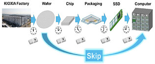
Kioxia Wafer-Level SSD
Source: Hardwareluxx.de
Add your own comment

15 Comments on Kioxia Plans for Wafer-Level SSD

#1
_JP_
So, if this comes to fruition*, do we start calling them Waffles or what?
"Hey Joe, did you fed the waffle to the server yet?"
"Nah, he's already full!"

*(not considering what solution they are going to come-up with to deliver for the controller, power delivery, power backup, bus/connectors and other regular stuff hot-swap storage solutions have had since the start)
Posted on Reply
#2
Chrispy_
That diagram is a bit disingenious. I mean, the big arrow implies that you just insert a round silicon wafer directly into a computer, which is obviously stupid and wrong. No motherboards exist that can accept raw wafers!

What I presume is happening is that a single die now represents the controller, the DRAM cache, and the voltage step-down circuitry, but it still needs to be packaged into a form-factor that can be plugged into a motherboard.
Posted on Reply
#3
Gungar
Chrispy_That diagram is a bit disingenious. I mean, the big arrow implies that you just insert a round silicon wafer directly into a computer, which is obviously stupid and wrong. No motherboards exist that can accept raw wafers!

What I presume is happening is that a single die now represents the controller, the DRAM cache, and the voltage step-down circuitry, but it still needs to be packaged into a form-factor that can be plugged into a motherboard.
Or maybe there is a reason why that department is no longer Toshiba...
Posted on Reply
#4
AnarchoPrimitiv
I'm a big storage nerd, so this story has be wondering a lot of things.... How would such an "SSD" interface with a computer? Would it use already existent protocol (e.g. NVMe? Perhaps over a PCIe 4.0/5.0/6.0x16) or would they develop a proprietary protocol? Would it interface with off the shelf x86 CPUs or would the build some standalone box with an FPGA or some customer Arm chip in it to act as a controller on steroids?

They should just glue it to Cerebras's wafer and just make it a gigantic L4 cache, haha
Posted on Reply
#5
ncrs
AnarchoPrimitivI'm a big storage nerd, so this story has be wondering a lot of things.... How would such an "SSD" interface with a computer? Would it use already existent protocol (e.g. NVMe? Perhaps over a PCIe 4.0/5.0/6.0x16) or would they develop a proprietary protocol? Would it interface with off the shelf x86 CPUs or would the build some standalone box with an FPGA or some customer Arm chip in it to act as a controller on steroids?

They should just glue it to Cerebras's wafer and just make it a gigantic L4 cache, haha
From what I've understood the idea is to not split the SSD into separate pieces (for typical M.2: 1-4x NAND packages, 1x controller, 1-2x RAM) and do it in either one big package or with separate RAM. The interface for the host would not change since that would be counter-productive at least for the consumer market. For more professional implementations there's already existing protocols for that like Linux MTD NAND.
Posted on Reply
#6
iO
Chrispy_That diagram is a bit disingenious. I mean, the big arrow implies that you just insert a round silicon wafer directly into a computer, which is obviously stupid and wrong. No motherboards exist that can accept raw wafers!

What I presume is happening is that a single die now represents the controller, the DRAM cache, and the voltage step-down circuitry, but it still needs to be packaged into a form-factor that can be plugged into a motherboard.
No , they literally want to put whole wafers into server racks. To interface to the wafer they talk about „super multi-probing technology“, like a giant, ultra dense LGA socket which would be similar to current wafer test equipment and deliver a ton of IO and bandwidth.

Posted on Reply
#7
Chrispy_
iONo , they literally want to put whole wafers into server racks. To interface to the wafer they talk about „super multi-probing technology“, like a giant, ultra dense LGA socket which would be similar to current wafer test equipment and deliver a ton of IO and bandwidth.
Yeah, that socket is going to be insane if they ever make it. The precision required is equally insane - that's why things are packaged to BGA/LGA at the moment. Chances are good that the "socket" for each wafer is going to be the single most expensive item in the entire server!

Possibly they'll do this for one-off high-budget supercomputers but I can't see this becoming a commodity item for a while.
Posted on Reply
#8
KarymidoN
iONo , they literally want to put whole wafers into server racks. To interface to the wafer they talk about „super multi-probing technology“, like a giant, ultra dense LGA socket which would be similar to current wafer test equipment and deliver a ton of IO and bandwidth.

what they gon do about the parts of the wafer that are not good, or just not work properly, i mean its public knowledge that wafers are not perfect, thats why they have to be tested, the best parts go to higher performance chips and the worst ones become lowtier products. they're assuming perfect wafer production?
Posted on Reply
#9
Chrispy_
KarymidoNwhat they gon do about the parts of the wafer that are not good, or just not work properly, i mean its public knowledge that wafers are not perfect, thats why they have to be tested, the best parts go to higher performance chips and the worst ones become lowtier products. they're assuming perfect wafer production?
Even the best grade NAND is riddled with flaws. That's just the way it is. SSD controllers just work around the problems.
Posted on Reply
#10
hellrazor
KarymidoNwhat they gon do about the parts of the wafer that are not good, or just not work properly, i mean its public knowledge that wafers are not perfect, thats why they have to be tested, the best parts go to higher performance chips and the worst ones become lowtier products. they're assuming perfect wafer production?
Call it a bad sector and go about its day.
Chrispy_Yeah, that socket is going to be insane if they ever make it. The precision required is equally insane - that's why things are packaged to BGA/LGA at the moment. Chances are good that the "socket" for each wafer is going to be the single most expensive item in the entire server!

Possibly they'll do this for one-off high-budget supercomputers but I can't see this becoming a commodity item for a while.
I'd bet good money that the drive would be able to spin it to get it to align properly.
Posted on Reply
#11
InVasMani
So like we're going to be seeing CD-ROM wafer bay SSD's...everything old is new again...
Posted on Reply
#12
KarymidoN
hellrazorCall it a bad sector and go about its day.
i see, so they'll probab assume that only a percentage of the wafer will be usable, a controller will do the job of identifying and managing the storage, still too janky IMO. I know they will have QC and it will be tested, but it looks like a solution in search of a problem, not the other way arround.
Posted on Reply
#13
R0H1T
InVasManiSo like we're going to be seeing CD-ROM wafer bay SSD's...everything old is new again...
Which reminds me of Dark, Season 3 :pimp:
Posted on Reply
#15
Axaion
Mmmm... waaafeeerrrrs
Posted on Reply
Add your own comment
May 21st, 2024 23:09 EDT change timezone

New Forum Posts

Popular Reviews

Controversial News Posts