News Posts matching #Arizona

Return to Keyword Browsing

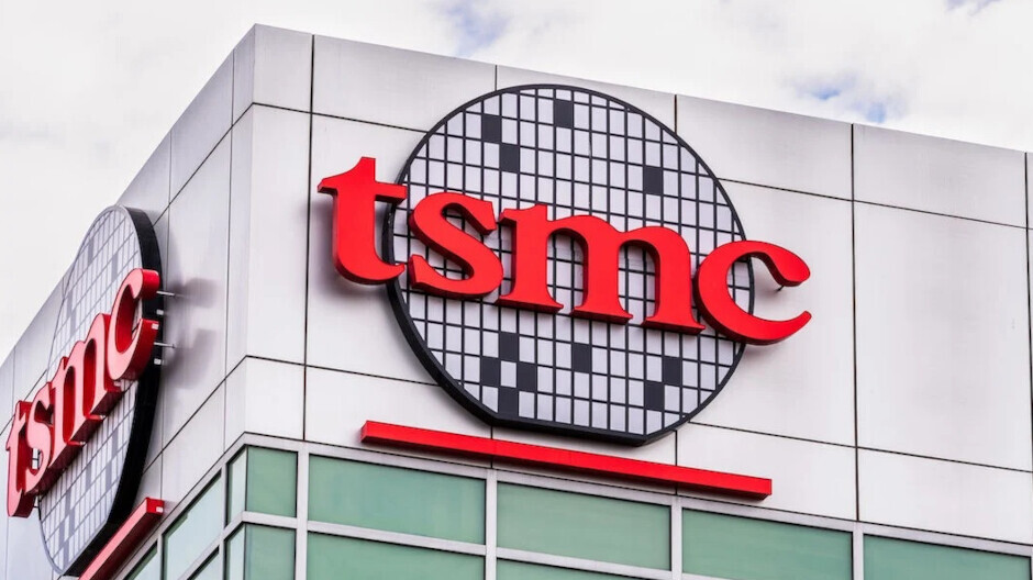
TSMC to Introduce Location Premium for Overseas Chip Production

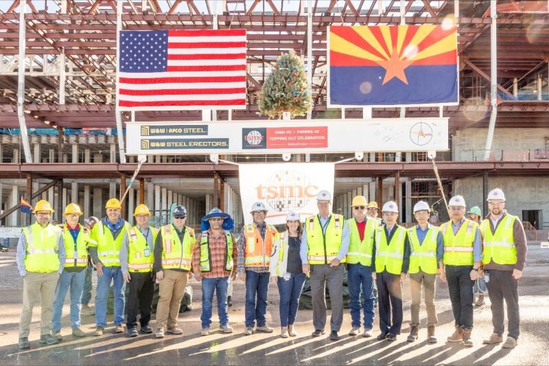
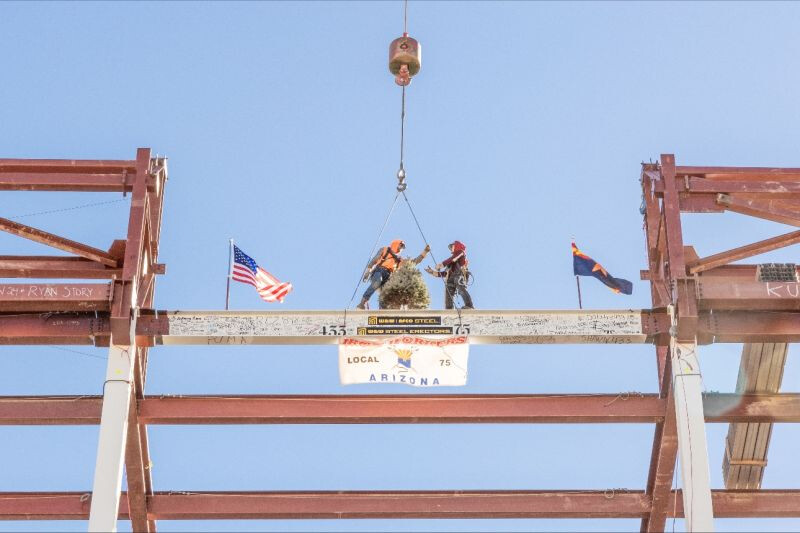
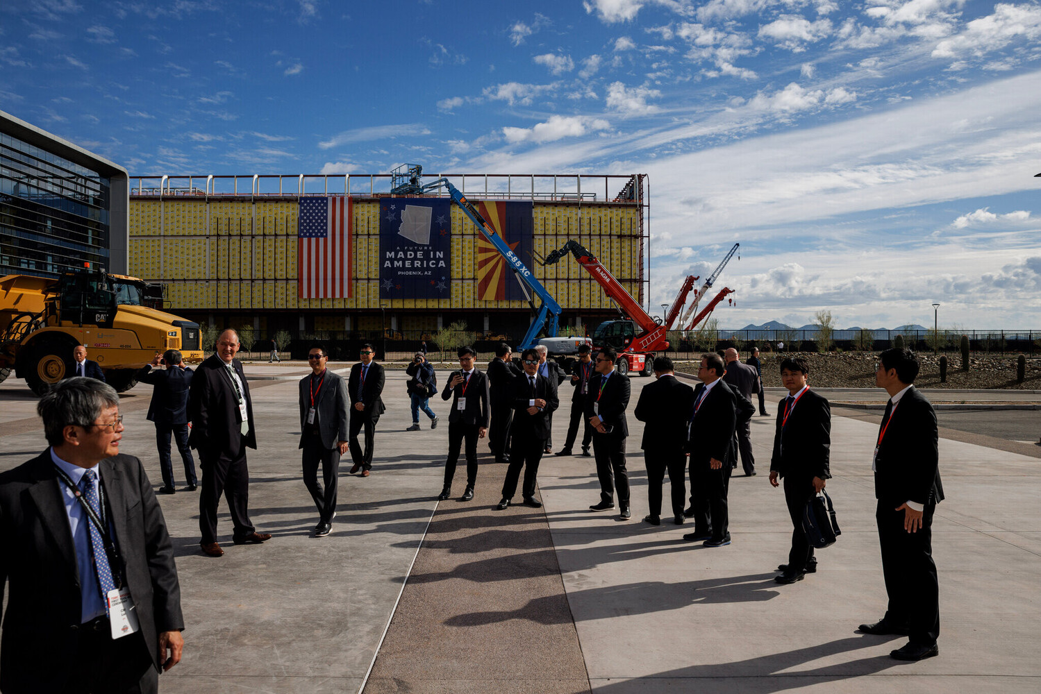
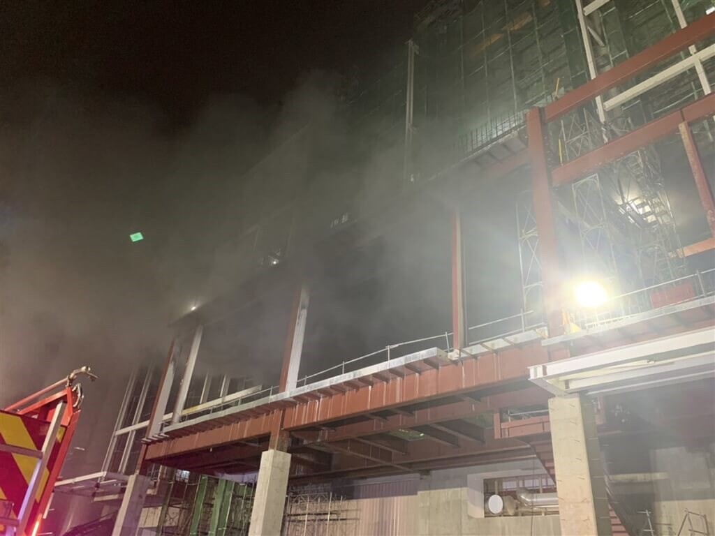
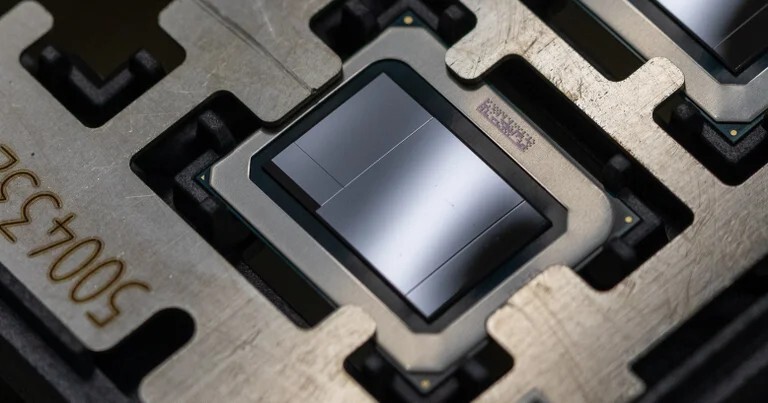
As a part of its Q1 earnings call discussion, one of the largest semiconductor manufacturers, TSMC, has unveiled a strategic move to charge a premium for chips manufactured at its newly established overseas fabrication plants. During an earnings call, TSMC's CEO, C.C. Wei, announced that the company will impose higher pricing for chips produced outside Taiwan to offset the higher operational costs associated with these international locations. This move aims to maintain TSMC's target gross margin of 53% amidst rising expenses such as inflation and elevated electricity costs. This decision comes as TSMC expands its global footprint with new facilities in the United States, Germany, and Japan (JAMS) to meet the increasing demand for semiconductor chips worldwide. The company's new US-based Arizona facility, known as Fab 21, has faced delays due to equipment installation issues and labor negotiations.

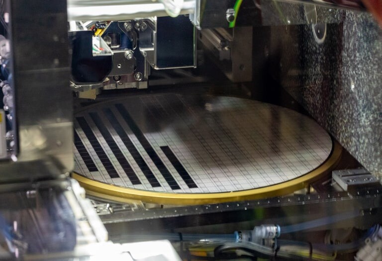
Chips produced at this site, utilizing TSMC's advanced N5 and N4 nodes, could cost between 20% to 30% more than those manufactured in Taiwan. TSMC's strategy to manage the cost disparities across different geographic locations involves strategic pricing, securing government support, and leveraging its manufacturing technology leadership. This approach reflects the company's commitment to maintaining its competitive edge while navigating the complexities of global semiconductor manufacturing in today's fragmented market. Introducing a location premium is expected to impact American semiconductor designers, who may need to pass these costs on to specific market segments, particularly those with lower price sensitivity, such as government-related projects. Despite these challenges, TSMC's overseas expansion underscores its adaptive strategies in the face of global economic pressures and industry demands, ensuring its continued position as a leading player in the semiconductor industry.

Arizona State University and Deca Technologies to Pioneer North America's First R&D Center for Advanced Fan-Out Wafer-Level Packaging

Arizona State University (ASU) and Deca Technologies (Deca), a premier provider of advanced wafer- and panel-level packaging technology, today announced a groundbreaking collaboration to create North America's first fan-out wafer-level packaging (FOWLP) research and development center.

The new Center for Advanced Wafer-Level Packaging Applications and Development is set to catalyze innovation in the United States, expanding domestic semiconductor manufacturing capabilities and driving advancements in cutting-edge fields such as artificial intelligence, machine learning, automotive electronics and high-performance computing.

US Government to Announce Massive Grant for Intel's Arizona Facility

According to the latest report by Reuters, the US government is preparing to announce a multi-billion dollar grant for Intel's chip manufacturing operations in Arizona next week, possibly worth more than $10 billion. US President Joe Biden and Commerce Secretary Gina Raimondo will make the announcement, which is part of the 2022 CHIPS and Science Act aimed at expanding US chip production and reducing dependence on China and Taiwan manufacturing. The exact amount of the grant has yet to be confirmed, but rumors suggest it could exceed $10 billion, making it the most significant award yet under the CHIPS Act. The funding will include grants and loans to bolster Intel's competitive position and support the company's US semiconductor manufacturing expansion plans. This comes as a surprise just a day after the Pentagon reportedly refused to invest $2.5 billion in Intel as a part of a secret defense grant.

Intel has been investing significantly in its US expansion, recently opening a $3.5 billion advanced packaging facility in New Mexico, supposed to create extravagant packaging technology like Foveros and EMIB. The chipmaker is also expanding its semiconductor manufacturing capacity in Arizona, with plans to build new fabs in the state. Arizona is quickly becoming a significant hub for semiconductor manufacturing in the United States. In addition to Intel's expansion, Taiwan Semiconductor Manufacturing Company (TSMC) is also building new fabs in the state, attracting supply partners to the region. CHIPS Act has a total funding capacity of $39 billion allocated for semiconductor production and $11 billion for research and development. The Intel grant will likely cover the production part, as Team Blue has been reshaping its business units with the Intel Product and Intel Foundry segments.

TSMC Arizona Celebrates "Topping Out" Milestone at Second Fab Site

TSMC Arizona's second semiconductor fabrication site has celebrated a "topping out" milestone—as documented in an official blog post (via LinkedIn) from yesterday. Workers were photographed installing an important/final piece of structure—the aforementioned "topping out" milestone signifies: "the last steel beam being raised into place on a construction project." The Taiwanese multinational semiconductor contract manufacturer has had a rough time in establishing operations out in the desert/greater Phoenix area—the "Fab 21 Phase 2" plant is not expected to meet its original 2026 opening window. TSMC Chairman Mark Liu is reportedly leaving his position due to consistent Arizona-related problems and delays.

The TSMC LinkedIn account shared some additional and certainly much-needed positive news: "We also recently achieved the topping milestone on our second fab's auxiliary buildings, which will supply the necessary utilities infrastructure to the second fab clean room." Thursday's blog (February 22) also discloses that the primary site—Fab 21 Phase 1—is still on track to begin production within the first half of 2025, thanks to "significant" bursts in construction progress. The author moved onto future production prospects: "Once operational, our two fabs at TSMC Arizona will manufacture the most advanced semiconductor technology in the U.S., creating 4,500 direct high-tech, high-wage jobs and enabling our customers' leadership in the high-performance computing and artificial intelligence era for decades."

TSMC Delays Launch of Arizona Phase 2 Facility

TSMC's Fab 21 Phase 2 facility is currently under construction in the Greater Phoenix area, Arizona—this secondary production facility was originally announced as housing a 3 nm process production line (opening by 2026), but that company target will be missed by a sizable margin. The transcription of the company's Q4 2023 Earnings Call presents another set of shifted expectations—outgoing CEO, Dr. Mark Liu—admitted that a number of factors are expected to delay Phase 2's opening by another year or two: "The second fab shell is under construction, but what technology [to use] in that shell is still under discussion...I think that also has to do with how much incentives that fab, the U.S. Government can provide…The current planning [for the fab] is '27 or '28, that will be timeframe."

Industry analysts believe TSMC leadership have a tough choice to make—the second Arizona factory's delayed launch could provide enough lead time to upgrade with a more advanced node (e.g. 2 nm), but ambitions could be lowered for the troubled site. An older plus more mature fabrication process could be a better fit, although the neighboring Fab 21 Phase 1 site is already set for a full 2025 initiation on 4 nm FinFET. Liu outlined this challenge: "To be honest, most of the overseas fabs, what technology is being set up, really, it is a decision of customers' demand in that area at that timing. So, nothing is definitive, but we are trying to optimize value for the overseas fab for TSMC." The current chairman will not be around for Phase 1's full deployment, but he shared some positive Arizona-related news: "We are well on track for volume production of N4, or 4 nm process technology, in the first half of 2025 [in Arizona] and are confident that once we begin operations, we will be able to deliver the same level of manufacturing quality and reliability in Arizona as from our fabs in Taiwan."

Apple to Become the First and Largest Customer of Amkor's Arizona Chip Packaging Plant

Apple has announced a partnership deal with Amkor, one of the leading chip packaging and testing manufacturers, which will build a two billion US Dollar silicon packaging facility in Peoria, Arizona. Being the only US-based OSAT (outsourced semiconductor assembly and test) provider, Amkor has decided to invest its funds and apply for the CHIPS Act, hoping to get a part of the funding from the US government's grant budget. The state-of-the-art facility in Arizona will feature over 500,000 square feet (46,452 square meters) of cleanroom space for packaging and testing chips. Using Amkor's latest technologies, the plant will support advanced computing, automotive, and communications chip packaging. It is tailored to meet the capacity needs of major customer Apple starting in 2025-2026. Apple will be the largest customer, with the Amkor facility packaging Apple-designed chips produced at the nearby TSMC wafer fabrication plant.

Building a chip packaging facility in the US with advanced packaging types means that the domestic manufacturing of advanced silicon is now possible across almost the entire supply chain, with OSAT now being present on US soil as well. In the initial phase, this partnership will enable domestic advanced packaging capabilities for leading-edge chips down to 3 nm nodes, which Apple plans to utilize for its A and M series of processors. Along with the creation of an estimated 2,000 local jobs, the investment serves as a boost to the local economy as well. Additionally, Amkor is TSMC's strategic partner, meaning future designs and packaging will cooperate without any delays.

Intel's Arizona Expansion Marks Construction Milestone

Marking a milestone in Intel's ongoing manufacturing expansion in Arizona, the company today announced that the initial portion of the cleanroom is "weather tight" and the "blow down" phase has begun at the company's two new leading-edge chip factories on its Ocotillo campus in Chandler, Arizona. This milestone underscores Intel's dedication to advancing its presence in the state and fostering technological innovation.

"Our commitment to Arizona runs deep, and as we expand our operations, we remain dedicated to addressing the growing demand for semiconductors and helping the United States regain its leadership position in this vital industry. This milestone represents the result of great teamwork, proficient teams and exceptional craftsmanship of the tradespeople, and it's thanks to their hard work that we've made such significant progress on our site while keeping our culture of caring and the safety of all as our top priority." -Dan Doron, Intel vice president and general manager of Fab Construction Enterprise

TSMC Considering Advanced Packaging Request for Arizona Fab

A US delegation has visited Taiwan in order to discuss semiconductor industry partnerships—Katie Hobbs, governor of Arizona, declared that plans for TSMC's Fab 21 facility could be expanded into fairly ambitious areas: "Part of our efforts at building the semiconductor ecosystem is focusing on advanced packaging, so we have several things in the works around that right now." Bloomberg and Reuters report that she attended an important US-Taiwan supply chain forum in Taipei. Mass production at the Phoenix-area foundry has been delayed into 2025, so it is somewhat surprising to hear about greater aspirations for the site. We recently discovered that TSMC will be investing an additional $4.5 billion into its North American subsidiary, but it is too early to say whether this will finance any major upgrades.

TSMC produced a brief statement regarding the latest negotiations: "We believe the dialogues that we held during this visit will help us to work together even more closely in the future." The firm believes that the expansion of advanced chip packaging capacity will alleviate supply constraints—in the context of Taiwanese operations, at least for the moment. The Bloomberg report also focused on another delegate—Laurie E. Locascio, Under Secretary of Commerce—she announced that the North American government is starting to discuss research and development initiatives with TSMC. The key goal being to bring some of that market leading technology and knowledge stateside.

TSMC to Invest Additional $4.5 Billion at Arizona Fab

TSMC has gained the Taiwanese government's approval to invest $4.5 billion in its main North American manufacturing hub—Fab 21 is located in the greater Phoenix area. Mass production at the Arizona foundry has been delayed into 2025 due to behind-schedule equipment installations and various workforce-related issues, but a limited trial run is reported to begin early next year. Mid-last month, the TSMC executive board sought approval from Taiwan's Investment Commission for an additional overseas spend (the Arizona operation is registered as a subsidiary company).

This request was approved by the commission yesterday (September 18)—a $3.5 billion cash injection was already given the thumbs-up back in March. Exact areas of expenditure have not been declared to the public, but Taiwanese media outlets believe that the second phase of funds will be marked for working capital expenses at the North American division. Short-term business costs include the purchase of inventory (e.g raw materials), day-to-day operating expenses and resolvement of short-term debts. Mark Liu, TSMC's chairman, recently expressed optimism about goings-on at Arizona's Fab 21—mentioning significant progress made over the spring and summer period.

Insiders Claim TSMC Arizona Fab to Start Trial Run in Early 2024

Mass production at TSMC's Phoenix, Arizona Fab 21 facility has been delayed until 2025, but the top brass are keen to get some activity started at their North American foundry—it is possible that they want to avoid potential contract breaches, caused by various setbacks. Taiwan's Money DJ (interpreted by TrendForce) reports that a pilot scheme will be implemented by the first quarter of 2024—industry sources believe that a small batch trial run will result in 4000 to 5000 wafer starts per month (WSPM). Setup delays have dropped projected efficiency ratings—analysts reckon that the Arizona plant cannot match the sheer effectiveness of operations back in Taiwan.

TrendForce cites a number of factors, including: "a shortage of skilled equipment installation personnel, local union protests, and differences in overseas safety regulations have caused delays in equipment installation." TSMC chairman Mark Liu expressed optimism about the situation earlier this month—citing significant progress (at the Fab 21 site) over the past five months as an early sign of success for the project. Insiders claim that TSMC is considering a major upgrade of its currently in-construction Japanese facility—extra capacity at the existing location and a second foundry could be on the table.

AMD's Lisa Su Endorses TSMC's Fab 21 Arizona Facility

TSMC is having a tough time getting its Phoenix, Arizona facility up to fully functional standards—large-scale production at Fab 21 has been delayed into 2025 (as announced back in July). Cited factors include workforce-related issues and sluggish installation of state-of-the-art manufacturing equipment. These setbacks are not too disconcerting in the eyes of leadership at AMD—today CEO Dr. Lisa Su declared that her firm will be one of the first in line to contract with TSMC's Fab 21, thanks to long established bonds: "I think we have gotten extremely good at managing supply chain, so I would say that is one of our core strengths. TSMC has been a phenomenal partner for us in terms of advanced technology, both on the silicon side as well as the packaging side, and we very much value that relationship." Su and NVIDIA chief Jensen Huang were key figures present at the Arizona facility's December 2022 opening ceremony.

AMD's top brass is in attendance at this year's Goldman Sachs Communacopia and Technology Conference, alongside arch rival Intel. The latter has already dropped their own revelation for the day. Su commented on North American chip manufacturing circumstances: "When you when you think about the geopolitical situation, geographic diversity is important to us...So, the Arizona factory is very important to us. We are going to be one of the early users, we are putting our first tape outs in shortly with the idea of being a significant user of Arizona. I think we will continue to look at the geographic diversity as an important piece of it." AMD has been fabless since 2009, and relies heavily on TSMC's tried and true Taiwan-based plants to produce CPU, GPU, DPU and FPGA products—it will be interesting to observe how things pan out when some of this output gets shifted over to a fledgling facility positioned out there in the Sonoran desert.

Acer Co-founder Skeptical about US Semiconductor Industry's Prospects

Stan Shih, the co-founder & honorary chairman of Acer Inc., thinks that the USA will have hard time catching up with Asian semiconductor production facilities. Yahoo Taiwan managed to extract some choice comments from the multi-faceted businessman—he believes that the US government's initiative to boost native chip making will not be enough to match existing overseas strongholds. A key area of focus was volume output—Shih reckons that North America is already too far behind Asian counterpart industries, with Acer's home base of Taiwan being particularly strong (in his opinion). Workplace culture and state of the art equipment are cited as the main pillars for success.

Shih observed that that US chip industry has historically been far too reliant on outsourcing (going back many decades) production to foreign facilities, and Asia's position has been fortified thanks to long established and optimized supply chains—he thinks that the American system is not mature enough to reach parity. On a semi-related note, TSMC is reportedly struggling to get its new US facility fully operational—company chairman Mark Liu (according to Tom's Hardware): "said that the Taiwanese company would delay mass production of its Arizona fab from early 2024 to 2025, partly due to a lack of cleanroom tools necessary to produce chips at scale." TSMC has been transferring staff from its home turf to plug staffing gaps at the Phoenix facility—Liu divulged his latest batch of complaints during an earnings conference (last Thursday): "We are encountering certain challenges, as there is an insufficient number of skilled workers with the specialized expertise required for equipment installation in a semiconductor-grade facility."

Intel Atom "Arizona Beach" C1100 Series Sneaks Out

Intel's marketing machine is not always all-encompassing with new product launches—case in point the recent whisper quiet appearance of a trio of "Arizona Beach" Atom SKUs on the market. It took a ServeTheHome reader to inform the publication about edge-based solutions becoming available to clients—mosty notably Silicom's Valencia Network Appliance. Ark site information from 2022 suggested that Team Blue launched its Arizona Beach series last summer, but zero marketing (at their end) has resulted in publications only taking notice a year later. Silicom started advertising its Valencia network models just before Christmas.

The Intel Atom C1100 (dual-core), C1110 (quad-core), and C1130 (octa-core) have been compared to the Alder Lake-N series—at first glance somebody could assume that the new platform is related to older E-core solutions. The site is already familiar with the previous generation since a staffer recently reviewed a Fanless Intel N100 Firewall. The top-end C1130 has a TDP rating of 32 W which comes as mild surprise—this is an Intel 7 part with a 2.5 GHz base and turbo frequency clock, alongside 6 MB L3 cache and 4 MB L2 cache. ServeTheHome compiled their own spec infographic of the Atom SKUs side-by-side, and soon discovered key selling points: support for dual-channel LPDDR5 memory and PCIe Gen 4 in "either 1x x16 + 1x x4 or 2x x8 + 1x x4 configurations." They conclude that the new Atom series has the potential to become an excellent platform for low-power edge devices, the author also hopes that a Mini-ITX option will turn up eventually.

TSMC Boss Responds to Reports of Brutal Corporate Culture

Mark Liu, the executive Chairman of TSMC, has responded to recent reports released by the North American media about supposedly challenging workplace conditions. Current and former employees of the company's U.S operation have taken anonymously to Glassdoor to complain about "brutal" treatment on behalf of TSMC leadership—resulting in a 27% overall approval rating, which sits unfavorably next to the scores of nearby competitors—for example Intel gets 85%, albeit from far more user submissions. Liu has made comments to a Taiwanese news outlet (Focus Taiwan) where he suggests that: "those who are unwilling to take shifts should not enter the industry, since this field isn't just about lucrative wages but rather a passion for (semiconductors)."

TSMC is trying to meet staffing targets for its Phoenix, Arizona operation, but early feedback and difficult residential living could stifle this recruitment drive. Liu thinks that his North American division will offer potential employees a workplace culture that is unlike the one set for crew back in Taiwan. He told the local reporter that American TSMC team members will have an easier time, relative to how things are run at the company's native facilities. He also states that leadership is open to discussions with NA workers, as long as company values are followed (to a tee).

TSMC Employees Experiencing Problems in Arizona

TSMC is having a tough time establishing itself in the United States with new manufacturing facilities - the Taiwanese multinational semiconductor contract manufacturing and design company is putting a great deal of effort into finishing its new Arizona foundry, located in the greater Phoenix area. A minor fire incident occurred at one of their construction sites in late April, and North American news outlets last week reported on the company's struggle to recruit enough staff - approximately 4500 positions - for its upcoming Arizona plants. Current and former employees of TSMC in the U.S. have taken to the Glassdoor review website - user feedback has so far awarded the company a 27% approval rating via 91 submissions, thus warning potential candidates to stay away. Apparently American staffers have found it difficult to adjust to TSMC's corporate culture, and the company could face further challenges when transferring staff from Taiwan.

The latest news from Arizona points to problems encountered at the so-called "TSMC Village" - actually two residential locations divided into "A" and "B" categories. Taiwan's Economic Daily released a video report late last month covering crime-related incidents - this information has since been picked up by Western news outlets. Perpetrators have targeted houses and cars within these new build communities - UDN's footage indicates that seven vehicles located in Village A were damaged with a portion of them broken into. A single Village B property was accessed by possible squatters, and an unspecified number of TSMC engineers have been "robbed" throughout May. Several residents were contacted by UDN - interviewees expressed frustrations with the lack of security in the area, and blamed a local management company for not bolstering prevention measures.

Fire at TSMC Arizona Plant a Minor Episode, North Taiwan Facility Damaged in Separate Incident

TSMC has confirmed to Taiwan News this weekend that a fire at its Phoenix-general area, Arizona semiconductor plant was only "limited to an outside trash chute and immediately extinguished" - the chipmaker was responding to an afternoon incident from Friday (April 28). A worker took photos of black smoke rising from a section of the brand new factory, the employee then proceeded to share their snaps online via a discussion board. A local firefighting crew extinguished the blaze soon after evacuating workers from the affected area, a preliminary investigation conducted by the emergency responders found that the fire originated from a waste/refuse chute. A root cause has not yet been identified according to the newspaper's article.

The Arizona plant was not the only TSMC location to play host to an unexpected incident this week - reports from Wednesday (April 26) state that a fire broke out during the (preceding) evening/night at a company facility in North Taiwan. No injuries or casualties were reported following a response by firefighters who had the situation under control soon after 9 pm - TSMC believes that the fire started at around 19:30. The incomplete factory is situated within Taiwan's Hsinchu Science Park, and is set to bolster the company's existing advanced 3D IC package manufacturing efforts. Part of the facility will also be setup as a component testing lab. TSMC has declared that it is conducting an investigation into the incident at its Zhunan, Miaoli County location.

TSMC Holds 3nm Volume Production and Capacity Expansion Ceremony, Marking a Key Milestone for Advanced Manufacturing

TSMC today held a 3 nanometer (3 nm) Volume Production and Capacity Expansion Ceremony at its Fab 18 new construction site in the Southern Taiwan Science Park (STSP), bringing together suppliers, construction partners, central and local government, the Taiwan Semiconductor Industry Association, and members of academia to witness an important milestone in the Company's advanced manufacturing.

TSMC has laid a strong foundation for 3 nm technology and capacity expansion, with Fab 18 located in the STSP serving as the Company's GIGAFAB facility producing 5 nm and 3 nm process technology. Today, TSMC announced that 3 nm technology has successfully entered volume production with good yields, and held a topping ceremony for its Fab 18 Phase 8 facility. TSMC estimates that 3 nm technology will create end products with a market value of US$1.5 trillion within five years of volume production.

Apple and NVIDIA First Customers of TSMC's Arizona Fab

Apple and NVIDIA will be among the first customers of TSMC's swanky new $12 billion semiconductor fab in Arizona, USA. Apple will be the first major player to kick off mass-production in the fab, and will be closely followed by NVIDIA. Both companies plan to produce some of their inventory in Arizona, and ramp proportionately up as the fab grows in capacity.

The plan with TSMC's Arizona fab was to originally make 5 nm and 4 nm EUV chips, with an output of 20,000 wafers a month, but the company now expects to deploy a more advanced node to keep up with what will be considered cutting-edge when the fab goes live (think 2 nm-class); and also double the output to 40,000 wafers a month. The capacity should ensure Apple and NVIDIA make their most cutting-edge chips on the node (away from Asia), so there could be tighter export controls, and build supply-chain resilience in the face of security problems arising in the Taiwan straits.

TSMC's Morris Chang Says Arizona Fab Will Produce 3 nm Chips in the Future

Although Morris Chang is no longer in charge of the day to day business at TSMC, the founder of the company is still getting his hands dirty. Chang attended the APEC Economic Leaders Meeting last week, as part of Taiwan's delegation and was questioned by the media about TSMC's future plans. The specific question was about TSMC's Arizona fab, which will initially produce chips using a 5 nm node. The US$12 billion plant is scheduled to kick off production at some point in 2024, by which time the 5 nm node should be a commonly used node rather than close to cutting edge.

When questioned about the future of the Arizona fab, Morris Chang answered that it will be moving to a 3 nm node, which is currently TSMC's most cutting edge node, that has gone into volume production earlier this year with th N3 node, which is set to be followed by the N3E node. According to Chang, there's interest by several countries to have TSMC set up fabs there, but apparently this is not something TSMC is considering at the moment. One potential reason for this would be a suitable labour force, something that has already proven to be tough for the Arizona fab.

TSMC Founder Says Growing Domestic US Chip Production is Wasteful and Expensive

According to an article over on The Register, the TSMC founder, Morris Chang, isn't overly impressed by US efforts to grow its domestic chip production. In a podcast hosted by the Brookings Institution, Morris Chang said that the US' attempt to grow its domestic chip production will be "a wasteful, expensive exercise in futility." The reason behind his comment is that he believes the US is lacking the talent to work in the fabs, or possibly the willingness to work triple-shift to keep the fabs running 24/7, unlike the Taiwanese. Furthermore, he states that the US can't compete in terms of cost, as he claims it's 50 percent more expensive to manufacture chips in the US compared to Taiwan.

It should be pointed out that Morris Chang is no longer involved with the day to day operations at TSMC and the above are just his opinion. When questioned about why TSMC is building a fab in Arizona, Chang said that TSMC decided to do it because they were urged to do so by the US government. He also believes that despite government subsidies, the US is unlikely to become self-sufficient when it comes to semiconductors, especially as the cost per chip will be much higher, which will make it hard to compete internationally. However, he does mention that if the PRC decided to start a war with Taiwan, then the bet is likely to pay off for the US, but there are obviously other problems that such a situation would bring as well. Chang also praises US chip design talent and says that Taiwan has very little talent in comparison and that TSMC has none. However, the latter doesn't seem to be entirely true, based on the fact that TSMC is helping its customers to optimise their designs for the various production nodes at TSMC. For those interested, the podcast can be found below.

TSMC Having Problems in Arizona, Increasing Investment in Japan

Things are apparently anything but smooth for TSMC when it comes to its US expansion in Arizona, as reports claim that the construction of its new fab in Arizona is going to be late. This is largely due to labour shortages caused by the pandemic, which in turn is set to delay the entire project. As such, it's being suggested that the installation of manufacturing equipment will be delayed from late Q3 this year until Q1 next year. The knock on effect of this is that production is unlikely to start in Q1 2024 and will most likely be delayed to sometime in the second half of 2024. As a comparison, TSMC normally spends two years to build and configure their fabs in Asia, whereas their first expansion outside of Asia is set to take at least two and a half years.

Another issue is said to be related to finding the right staff, since not only TSMC, but also Intel is looking for competent staff in Arizona. Intel might be the winner here, as TSMC is said to already have complaints from some of its employees, especially from western countries. The main complaint is about excessively long meetings that can add several hours to their workdays. Other complaints revolve around long working hours, as the company employs 12 hour shifts for its engineers and they are often on call over weekends. The company has apparently become increasingly demanding when it comes to its workforce, although TSMC has apparently improved in some ways, based on changes to the Taiwanese labour laws.

Intel "Meteor Lake" Chips Already Being Built at the Arizona Fab

With its 12th Gen Core "Alder Lake-P" mobile processors still on the horizon, Intel is already building test batches of the 14th Gen "Meteor Lake" mobile processors, at its Fab 42 facility in Chandler, Arizona. "Meteor Lake" is a multi-chip module that leverages Intel's Foveros packaging technology to combine "tiles" (purpose built dies) based on different silicon fabrication processes depending on their function and transistor-density/power requirements. It combines four distinct tiles across a single package—the compute tile, with the CPU cores; the graphics tile with the iGPU: the SoC I/O tile, which handles the processor's platform I/O; and a fourth tile, which is currently unknown. This could be a memory stack with similar functions as the HBM stacks on "Sapphire Rapids," or something entirely different.

The compute tile contains the processor's various CPU core types. The P cores are "Redwood Cove," which are two generations ahead of the current "Golden Cove." If Intel's 12-20% generational IPC uplift cadence holds, we're looking at cores with up to 30% higher IPC than "Golden Cove" (50-60% higher than "Skylake."). "Meteor Lake" also debuts Intel's next-generation E-core, codenamed "Crestmont." The compute tile is rumored to be fabricated on the Intel 4 node (optically a 7 nm-class node, but with characteristics similar to TSMC N5).

Intel Wins US Government Project to Develop Leading-Edge Foundry Ecosystem

The U.S. Department of Defense, through the NSTXL consortium-based S2MARTS OTA, has awarded Intel an agreement to provide commercial foundry services in the first phase of its multi-phase Rapid Assured Microelectronics Prototypes - Commercial (RAMP-C) program. The RAMP-C program was created to facilitate the use of a U.S.-based commercial semiconductor foundry ecosystem to fabricate the assured leading-edge custom and integrated circuits and commercial products required for critical Department of Defense systems. Intel Foundry Services, Intel's dedicated foundry business launched this year, will lead the work.

"One of the most profound lessons of the past year is the strategic importance of semiconductors, and the value to the United States of having a strong domestic semiconductor industry. Intel is the sole American company both designing and manufacturing logic semiconductors at the leading edge of technology. When we launched Intel Foundry Services earlier this year, we were excited to have the opportunity to make our capabilities available to a wider range of partners, including in the U.S. government, and it is great to see that potential being fulfilled through programs like RAMP-C." -Pat Gelsinger, Intel CEO.

TSMC Under U.S. Pressure Over China Fab Expansion

TSMC is under pressure from the U.S. to reconsider its plans to expand its facilities in mainland China, sources close to the matter told DigiTimes. TSMC currently operates a fab near Shanghai, and one in Nanjing, which it had originally planned to expand, meeting resistance from the U.S. It is not known if this is government (diplomatic) pressure or by U.S. based customers of TSMC., but is likely a combination of the two. The same forces were possibly behind getting TSMC to invest north of $3.5 billion toward a facility in Arizona with six more "Gigafabs" being planned in the southwestern state. U.S. hand-holding in TSMC's policymaking could be part of a strategy to deny cutting-edge silicon fabrication technology to China (PRC), and to help TSMC expand its manufacturing in safer regions as the security situation across the Taiwan strait continues to deteriorate. TSMC, specifically western tech companies' dependence on it, makes it a soft target on the island, and a bargaining chip to deter western military intervention.

Intel to Enter Third-Party Foundry Business, Set Up $20 Billion Fabs in Arizona

Intel will formally enter the third-party semiconductor foundry business under the Intel Foundry Services (IFS) brand, announced CEO Pat Gelsinger, on Tuesday. This entity would operate under a business model not unlike that of TSMC, with its latest foundry technologies available to third-party customers, besides Intel. The company hopes to become a major foundry service provider to U.S. and E.U. customers, particularly enterprise and government contractors that need secure semiconductor manufacturing on U.S. soil.

To this effect, Gelsinger announced that the company will invest $20 billion in the state of Arizona, to set up two semiconductor foundries. Intel could have an edge over other foundry companies as its foundry service portfolio includes Intel technologies as IP blocks. IFS will be led by semiconductor industry veteran Dr. Randhir Thakur, who will report directly to Pat Gelsinger. The $20 billion investment in Arizona, according to Intel, will generate over 3,000 high-skilled jobs, over 3,000 construction jobs, and approximately 15,000 local long-term jobs.
Return to Keyword Browsing
Apr 30th, 2024 18:13 EDT change timezone

New Forum Posts

Popular Reviews

Controversial News Posts