News Posts matching #Blackwell

Return to Keyword Browsing

AMD's RDNA 4 GPUs Could Stick with 18 Gbps GDDR6 Memory

Today, we have the latest round of leaks that suggest that AMD's upcoming RDNA 4 graphics cards, codenamed the "RX 8000-series," might continue to rely on GDDR6 memory modules. According to Kepler on X, the next-generation GPUs from AMD are expected to feature 18 Gbps GDDR6 memory, marking the fourth consecutive RDNA architecture to employ this memory standard. While GDDR6 may not offer the same bandwidth capabilities as the newer GDDR7 standard, this decision does not necessarily imply that RDNA 4 GPUs will be slow performers. AMD's choice to stick with GDDR6 is likely driven by factors such as meeting specific memory bandwidth requirements and cost optimization for PCB designs. However, if the rumor of 18 Gbps GDDR6 memory proves accurate, it would represent a slight step back from the 18-20 Gbps GDDR6 memory used in AMD's current RDNA 3 offerings, such as the RX 7900 XT and RX 7900 XTX GPUs.

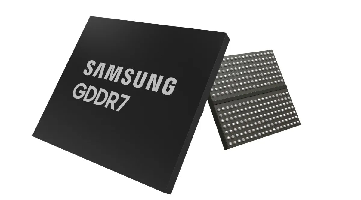
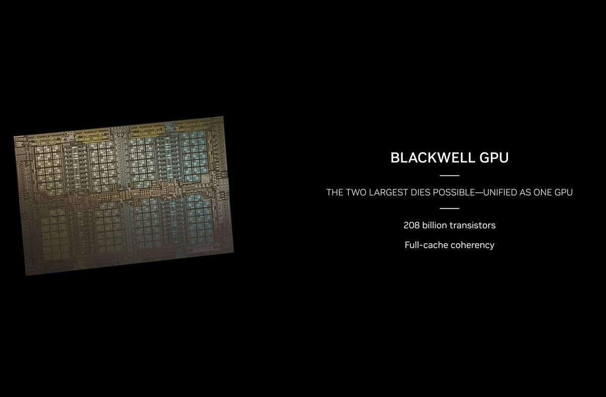
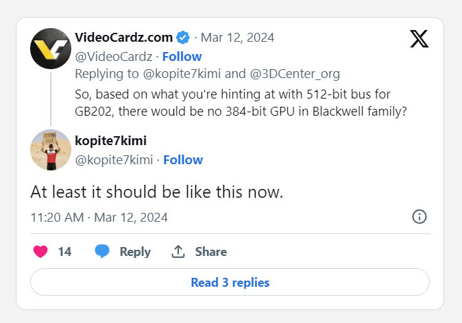
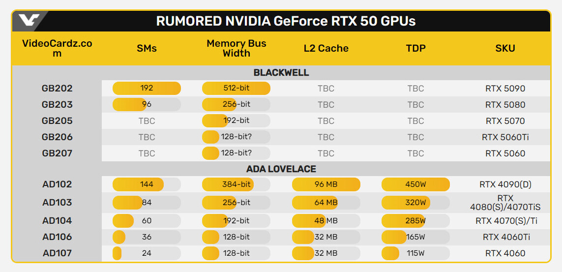
AMD's first generation RDNA used GDDR6 with 12-14 Gbps speeds, RDNA 2 came with GDDR6 at 14-18 Gbps, and the current RDNA 3 used 18-20 Gbps GDDR6. Without an increment in memory generation, speeds should stay the same at 18 Gbps. However, it is crucial to remember that leaks should be treated with skepticism, as AMD's final memory choices for RDNA 4 could change before the official launch. The decision to use GDDR6 versus GDDR7 could have significant implications in the upcoming battle between AMD, NVIDIA, and Intel's next-generation GPU architectures. If AMD indeed opts for GDDR6 while NVIDIA pivots to GDDR7 for its "Blackwell" GPUs, it could create a disparity in memory bandwidth performance between the competing products. All three major GPU manufacturers—AMD, NVIDIA, and Intel with its "Battlemage" architecture—are expected to unveil their next-generation offerings in the fall of this year. As we approach these highly anticipated releases, more concrete details on specifications and performance capabilities will emerge, providing a clearer picture of the competitive landscape.

Demand for NVIDIA's Blackwell Platform Expected to Boost TSMC's CoWoS Total Capacity by Over 150% in 2024

NVIDIA's next-gen Blackwell platform, which includes B-series GPUs and integrates NVIDIA's own Grace Arm CPU in models such as the GB200, represents a significant development. TrendForce points out that the GB200 and its predecessor, the GH200, both feature a combined CPU+GPU solution, primarily equipped with the NVIDIA Grace CPU and H200 GPU. However, the GH200 accounted for only approximately 5% of NVIDIA's high-end GPU shipments. The supply chain has high expectations for the GB200, with projections suggesting that its shipments could exceed millions of units by 2025, potentially making up nearly 40 to 50% of NVIDIA's high-end GPU market.

Although NVIDIA plans to launch products such as the GB200 and B100 in the second half of this year, upstream wafer packaging will need to adopt more complex and high-precision CoWoS-L technology, making the validation and testing process time-consuming. Additionally, more time will be required to optimize the B-series for AI server systems in aspects such as network communication and cooling performance. It is anticipated that the GB200 and B100 products will not see significant production volumes until 4Q24 or 1Q25.

Apple M3 Ultra Chip Could be a Monolithic Design Without UltraFusion Interconnect

As we witness Apple's generational updates of the M series of chips, the highly anticipated SKU of the 3rd generation of Apple M series yet-to-be-announced top-of-the-line M3 Ultra chip is growing speculations from industry insiders. The latest round of reports suggests that the M3 Ultra might step away from its predecessor's design, potentially adopting a monolithic architecture without the UltraFusion interconnect technology. In the past, Apple has relied on a dual-chip design for its Ultra variants, using the UltraFusion interconnect to combine two M series Max chips. For example, the second generation M Ultra chip, M2 Ultra, boasts 134 billion transistors across two 510 mm² chips. However, die-shots of the M3 Max have sparked discussions about the absence of dedicated chip space for the UltraFusion interconnect.

While the absence of visible interconnect space on early die-shots is not conclusive evidence, as seen with the M1 Max not having visible UltraFusion interconnect and still being a part of M1 Ultra with UltraFusion, industry has led the speculation that the M3 Ultra may indeed feature a monolithic design. Considering that the M3 Max has 92 billion transistors and is estimated to have a die size between 600 and 700 mm², going Ultra with these chips may be pushing the manufacturing limit. Considering the maximum die size limit of 848 mm² for the TSMC N3B process used by Apple, there may not be sufficient space for a dual-chip M3 Ultra design. The potential shift to a monolithic design for the M3 Ultra raises questions about how Apple will scale the chip's performance without the UltraFusion interconnect. Competing solutions, such as NVIDIA's Blackwell GPU, use a high-bandwidth C2C interface to connect two 104 billion transistor chips, achieving a bandwidth of 10 TB/s. In comparison, the M2 Ultra's UltraFusion interconnect provided a bandwidth of 2.5 TB/s.

US Government Wants Nuclear Plants to Offload AI Data Center Expansion

The expansion of AI technology affects not only the production and demand for graphics cards but also the electricity grid that powers them. Data centers hosting thousands of GPUs are becoming more common, and the industry has been building new facilities for GPU-enhanced servers to serve the need for more AI. However, these powerful GPUs often consume over 500 Watts per single card, and NVIDIA's latest Blackwell B200 GPU has a TGP of 1000 Watts or a single kilowatt. These kilowatt GPUs will be present in data centers with 10s of thousands of cards, resulting in multi-megawatt facilities. To combat the load on the national electricity grid, US President Joe Biden's administration has been discussing with big tech to re-evaluate their power sources, possibly using smaller nuclear plants. According to an Axios interview with Energy Secretary Jennifer Granholm, she has noted that "AI itself isn't a problem because AI could help to solve the problem." However, the problem is the load-bearing of the national electricity grid, which can't sustain the rapid expansion of the AI data centers.

The Department of Energy (DOE) has been reportedly talking with firms, most notably hyperscalers like Microsoft, Google, and Amazon, to start considering nuclear fusion and fission power plants to satisfy the need for AI expansion. We have already discussed the plan by Microsoft to embed a nuclear reactor near its data center facility and help manage the load of thousands of GPUs running AI training/inference. However, this time, it is not just Microsoft. Other tech giants are reportedly thinking about nuclear as well. They all need to offload their AI expansion from the US national power grid and develop a nuclear solution. Nuclear power is a mere 20% of the US power sourcing, and DOE is currently financing a Holtec Palisades 800-MW electric nuclear generating station with $1.52 billion in funds for restoration and resumption of service. Microsoft is investing in a Small Modular Reactors (SMRs) microreactor energy strategy, which could be an example for other big tech companies to follow.

SK Hynix Plans a $4 Billion Chip Packaging Facility in Indiana

SK Hynix is planning a large $4 billion chip-packaging and testing facility in Indiana, USA. The company is still in the planning stage of the decision to invest in the US. "[the company] is reviewing its advanced chip packaging investment in the US, but hasn't made a final decision yet," a company spokesperson told the Wall Street Journal. The primary product focus for this plant will be stacked HBM memory meant to be consumed by the AI GPU and self-driving automobile industries. The plant could also focus on other exotic memory types, such as high-density server memory; and perhaps even compute-in-memory. The plant is expected to start operations in 2028, and will create up to 1,000 skilled jobs. SK Hynix is counting for state- and federal tax incentives to propel this investment; under government initiatives such as the CHIPS Act. SK Hynix is a significant supplier of HBM to NVIDIA for its AI GPUs. Its HBM3E features in the latest NVIDIA "Blackwell" GPUs.

Product Pages of Samsung 28 Gbps and 32 Gbps GDDR7 Chips Go Live

Samsung is ready with a GDDR7 memory chip rated at an oddly-specific 28 Gbps. This speed aligns with the reported default memory speeds of next-generation NVIDIA GeForce RTX "Blackwell" GPUs. The Samsung GDDR7 memory chip bearing model number K4VAF325ZC-SC28, pictured below, ticks at 3500 MHz, yielding 28 Gbps (GDDR7-effective) memory speeds, and comes with a density of 16 Gbit (2 GB). This isn't Samsung's only GDDR7 chip at launch, the company also has a 32 Gbps high performance part that it built in hopes that certain high-end SKUs or professional graphics cards may implement it. The 32 Gbps GDDR7 chip, bearing the chip model number K4VAF325ZC-SC32, offers the same 16 Gbit density, but at a higher 4000 MHz clock. The Samsung website part-identification pages for both chips say that the parts are sampling to customers, which is usually just before it enters mass-production, and is marked "shipping."

Nvidia CEO Reiterates Solid Partnership with TSMC

One key takeaway from the ongoing GTC is that Nvidia's AI empire has taken shape with strong partnerships from TSMC and other Taiwanese makers, such as those major server ODMs.

According to the news report from the technology-focused media DIGITIMES Asia, during his keynote at GTC on March 18, Huang underscored his company's partnerships with TSMC, as well as the supply chain in Taiwan. Speaking to the press later, Huang said Nvidia will have a very strong demand for CoWoS, the advanced packaging services TSMC offers.

MediaTek Licenses NVIDIA GPU IP for AI-Enhanced Vehicle Processors

NVIDIA has been offering its GPU IP for more than a decade now ever since the introduction of Kepler uArch, and its IP has had relatively low traction in other SoCs. However, that trend seems to be reaching an inflection point as NVIDIA has given MediaTek a license to use its GPU IP to produce the next generation of processors for the auto industry. The newest MediaTek Dimensity Auto Cockpit family consists of CX-1, CY-1, CM-1, and CV-1, where the CX-1 targets premium vehicles, CM targets medium range, and CV targets lower-end vehicles, probably divided by their compute capabilities. The Dimensity Auto Cockpit family is brimming with the latest technology, as the processor core of choice is an Armv9-based design paired with "next-generation" NVIDIA GPU IP, possibly referring to Blackwell, capable of doing ray tracing and DLSS 3, powered by RTX and DLA.

The SoC is supposed to integrate a lot of technology to lower BOM costs of auto manufacturing, and it includes silicon for controlling displays, cameras (advanced HDR ISP), audio streams (multiple audio DSPs), and connectivity (WiFi networking). Interestingly, the SKUs can play movies with AI-enhanced video and support AAA gaming. MediaTek touts the Dimensity Auto Cockpit family with fully local AI processing capabilities, without requiring assistance from outside servers via WiFi, and 3D spatial sensing with driver and occupant monitoring, gaze-aware UI, and natural controls. All of that fits into an SoC fabricated at TSMC's fab on a 3 nm process and runs on the industry-established NVIDIA DRIVE OS.

NVIDIA to Implement GDDR7 Memory on Top-3 "Blackwell" GPUs

NVIDIA is confirmed to implement the GDDR7 memory standard with the top three GPU ASICs powering the next-generation "Blackwell" GeForce RTX 50-series, Tweaktown reports, citing XpeaGPU. By this, we mean the top three physical silicon types from which NVIDIA will carve out the majority of its SKUs. This would include the GB202, the GB203, and GB205; which will power successors to everything from the current RTX 4070 to the RTX 4090. NVIDIA is expected to build these chips on the TSMC 4N foundry node.

There will be certain GPU ASIC types in the "Blackwell" generation that will stick to older memory standards such as GDDR6 or even the GDDR6X. These would be successors to the current AD106 and AD107 ASICs, powering SKUs such as the RTX 4060 Ti, and below. NVIDIA co-developed the GDDR6X standard with Micron Technology, which is the chip's exclusive supplier to NVIDIA. GDDR6X scales up to 23 Gbps and 16 Gbit, which means NVIDIA can avail plenty of performance for the lower-end of its product stack using GDDR6X; especially considering that its GDDR7 implementation will only run at 28 Gbps, despite chips being available in the market for 32 Gbps, or even 36 Gbps. Even if NVIDIA chooses the regular GDDR6 standard for its entry-mainstream chips, the tech scales up to 20 Gbps.

Jensen Huang Discloses NVIDIA Blackwell GPU Pricing: $30,000 to $40,000

Jensen Huang has been talking to media outlets following the conclusion of his keynote presentation at NVIDIA's GTC 2024 conference—an NBC TV "exclusive" interview with the Team Green boss has caused a stir in tech circles. Jim Cramer's long-running "Squawk on the Street" trade segment hosted Huang for just under five minutes—NBC's presenter labelled the latest edition of GTC the "Woodstock of AI." NVIDIA's leader reckoned that around $1 trillion of industry was in attendance at this year's event—folks turned up to witness the unveiling of "Blackwell" B200 and GB200 AI GPUs. In the interview, Huang estimated that his company had invested around $10 billion into the research and development of its latest architecture: "we had to invent some new technology to make it possible."

Industry watchdogs have seized on a major revelation—as disclosed during the televised NBC report—Huang revealed that his next-gen AI GPUs "will cost between $30,000 and $40,000 per unit." NVIDIA (and its rivals) are not known to publicly announce price ranges for AI and HPC chips—leaks from hardware partners and individuals within industry supply chains are the "usual" sources. An investment banking company has already delved into alleged Blackwell production costs—as shared by Tae Kim/firstadopter: "Raymond James estimates it will cost NVIDIA more than $6000 to make a B200 and they will price the GPU at a 50-60% premium to H100...(the bank) estimates it costs NVIDIA $3320 to make the H100, which is then sold to customers for $25,000 to $30,000." Huang's disclosure should be treated as an approximation, since his company (normally) deals with the supply of basic building blocks.

Samsung Shows Off 32 Gbps GDDR7 Memory at GTC

Samsung Electronics showed off its latest graphics memory innovations at GTC, with an exhibit of its new 32 Gbps GDDR7 memory chip. The chip is designed to power the next generation of consumer and professional graphics cards, and some models of NVIDIA's GeForce RTX "Blackwell" generation are expected to implement GDDR7. The chip Samsung showed off at GTC is of the highly relevant 16 Gbit density (2 GB). This is important, as NVIDIA is rumored to keep graphics card memory sizes largely similar to where they currently are, while only focusing on increasing memory speeds.

The Samsung GDDR7 chip shown is capable of its 32 Gbps speed at a DRAM voltage of just 1.1 V, which beats the 1.2 V that's part of JEDEC's GDDR7 specification, which along with other power management innovations specific to Samsung, translates to a 20% improvement in energy efficiency. Although this chip is capable of 32 Gbps, NVIDIA isn't expected to give its first GeForce RTX "Blackwell" graphics cards that speed, and the first SKUs are expected to ship with 28 Gbps GDDR7 memory speeds, which means NVIDIA could run this Samsung chip at a slightly lower voltage, or with better timings. Samsung also made some innovations with the package substrate, which decreases thermal resistance by 70% compared to its GDDR6 chips. Both NVIDIA and AMD are expected to launch their first discrete GPUs implementing GDDR7, in the second half of 2024.

Dell Expands Generative AI Solutions Portfolio, Selects NVIDIA Blackwell GPUs

Dell Technologies is strengthening its collaboration with NVIDIA to help enterprises adopt AI technologies. By expanding the Dell Generative AI Solutions portfolio, including with the new Dell AI Factory with NVIDIA, organizations can accelerate integration of their data, AI tools and on-premises infrastructure to maximize their generative AI (GenAI) investments. "Our enterprise customers are looking for an easy way to implement AI solutions—that is exactly what Dell Technologies and NVIDIA are delivering," said Michael Dell, founder and CEO, Dell Technologies. "Through our combined efforts, organizations can seamlessly integrate data with their own use cases and streamline the development of customized GenAI models."

"AI factories are central to creating intelligence on an industrial scale," said Jensen Huang, founder and CEO, NVIDIA. "Together, NVIDIA and Dell are helping enterprises create AI factories to turn their proprietary data into powerful insights."

NVIDIA "Blackwell" GeForce RTX to Feature Same 5nm-based TSMC 4N Foundry Node as GB100 AI GPU

Following Monday's blockbuster announcements of the "Blackwell" architecture and NVIDIA's B100, B200, and GB200 AI GPUs, all eyes are now on its client graphics derivatives, or the GeForce RTX GPUs that implement "Blackwell" as a graphics architecture. Leading the effort will be the new GB202 ASIC, a successor to the AD102 powering the current RTX 4090. This will be NVIDIA's biggest GPU with raster graphics and ray tracing capabilities. The GB202 is rumored to be followed by the GB203 in the premium segment, the GB205 a notch lower, and the GB206 further down the stack. Kopite7kimi, a reliable source with NVIDIA leaks, says that the GB202 silicon will be built on the same TSMC 4N foundry node as the GB100.

TSMC 4N is a derivative of the company's mainline N4P node, the "N" in 4N stands for NVIDIA. This is a nodelet that TSMC designed with optimization for NVIDIA SoCs. TSMC still considers the 4N as a derivative of the 5 nm EUV node. There is very little public information on the power- and transistor density improvements of the TSMC 4N over TSMC N5. For reference, the N4P, which TSMC regards as a 5 nm derivative, offers a 6% transistor-density improvement, and a 22% power efficiency improvement. In related news, Kopite7kimi says that with "Blackwell," NVIDIA is focusing on enlarging the L1 caches of the streaming multiprocessors (SM), which suggests a design focus on increasing the performance at an SM-level.

Unwrapping the NVIDIA B200 and GB200 AI GPU Announcements

NVIDIA on Monday, at the 2024 GTC conference, unveiled the "Blackwell" B200 and GB200 AI GPUs. These are designed to offer an incredible 5X the AI inferencing performance gain over the current-gen "Hopper" H100, and come with four times the on-package memory. The B200 "Blackwell" is the largest chip physically possible using existing foundry tech, according to its makers. The chip is an astonishing 208 billion transistors, and is made up of two chiplets, which by themselves are the largest possible chips.

Each chiplet is built on the TSMC N4P foundry node, which is the most advanced 4 nm-class node by the Taiwanese foundry. Each chiplet has 104 billion transistors. The two chiplets have a high degree of connectivity with each other, thanks to a 10 TB/s custom interconnect. This is enough bandwidth and latency for the two to maintain cache coherency (i.e. address each other's memory as if they're their own). Each of the two "Blackwell" chiplets has a 4096-bit memory bus, and is wired to 96 GB of HBM3E spread across four 24 GB stacks; which totals to 192 GB for the B200 package. The GPU has a staggering 8 TB/s of memory bandwidth on tap. The B200 package features a 1.8 TB/s NVLink interface for host connectivity, and connectivity to another B200 chip.

ASRock Rack Unveils GPU Servers Supporting NVIDIA Blackwell GB200

ASRock Rack Inc., a leading innovative server company, is announcing its 6U8X-EGS2 series at booth 1617 during the NVIDIA GTC global AI conference in San Jose, USA. The 6U8X-EGS2 NVIDIA H100 and 6U8X-EGS2 NVIDIA H200 are ASRock Rack's most powerful AI training systems, capable of accommodating NVIDIA HGX H200 8-GPUs. The 6U rack mounts are able of providing airflow for the highest CPU and GPU performance. In addition to the eight-way configuration, the 6U8X-EGS2 series offers 12 PCIe Gen 5 NVMe drive bays and multiple PCIe 5.0 x16 slots, as well as a 4+4 PSU for full redundancy.

ASRock Rack is also developing servers that support the new NVIDIA HGX B200 8-GPU to handle the most demanding generative AI applications, accelerate large language models, and cater to data analytics and high-performance computing workloads. "At GTC, NVIDIA announced its new NVIDIA Blackwell platform, and we are glad to contribute to the new era of computing by providing a wide range of server hardware products that will support it," said Hunter Chen, Vice President at ASRock Rack. "Our products provide organizations with the foundation to transform their businesses and leverage the advancements of accelerated computing."

ASUS Presents MGX-Powered Data-Center Solutions

ASUS today announced its participation at the NVIDIA GTC global AI conference, where it will showcase its solutions at booth #730. On show will be the apex of ASUS GPU server innovation, ESC NM1-E1 and ESC NM2-E1, powered by the NVIDIA MGX modular reference architecture, accelerating AI supercomputing to new heights. To help meet the increasing demands for generative AI, ASUS uses the latest technologies from NVIDIA, including the B200 Tensor Core GPU, the GB200 Grace Blackwell Superchip, and H200 NVL, to help deliver optimized AI server solutions to boost AI adoption across a wide range of industries.

To better support enterprises in establishing their own generative AI environments, ASUS offers an extensive lineup of servers, from entry-level to high-end GPU server solutions, plus a comprehensive range of liquid-cooled rack solutions, to meet diverse workloads. Additionally, by leveraging its MLPerf expertise, the ASUS team is pursuing excellence by optimizing hardware and software for large-language-model (LLM) training and inferencing and seamlessly integrating total AI solutions to meet the demanding landscape of AI supercomputing.

Microsoft and NVIDIA Announce Major Integrations to Accelerate Generative AI for Enterprises Everywhere

At GTC on Monday, Microsoft Corp. and NVIDIA expanded their longstanding collaboration with powerful new integrations that leverage the latest NVIDIA generative AI and Omniverse technologies across Microsoft Azure, Azure AI services, Microsoft Fabric and Microsoft 365.

"Together with NVIDIA, we are making the promise of AI real, helping to drive new benefits and productivity gains for people and organizations everywhere," said Satya Nadella, Chairman and CEO, Microsoft. "From bringing the GB200 Grace Blackwell processor to Azure, to new integrations between DGX Cloud and Microsoft Fabric, the announcements we are making today will ensure customers have the most comprehensive platforms and tools across every layer of the Copilot stack, from silicon to software, to build their own breakthrough AI capability."

"AI is transforming our daily lives - opening up a world of new opportunities," said Jensen Huang, founder and CEO of NVIDIA. "Through our collaboration with Microsoft, we're building a future that unlocks the promise of AI for customers, helping them deliver innovative solutions to the world."

AWS and NVIDIA Extend Collaboration to Advance Generative AI Innovation

Amazon Web Services (AWS), an Amazon.com company, and NVIDIA today announced that the new NVIDIA Blackwell GPU platform - unveiled by NVIDIA at GTC 2024 - is coming to AWS. AWS will offer the NVIDIA GB200 Grace Blackwell Superchip and B100 Tensor Core GPUs, extending the companies' long standing strategic collaboration to deliver the most secure and advanced infrastructure, software, and services to help customers unlock new generative artificial intelligence (AI) capabilities.

NVIDIA and AWS continue to bring together the best of their technologies, including NVIDIA's newest multi-node systems featuring the next-generation NVIDIA Blackwell platform and AI software, AWS's Nitro System and AWS Key Management Service (AWS KMS) advanced security, Elastic Fabric Adapter (EFA) petabit scale networking, and Amazon Elastic Compute Cloud (Amazon EC2) UltraCluster hyper-scale clustering. Together, they deliver the infrastructure and tools that enable customers to build and run real-time inference on multi-trillion parameter large language models (LLMs) faster, at massive scale, and at a lower cost than previous-generation NVIDIA GPUs on Amazon EC2.

NVIDIA Launches Blackwell-Powered DGX SuperPOD for Generative AI Supercomputing at Trillion-Parameter Scale

NVIDIA today announced its next-generation AI supercomputer—the NVIDIA DGX SuperPOD powered by NVIDIA GB200 Grace Blackwell Superchips—for processing trillion-parameter models with constant uptime for superscale generative AI training and inference workloads.

Featuring a new, highly efficient, liquid-cooled rack-scale architecture, the new DGX SuperPOD is built with NVIDIA DGX GB200 systems and provides 11.5 exaflops of AI supercomputing at FP4 precision and 240 terabytes of fast memory—scaling to more with additional racks.

NVIDIA Blackwell Platform Arrives to Power a New Era of Computing

Powering a new era of computing, NVIDIA today announced that the NVIDIA Blackwell platform has arrived—enabling organizations everywhere to build and run real-time generative AI on trillion-parameter large language models at up to 25x less cost and energy consumption than its predecessor.

The Blackwell GPU architecture features six transformative technologies for accelerated computing, which will help unlock breakthroughs in data processing, engineering simulation, electronic design automation, computer-aided drug design, quantum computing and generative AI—all emerging industry opportunities for NVIDIA.

Gigabyte Unveils Comprehensive and Powerful AI Platforms at NVIDIA GTC

GIGABYTE Technology and Giga Computing, a subsidiary of GIGABYTE and an industry leader in enterprise solutions, will showcase their solutions at the GIGABYTE booth #1224 at NVIDIA GTC, a global AI developer conference running through March 21. This event will offer GIGABYTE the chance to connect with its valued partners and customers, and together explore what the future in computing holds.

The GIGABYTE booth will focus on GIGABYTE's enterprise products that demonstrate AI training and inference delivered by versatile computing platforms based on NVIDIA solutions, as well as direct liquid cooling (DLC) for improved compute density and energy efficiency. Also not to be missed at the NVIDIA booth is the MGX Pavilion, which features a rack of GIGABYTE servers for the NVIDIA GH200 Grace Hopper Superchip architecture.

NVIDIA B100 "Blackwell" AI GPU Technical Details Leak Out

Jensen Huang's opening GTC 2024 keynote is scheduled to happen tomorrow afternoon (13:00 Pacific time)—many industry experts believe that the NVIDIA boss will take the stage and formally introduce his company's B100 "Blackwell" GPU architecture. An enlightened few have been treated to preview (AI and HPC) units—including Dell's CEO, Jeff Clarke—but pre-introduction leaks have not flowed out. Team Green is likely enforcing strict conditions upon a fortunate selection of trusted evaluators, within a pool of ecosystem partners and customers.

Today, a brave soul has broken that silence—tech tipster, AGF/XpeaGPU, fears repercussions from the leather-jacketed one. They revealed a handful of technical details, a day prior to Team Green's highly anticipated unveiling: "I don't want to spoil NVIDIA B100 launch tomorrow, but this thing is a monster. 2 dies on (TSMC) CoWoS-L, 8x8-Hi HBM3E stacks for 192 GB of memory." They also crystal balled an inevitable follow-up card: "one year later, B200 goes with 12-Hi stacks and will offer a beefy 288 GB. And the performance! It's... oh no Jensen is there... me run away!" Reuters has also joined in on the fun, with some predictions and insider information: "NVIDIA is unlikely to give specific pricing, but the B100 is likely to cost more than its predecessor, which sells for upwards of $20,000." Enterprise products are expected to arrive first—possibly later this year—followed by gaming variants, maybe months later.

NVIDIA Blackwell "GB203" GPU Could Sport 256-bit Memory Interface

Speculative NVIDIA GeForce RTX 50-series "GB20X" GPU memory interface details appeared online late last week—as disclosed by the kopite7kimi social media account. The inside information aficionado—at the time—posited that the "memory interface configuration of GB20x (Blackwell) is not much different from that of AD10x (Ada Lovelace)." It was inferred that Team Green's next flagship gaming GPU (GB202) could debut with a 384-bit memory bus—kopite7kimi had "fantasized" about a potentially monstrous 512-bit spec for the "GeForce RTX 5090." A new batch of follow-up tweets—from earlier today—rips apart last week's insights. The alleged Blackwell GPU gaming lineup includes the following SKUs: GB202, GB203, GB205, GB206, GB207.

Kopite7kimi's revised thoughts point to Team Green's flagship model possessing 192 streaming multiprocessors and a 512-bit memory bus. VideoCardz decided to interact with the reliable tipster—their queries were answered promptly: "According to kopite7kimi, there's a possibility that the second-in-line GPU, named GB203, could sport half of that core count. Now the new information is that GB203 might stick to 256-bit memory bus, which would make it half of GB202 in its entirety. What this also means is that there would be no GB20x GPU with 384-bit bus." Additional speculation has NVIDIA selecting a 192-bit bus for the GB205 SKU (AKA GeForce RTX 5070). The GeForce RTX 50-series is expected to arrive later this year—industry experts are already whispering about HPC-oriented Blackwell GPUs being unveiled at next week's GTC 2024 event. A formal gaming family announcement could arrive many months later.

NVIDIA GeForce RTX 50-series "Blackwell" to use 28 Gbps GDDR7 Memory Speed

The first round of NVIDIA GeForce RTX 50-series "Blackwell" graphics cards that implement GDDR7 memory are rumored to come with a memory speed of 28 Gbps, according to kopite7kimi, a reliable source with NVIDIA leaks. This is despite the fact that the first GDDR7 memory chips will be capable of 32 Gbps speeds. NVIDIA will also stick with 16 Gbit densities for the GDDR7 memory chips, which means memory sizes could remain largely unchanged for the next generation; with the 28 Gbps GDDR7 memory chips providing 55% higher bandwidth over 18 Gbps GDDR6 and 33% higher bandwidth than 21 Gbps GDDR6X. It remains to be seen what memory bus widths NVIDIA chooses for its individual SKUs.

NVIDIA's decision to use 28 Gbps as its memory speeds has some precedent in recent history. The company's first GPUs to implement GDDR6, the RTX 20-series "Turing," opted for 14 Gbps speeds despite 16 Gbps GDDR6 chips being available. 28 Gbps is exactly double that speed. Future generations of GeForce RTX GPUs, or even refreshes within the RTX 50-series could see NVIDIA opt for higher memory speeds such as 32 Gbps. When the standard debuts, companies like Samsung even plan to put up fast 36 Gbps chips. Besides a generational doubling in speeds, GDDR7 is more energy-efficient as it operates at lower voltages than GDDR6. It also uses a more advanced PAM3 physical layer signaling compared to NRZ for JEDEC-standard GDDR6.

Next-Generation NVIDIA DGX Systems Could Launch Soon with Liquid Cooling

During the 2024 SIEPR Economic Summit, NVIDIA CEO Jensen Huang acknowledged that the company's next-generation DGX systems, designed for AI and high-performance computing workloads, will require liquid cooling due to their immense power consumption. Huang also hinted that these new systems are set to be released in the near future. The revelation comes as no surprise, given the increasing power of GPUs needed to satisfy AI and machine learning applications. As computational requirements continue to grow, so does the need for more powerful hardware. However, with great power comes great heat generation, necessitating advanced cooling solutions to maintain optimal performance and system stability. Liquid cooling has long been a staple in high-end computing systems, offering superior thermal management compared to traditional air cooling methods.

By implementing liquid cooling in the upcoming DGX systems, NVIDIA aims to push the boundaries of performance while ensuring the hardware remains reliable and efficient. Although Huang did not provide a specific release date for the new DGX systems, his statement suggests that they are on the horizon. Whether the next generation of DGX systems uses the current NVIDIA H200 or the upcoming Blackwell B100 GPU as their primary accelerator, the performance will undoubtedly be delivered. As the AI and high-performance computing landscape continues to evolve, NVIDIA's position continues to strengthen, and liquid-cooled systems will certainly play a crucial role in shaping the future of these industries.
Return to Keyword Browsing
May 1st, 2024 04:44 EDT change timezone

New Forum Posts

Popular Reviews

Controversial News Posts