News Posts matching #DRAM

Return to Keyword Browsing

Enthusiast Transforms QLC SSD Into SLC With Drastic Endurance and Performance Increase

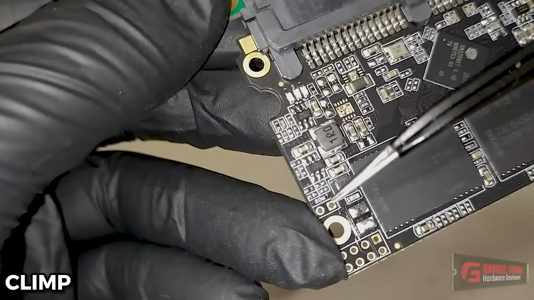
A few months ago, we covered proof of overclocking an off-the-shelf 2.5-inch SATA III NAND Flash SSD thanks to Gabriel Ferraz, Computer Engineer and TechPowerUp's SSD database maintainer. Now, he is back with another equally interesting project of modifying a Quad-Level Cell (QLC) SATA III SSD into a Single-Level Cell (SLC) SATA III SSD. Using the Crucial BX500 512 GB SSD, he aimed at transforming the QLC drive into a more endurant and higher-performance SLC. Silicon Motion SM2259XT2 powers the drive of choice with a single-core ARC 32-bit CPU clocked at 550 MHz and two channels running at 800 MT/s (400 MHz) without a DRAM cache. This particular SSD uses four NAND Flash dies from Micron with NY240 part numbers. Two dies are controlled per channel. These NAND Flash dies were designed to operate at 1,600 MT/s (800 MHz) but are limited to only 525 MT/s in this drive in the real world.

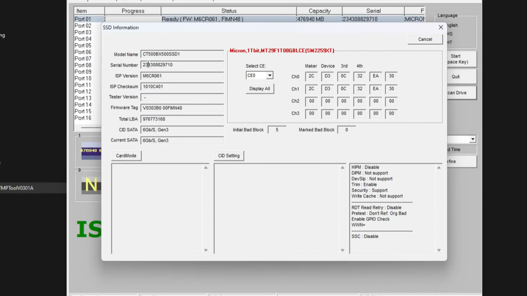
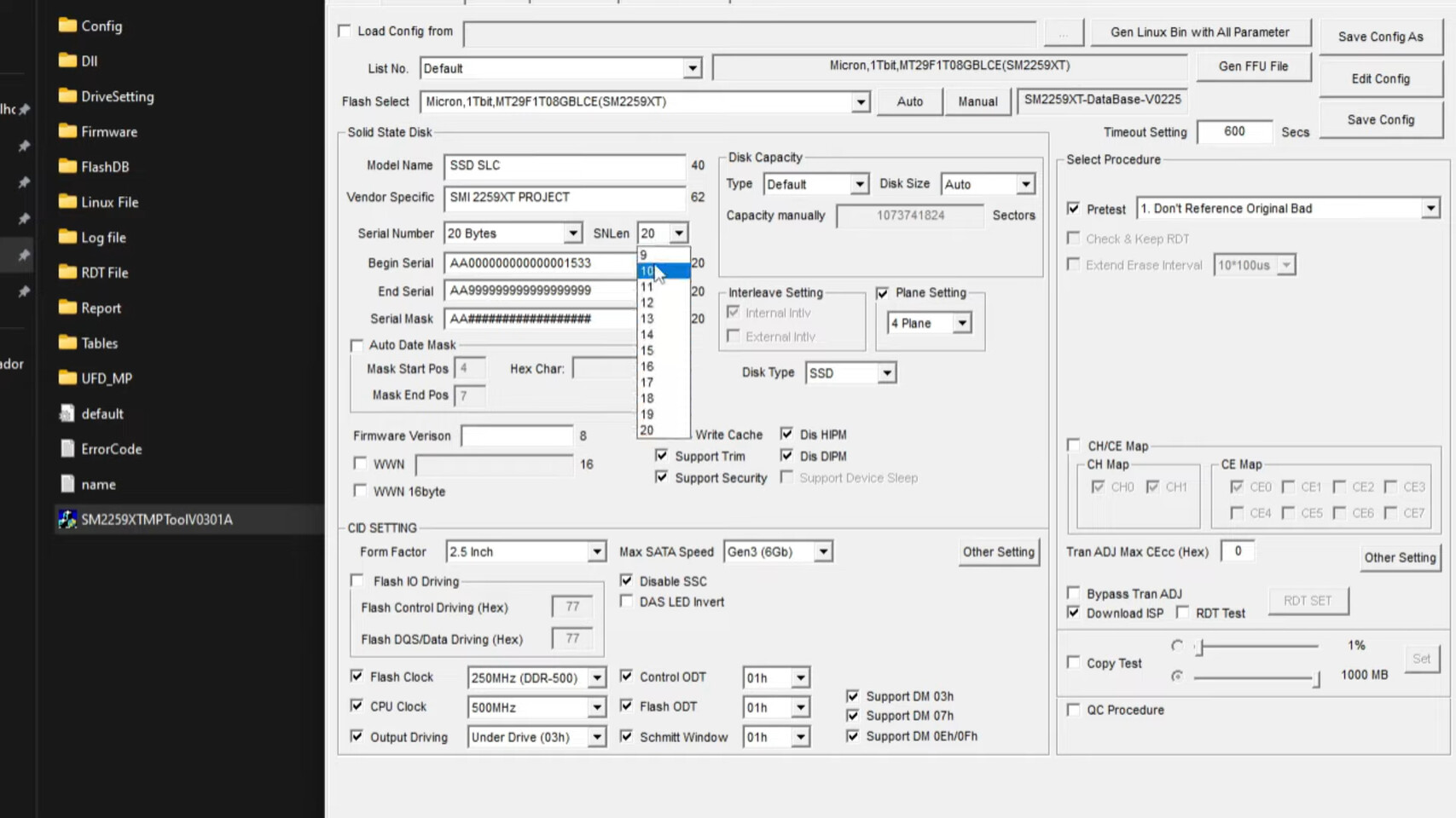
The average endurance of these dies is 1,500 P/E cycles in NANDs FortisFlash and about 900 P/E cycles in Mediagrade. Transforming the same drive in the pSLC is bumping those numbers to 100,000 and 60,000, respectively. However, getting that to work is the tricky part. To achieve this, you have to download MPtools for the Silicon Motion SM2259XT2 controller from the USBdev.ru website and find the correct die used in the SSD. Then, the software is modified carefully, and a case-sensitive configuration file is modified to allow for SLC mode, which forces the die to run as a SLC NAND Flash die. Finally, firmware folder must be reached and files need to be moved arround in a way seen in the video.

SK hynix Strengthens AI Memory Leadership & Partnership With Host at the TSMC 2024 Tech Symposium

SK hynix showcased its next-generation technologies and strengthened key partnerships at the TSMC 2024 Technology Symposium held in Santa Clara, California on April 24. At the event, the company displayed its industry-leading HBM AI memory solutions and highlighted its collaboration with TSMC involving the host's CoWoS advanced packaging technology.

TSMC, a global semiconductor foundry, invites its major partners to this annual conference in the first half of each year so they can share their new products and technologies. Attending the event under the slogan "Memory, the Power of AI," SK hynix received significant attention for presenting the industry's most powerful AI memory solution, HBM3E. The product has recently demonstrated industry-leading performance, achieving input/output (I/O) transfer speed of up to 10 gigabits per second (Gbps) in an AI system during a performance validation evaluation.

Micron to Receive US$6.1 Billion in CHIPS and Science Act Funding

Micron Technology, Inc., one of the world's largest semiconductor companies and the only U.S.-based manufacturer of memory, and the Biden-Harris Administration today announced that they have signed a non-binding Preliminary Memorandum of Terms (PMT) for $6.1 billion in funding under the CHIPS and Science Act to support planned leading-edge memory manufacturing in Idaho and New York.

The CHIPS and Science Act grants of $6.1 billion will support Micron's plans to invest approximately $50 billion in gross capex for U.S. domestic leading-edge memory manufacturing through 2030. These grants and additional state and local incentives will support the construction of one leading-edge memory manufacturing fab to be co-located with the company's existing leading-edge R&D facility in Boise, Idaho and the construction of two leading-edge memory fabs in Clay, New York.

SK Hynix Announces 1Q24 Financial Results

SK hynix Inc. announced today that it recorded 12.43 trillion won in revenues, 2.886 trillion won in operating profit (with an operating margin of 23%), and 1.917 trillion won in net profit (with a net margin of 15%) in the first quarter. With revenues marking an all-time high for a first quarter and the operating profit a second-highest following the records of the first quarter of 2018, SK hynix believes that it has entered the phase of a clear rebound following a prolonged downturn.

The company said that an increase in the sales of AI server products backed by its leadership in AI memory technology including HBM and continued efforts to prioritize profitability led to a 734% on-quarter jump in the operating profit. With the sales ratio of eSSD, a premium product, on the rise and the average selling prices rising, the NAND business has also achieved a meaningful turnaround in the same period.

SMART Modular Technologies Introduces New Family of CXL Add-in Cards for Memory Expansion

SMART Modular Technologies, Inc. ("SMART"), a division of SGH (Nasdaq: SGH) and a global leader in memory solutions, solid-state drives, and advanced memory, announces its new family of Add-In Cards (AICs) which implements the Compute Express Link (CXL) standard and also supports industry standard DDR5 DIMMs. These are the first in their class, high-density DIMM AICs to adopt the CXL protocol. The SMART 4-DIMM and 8-DIMM products enable server and data center architects to add up to 4 TB of memory in a familiar, easy-to-deploy form factor.

"The market for CXL memory components for data center applications is expected to grow rapidly. Initial production shipments are expected in late 2024 and will surpass the $2 billion mark by 2026. Ultimately, CXL attach rates in the server market will reach 30% including both expansion and pooling use cases," stated Mike Howard, vice president of DRAM and memory markets at TechInsights, an intelligence source to semiconductor innovation and related markets.

SK hynix to Produce DRAM from M15X in Cheongju

SK hynix Inc. announced today that it plans to expand production capacity of the next-generation DRAM including HBM, a core component of the AI infrastructure, in response to the rapidly increasing demand for AI semiconductors. As the board of directors approves the plan, the company will build the M15X fab in Cheongju, North Chungcheong Province, for a new DRAM production base, and invest about 5.3 trillion won for fab construction.

The company plans to start construction at the end of April with an aim to complete in November 2025 for an early mass production. With a gradual increase in equipment investment planned, the total investment in building the new production base will be more than 20 trillion won in the long-term. As a global leader in AI memory, SK hynix expects the expansion in investment to contribute to revitalizing the domestic economy, while refreshing Korea's reputation as a semiconductor powerhouse.

JEDEC Updates DDR5 Specification for Increased Security Against Rowhammer Attacks, New DDR5-8800 Reference Speed

JEDEC Solid State Technology Association, the global leader in standards development for the microelectronics industry, today announced publication of the JESD79-5C DDR5 SDRAM standard. This important update to the JEDEC DDR5 SDRAM standard includes features designed to improve reliability and security and enhance performance in a wide range of applications from high-performance servers to emerging technologies such as AI and machine learning. JESD79-5C is now available for download from the JEDEC website.

JESD79-5C introduces an innovative solution to improve DRAM data integrity called Per-Row Activation Counting (PRAC). PRAC precisely counts DRAM activations on a wordline granularity. When PRAC-enabled DRAM detects an excessive number of activations, it alerts the system to pause traffic and to designate time for mitigative measures. These interrelated actions underpin PRAC's ability to provide a fundamentally accurate and predictable approach for addressing data integrity challenges through close coordination between the DRAM and the system.

SK hynix Collaborates with TSMC on HBM4 Chip Packaging

SK hynix Inc. announced today that it has recently signed a memorandum of understanding with TSMC for collaboration to produce next-generation HBM and enhance logic and HBM integration through advanced packaging technology. The company plans to proceed with the development of HBM4, or the sixth generation of the HBM family, slated to be mass-produced from 2026, through this initiative.

SK hynix said the collaboration between the global leader in the AI memory space and TSMC, a top global logic foundry, will lead to more innovations in HBM technology. The collaboration is also expected to enable breakthroughs in memory performance through trilateral collaboration between product design, foundry, and memory provider. The two companies will first focus on improving the performance of the base die that is mounted at the very bottom of the HBM package. HBM is made by stacking a core DRAM die on top of a base die that features TSV technology, and vertically connecting a fixed number of layers in the DRAM stack to the core die with TSV into an HBM package. The base die located at the bottom is connected to the GPU, which controls the HBM.

Samsung Develops Industry's Fastest 10.7Gbps LPDDR5X DRAM

Samsung Electronics, a world leader in advanced memory technology, today announced that it has developed the industry's first LPDDR5X DRAM supporting the industry's highest performance of up to 10.7 gigabits-per-second (Gbps). Leveraging 12 nanometer (nm)-class process technology, Samsung has achieved the smallest chip size among existing LPDDRs, solidifying its technological leadership in the low-power DRAM market.

"As demand for low-power, high-performance memory increases, LPDDR DRAM is expected to expand its applications from mainly mobile to other areas that traditionally require higher performance and reliability such as PCs, accelerators, servers and automobiles," said YongCheol Bae, Executive Vice President of Memory Product Planning of the Memory Business at Samsung Electronics. "Samsung will continue to innovate and deliver optimized products for the upcoming on-device AI era through close collaboration with customers." With the surge in AI applications, on-device AI, which enables direct processing on devices, is becoming increasingly crucial, underscoring the need for low-power, high-performance LPDDR memory.

Montage Technology Pioneers the Trial Production of DDR5 CKDs

Montage Technology, a leading data processing and interconnect IC company, today announced that it has taken the lead in the trial production of 1st-generation DDR5 Clock Driver (CKD) chips for next-generation client memory. This new product aims to enhance the speed and stability of memory data access to match the ever-increasing CPU operating speed and performance.

Previously, clock driver functionality was integrated into the Registering Clock Driver (RCD) chips used on server RDIMM or LRDIMM modules, not deployed to the PCs. In the DDR5 era, as data rates climb 6400 MT/s and above, the clock driver has emerged as an indispensable component for client memory.

DRAM Manufacturers Gradually Resume Production, Impact on Total Q2 DRAM Output Estimated to Be Less Than 1%

Following in the wake of an earthquake that struck on April 3rd, TrendForce undertook an in-depth analysis of its effects on the DRAM industry, uncovering a sector that has shown remarkable resilience and faced minimal interruptions. Despite some damage and the necessity for inspections or disposal of wafers among suppliers, the facilities' strong earthquake preparedness of the facilities has kept the overall impact to a minimum.

Leading DRAM producers, including Micron, Nanya, PSMC, and Winbond had all returned to full operational status by April 8th. In particular, Micron's progression to cutting-edge processes—specifically the 1alpha and 1beta nm technologies—is anticipated to significantly alter the landscape of DRAM bit production. In contrast, other Taiwanese DRAM manufacturers are still working with 38 and 25 nm processes, contributing less to total output. TrendForce estimates that the earthquake's effect on DRAM production for the second quarter will be limited to a manageable 1%.

Micron Debuts World's First Quad-Port SSD to Accelerate Data-Rich Autonomous and AI-Enabled Workloads

Micron Technology, Inc., today announced it is sampling the automotive-grade Micron 4150AT SSD, the world's first quad-port SSD, capable of interfacing with up to four systems on chips (SoCs) to centralize storage for software-defined intelligent vehicles. The Micron 4150AT SSD combines market-leading features such as single-root input/output virtualization (SR-IOV), a PCIe Generation 4 interface and ruggedized automotive design. With these features, the automotive-grade SSD provides the ecosystem with data center-level flexibility and power.

"As storage requirements race to keep up with rich in-vehicle experiences featuring AI and advanced algorithms for higher levels of autonomous safety, this era demands a new paradigm for automotive storage to match," said Michael Basca, Micron vice president of embedded products and systems. "Building on our collaboration with the innovators redefining next-generation automotive architectures, Micron has reimagined storage from the ground up to deliver the world's first quad-port SSD - the Micron 4150AT - which provides the industry flexibility and horsepower to roll out the transformative technologies on the horizon."

SK hynix Signs Investment Agreement of Advanced Chip Packaging with Indiana

SK hynix Inc., the world's leading producer of High-Bandwidth Memory (HBM) chips, announced today that it will invest an estimated $3.87 billion in West Lafayette, Indiana to build an advanced packaging fabrication and R&D facility for AI products. The project, the first of its kind in the United States, is expected to drive innovation in the nation's AI supply chain, while bringing more than a thousand new jobs to the region.

The company held an investment agreement ceremony with officials from Indiana State, Purdue University, and the U.S. government at Purdue University in West Lafayette on the 3rd and officially announced the plan. At the event, officials from each party including Governor of Indiana Eric Holcomb, Senator Todd Young, Director of the White House Office of Science and Technology Policy Arati Prabhakar, Assistant Secretary of Commerce Arun Venkataraman, Secretary of Commerce State of Indiana David Rosenberg, Purdue University President Mung Chiang, Chairman of Purdue Research Foundation Mitch Daniels, Mayor of city of West Lafayette Erin Easter, Ambassador of the Republic of Korea to the United States Hyundong Cho, Consul General of the Republic of Korea in Chicago Junghan Kim, SK vice chairman Jeong Joon Yu, SK hynix CEO Kwak Noh-Jung and SK hynix Head of Package & Test Choi Woojin, participated.

Phison Collaborates with MediaTek to Propel Generative AI Computing and Services

Phison Electronics, a leading provider of NAND controllers and NAND storage solutions, today announced a pivotal strategic collaboration with industry giant MediaTek to push forward innovations in generative artificial intelligence (Generative AI) computing and services, and meet demand for fine-tuning AI model computations across industries. Under the collaboration, Phison's cutting-edge AI computing service, aiDAPTIV+, will pair with MediaTek's premier generative AI service platform, MediaTek DaVinci, heralding a new epoch for AI computing and application services and accelerating the adoption of generative AI in everyday life.

MediaTek DaVinci is an advanced, open platform for generative AI services, built on the Generative AI Service Framework (GAISF). MediaTek DaVinci enables developers to build a variety of plugins for enterprise applications, fostering a vibrant ecosystem and enhancing the user experience. Phison's aiDAPTIV+ features a pioneering SSD-integrated AI computing architecture that breaks down large AI models for concurrent operation with SSDs. This approach significantly reduces infrastructure costs and boosts computational efficiency, enabling the training of substantial AI models with limited GPU and DRAM resources. aiDAPTIV+ has already demonstrated its effectiveness in the Industry 4.0 sector and is poised to accelerate AI transformation across various sectors, bolstering business competitiveness. Additionally, aiDAPTIV+ consumes less power than traditional AI server setups for the same AI model fine-tuning tasks and this aligns with the current trend of minimizing energy consumption and carbon footprint.

Suppliers Aim to Raise Contract Prices, But With Uncertain Demand, 2Q24 DRAM Price Increase Expected to Narrow to 3-8%

TrendForce's latest report reveals that despite DRAM suppliers' efforts to trim inventories, they have yet to reach healthy ranges. As they continue to improve their lose situations by boosting capacity utilization rates, the overall demand outlook for this year remains tepid. Additionally, significant price increases by suppliers since 4Q23 are expected to further diminish the momentum for inventory restocking. As a result, DRAM contract prices for the second quarter are projected to see a modest increase of 3-8%.

The shift toward DDR5-compatible CPUs is set to drive an increase in PC DRAM demand in the second quarter. As manufacturers move toward more advanced, cost-efficient production processes for DDR5, their profitability is expected to rise significantly. This anticipation of higher DRAM prices in 1H24 has led to suppliers to aim for price increases in Q2, targeting a 3-8% hike in PC DRAM contract prices. Notably, even though DDR5 prices have already seen a notable rise in Q1—exceeding the average increase for other products—the expected emergence of AI PC demand may lead to a slight moderation in DDR5 price increases in Q2.

SK hynix Unveils Highest-Performing SSD for AI PCs at NVIDIA GTC 2024

SK hynix unveiled a new consumer product based on its latest solid-state drive (SSD), PCB01, which boasts industry-leading performance levels at GPU Technology Conference (GTC) 2024. Hosted by NVIDIA in San Jose, California from March 18-21, GTC is one of the world's leading conferences for AI developers. Applied to on-device AI PCs, PCB01 is a PCIe fifth-generation SSD which recently had its performance and reliability verified by a major global customer. After completing product development in the first half of 2024, SK hynix plans to launch two versions of PCB01 by the end of the year which target both major technology companies and general consumers.

Optimized for AI PCs, Capable of Loading LLMs Within One Second
Offering the industry's highest sequential read speed of 14 gigabytes per second (GB/s) and a sequential write speed of 12 GB/s, PCB01 doubles the speed specifications of its previous generation. This enables the loading of LLMs required for AI learning and inference in less than one second. To make on-device AIs operational, PC manufacturers create a structure that stores an LLM in the PC's internal storage and quickly transfers the data to DRAMs for AI tasks. In this process, the PCB01 inside the PC efficiently supports the loading of LLMs. SK hynix expects these characteristics of its latest SSD to greatly increase the speed and quality of on-device AIs.

Samsung Shows Off 32 Gbps GDDR7 Memory at GTC

Samsung Electronics showed off its latest graphics memory innovations at GTC, with an exhibit of its new 32 Gbps GDDR7 memory chip. The chip is designed to power the next generation of consumer and professional graphics cards, and some models of NVIDIA's GeForce RTX "Blackwell" generation are expected to implement GDDR7. The chip Samsung showed off at GTC is of the highly relevant 16 Gbit density (2 GB). This is important, as NVIDIA is rumored to keep graphics card memory sizes largely similar to where they currently are, while only focusing on increasing memory speeds.

The Samsung GDDR7 chip shown is capable of its 32 Gbps speed at a DRAM voltage of just 1.1 V, which beats the 1.2 V that's part of JEDEC's GDDR7 specification, which along with other power management innovations specific to Samsung, translates to a 20% improvement in energy efficiency. Although this chip is capable of 32 Gbps, NVIDIA isn't expected to give its first GeForce RTX "Blackwell" graphics cards that speed, and the first SKUs are expected to ship with 28 Gbps GDDR7 memory speeds, which means NVIDIA could run this Samsung chip at a slightly lower voltage, or with better timings. Samsung also made some innovations with the package substrate, which decreases thermal resistance by 70% compared to its GDDR6 chips. Both NVIDIA and AMD are expected to launch their first discrete GPUs implementing GDDR7, in the second half of 2024.

SK Hynix Begins Volume Production of Industry's First HBM3E

SK hynix Inc. announced today that it has begun volume production of HBM3E, the newest AI memory product with ultra-high performance, for supply to a customer from late March. The company made public its success with the HBM3E development just seven months ago. SK hynix being the first provider of HBM3E, a product with the best performing DRAM chips, extends its earlier success with HBM3. The company expects a successful volume production of HBM3E, along with its experiences also as the industry's first provider of HBM3, to help cement its leadership in the AI memory space.

In order to build a successful AI system that processes a huge amount of data quickly, a semiconductor package should be composed in a way that numerous AI processors and memories are multi-connected. Global big tech companies have been increasingly requiring stronger performance of AI semiconductor and SK hynix expects its HBM3E to be their optimal choice that meets such growing expectations.

2024 HBM Supply Bit Growth Estimated to Reach 260%, Making Up 14% of DRAM Industry

TrendForce reports that significant capital investments have occurred in the memory sector due to the high ASP and profitability of HBM. Senior Vice President Avril Wu notes that by the end of 2024, the DRAM industry is expected to allocate approximately 250K/m (14%) of total capacity to producing HBM TSV, with an estimated annual supply bit growth of around 260%. Additionally, HBM's revenue share within the DRAM industry—around 8.4% in 2023—is projected to increase to 20.1% by the end of 2024.

HBM supply tightens with order volumes rising continuously into 2024
Wu explains that in terms of production differences between HBM and DDR5, the die size of HBM is generally 35-45% larger than DDR5 of the same process and capacity (for example, 24Gb compared to 24Gb). The yield rate (including TSV packaging) for HBM is approximately 20-30% lower than that of DDR5, and the production cycle (including TSV) is 1.5 to 2 months longer than DDR5.

JEDEC Agrees to Relax HBM4 Package Thickness

JEDEC is currently presiding over standards for 6th generation high bandwidth memory (AKA HBM4)—the 12 and 16-layer DRAM designs are expected to reach mass production status in 2026. According to a ZDNET South Korea report, involved manufacturers are deliberating over HBM4 package thicknesses—allegedly, decision makers have settled on 775 micrometers (μm). This is thicker than the previous generation's measurement of 720 micrometers (μm). Samsung Electronics, SK Hynix and Micron are exploring "hybrid bonding," a new packaging technology—where onboard chips and wafers are linked directly to each other. Hybrid bonding is expected to be quite expensive to implement, so memory makers are carefully considering whether HBM4 warrants its usage.

ZDNET believes that JEDEC's agreement—settling on 775 micrometers (μm) for 12-layer and 16-layer stacked HBM4—could have: "a significant impact on the future packaging investment trends of major memory manufacturers. These companies have been preparing a new packaging technology, hybrid bonding, keeping in mind the possibility that the package thickness of HBM4 will be limited to 720 micrometers. However, if the package thickness is adjusted to 775 micrometers, 16-layer DRAM stacking HBM4 can be sufficiently implemented using existing bonding technology." A revised schedule could delay the rollout of hybrid bonding—perhaps pushed back to coincide with a launch of seventh generation HBM. The report posits that Samsung Electronics, SK Hynix and Micron memory engineers are about to focus on the upgrading of existing bonding technologies.

Global Top 10 Foundries Q4 Revenue Up 7.9%, Annual Total Hits US$111.54 Billion in 2023

The latest TrendForce report reveals a notable 7.9% jump in 4Q23 revenue for the world's top ten semiconductor foundries, reaching $30.49 billion. This growth is primarily driven by sustained demand for smartphone components, such as mid and low-end smartphone APs and peripheral PMICs. The launch season for Apple's latest devices also significantly contributed, fueling shipments for the A17 chipset and associated peripheral ICs, including OLED DDIs, CIS, and PMICs. TSMC's premium 3 nm process notably enhanced its revenue contribution, pushing its global market share past the 60% threshold this quarter.

TrendForce remarks that 2023 was a challenging year for foundries, marked by high inventory levels across the supply chain, a weak global economy, and a slow recovery in the Chinese market. These factors led to a downward cycle in the industry, with the top ten foundries experiencing a 13.6% annual drop as revenue reached just $111.54 billion. Nevertheless, 2024 promises a brighter outlook, with AI-driven demand expected to boost annual revenue by 12% to $125.24 billion. TSMC, benefiting from steady advanced process orders, is poised to far exceed the industry average in growth.

JEDEC Publishes GDDR7 Graphics Memory Standard

JEDEC Solid State Technology Association, the global leader in the development of standards for the microelectronics industry, is pleased to announce the publication of JESD239 Graphics Double Data Rate (GDDR7) SGRAM. This groundbreaking new memory standard is available for free download from the JEDEC website. JESD239 GDDR7 offers double the bandwidth over GDDR6, reaching up to 192 GB/s per device, and is poised to meet the escalating demand for more memory bandwidth in graphics, gaming, compute, networking and AI applications.

JESD239 GDDR7 is the first JEDEC standard DRAM to use the Pulse Amplitude Modulation (PAM) interface for high frequency operations. Its PAM3 interface improves the signal to noise ratio (SNR) for high frequency operation while enhancing energy efficiency. By using 3 levels (+1, 0, -1) to transmit 3 bits over 2-cycles versus the traditional NRZ (non-return-to-zero) interface transmitting 2 bits over 2-cycles, PAM3 offers higher data transmission rate per cycle resulting in improved performance.

V-COLOR Intros EXPO OC RDIMM Memory Octo-kits for AMD Threadripper 7000 WRX90 Workstations

V-COLOR today introduced a series of overclocking memory RDIMM kits for workstations powered by AMD Ryzen Threadripper 7000WX processors on the WRX90 platform that features 8-channel DDR5 memory. The kits include 8 RDIMMs, with densities ranging between 16 GB per RDIMM (128 GB per kit), to 96 GB per RDIMM (768 GB per kit); and comes in speeds ranging between DDR5-5600 and DDR5-7200. The best part? These modules feature AMD EXPO profiles, which should make enabling their advertised speeds as easy as a couple of clicks in the motherboard's UEFI setup program.

An EXPO profile not just applies the kit's memory speed, timings, and voltages, but also several sub-timings and settings that are specific to the AMD platform, which are not found on Intel. V-COLOR has tested its overclocking RDIMMs on popular AMD WRX90 chipset motherboards, namely the ASRock WRX90 WS EVO, ASUS PRO WS WRX90E-SAGE SE, and certain unreleased WRX90 workstation motherboards by Supermicro. Although the RDIMMs lack heatspreaders for the DRAM chips, V-COLOR is including what it calls "micro heatsinks" for the PMIC and RCDs. The RCD in particular is crucial to get Threadrippers to operate at speeds such as DDR5-7200. The kits should be available starting today, with all models available from mid-March. The company didn't reveal pricing.

Samsung Develops Industry-First 36GB HBM3E 12H DRAM

Samsung Electronics, a world leader in advanced memory technology, today announced that it has developed HBM3E 12H, the industry's first 12-stack HBM3E DRAM and the highest-capacity HBM product to date. Samsung's HBM3E 12H provides an all-time high bandwidth of up to 1,280 gigabytes per second (GB/s) and an industry-leading capacity of 36 gigabytes (GB). In comparison to the 8-stack HBM3 8H, both aspects have improved by more than 50%.

"The industry's AI service providers are increasingly requiring HBM with higher capacity, and our new HBM3E 12H product has been designed to answer that need," said Yongcheol Bae, Executive Vice President of Memory Product Planning at Samsung Electronics. "This new memory solution forms part of our drive toward developing core technologies for high-stack HBM and providing technological leadership for the high-capacity HBM market in the AI era."

Solid State Disks Introduces SCSIFlash-Fast Product Range

Solid State Disks Ltd. (SSDL), a leading manufacturer of solid-state-drives (SSDs) and a value-added reseller (VAR) of latest-technology Flash and DRAM solutions, has launched SCSIFlash-Fast, a swap-in upgrade/replacement for electromechanical hard disk drives (HDDs) that use the SCSI interface. Initially available with 68- and 80-pin connectors and write speeds of up to 80 MB/s, SCSIFlash-Fast uses proven SCSI drive architecture and industrial CFast or M.2 SSD memory (with storage capacities ranging from 2 GB to 1 TB). The drive features configurable hardware, allowing the OEMs of (or those responsible for maintaining) legacy systems to replace or upgrade obsolete HDDs that were made in the 1980s, 1990s and early 2000s, and improve system reliability and security.

James Hilken, SSDL's Sales & Marketing Director, says: "There are several computer-based systems in use within aerospace, defense, manufacturing, medical, telecommunications and other sectors that were designed decades ago and were fitted with then state-of-the-art SCSI hard disk drives. With their moving parts, these long-obsolete drives are increasingly failing. Our SCSIFlash-Fast drive is a highly reliable swap-in replacement for virtually any SCSI hard disk drive that's more than 20 years old." SCSIFlash-Fast is configured to order and can replicate the exact behavior of the SCSI HDD it replaces, meaning no modifications need to be made to the host system; which in many cases must not be modified (i.e. its functionality has been certified) or it is simply not cost-effective to do so. With SSDL's SCSIFlash-Fast, the SCSI version is set to that of the host system (SASI, SCSI-1, SCSI-2 or Ultra3) and the disk sector size is set to 256, 512, 768, 1024, 2048 or 4096. Other configurations can also be applied, including the preloading of data.
Return to Keyword Browsing
May 1st, 2024 01:33 EDT change timezone

New Forum Posts

Popular Reviews

Controversial News Posts