News Posts matching #Fab

Return to Keyword Browsing

China Forecast to Represent 22% of the Foundry Market in 2020, says IC Insights

IC Insights recently released its September Update to the 2020 McClean Report that presented the second of a two-part analysis on the global IC foundry industry and included a look at the pure-play foundry market by region.

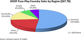
China was responsible for essentially all of the total pure-play foundry market increase in 2018. In 2019, the U.S./China trade war slowed China's economic growth but its foundry marketshare still increased by two percentage points to 21%. Moreover, despite the Covid-19 shutdown of China's economy earlier this year, China's share of the pure-play foundry market is forecast to be 22% in 2020, 17 percentage points greater than it registered in 2010 (Figure 1).

NXP Advances 5G with New Gallium Nitride Fab in Arizona

NXP Semiconductors N.V. today announced the grand opening of its 150 mm (6-inch) RF Gallium Nitride (GaN) fab in Chandler, Arizona, the most advanced fab dedicated to 5G RF power amplifiers in the United States. The new internal factory combines NXP's expertise as the industry leader in RF power and its high-volume manufacturing know-how, resulting in streamlined innovation that supports the expansion of 5G base stations and advanced communication infrastructure in the industrial, aerospace and defense markets.

COVID-19 Drives Rise in Global Fab Equipment Spending, SEMI Reports

Soaring pandemic-inspired demand for chips that power everything from communications and IT infrastructures to personal computing, gaming and healthcare electronics will drive an 8% increase in global fab equipment spending in 2020 and a 13% increase in 2021, SEMI announced today in its World Fab Forecast report. Rising demand for semiconductors for datacenter infrastructures and server storage along with the buildup of safety stock as U.S.-China trade tensions intensify are also contributing to this year's growth.

The bullish trend for overall fab equipment investments comes as the semiconductor industry recovers from a 9% decline in fab spending in 2019 and navigates a roller-coaster 2020 with actual and projected spending drops in the first and third quarters mixed with second- and fourth-quarter increases. See figure below:

GLOBALFOUNDRIES Announces 12LP+ Enhanced 12nm Silicon Fabrication Node

GLOBALFOUNDRIES (GF), the world's leading specialty foundry, today announced its most advanced FinFET solution, 12LP+, has completed technology qualification and is ready for production. GF's differentiated 12LP+ solution is optimized for artificial intelligence (AI) training and inference applications. Built on a proven platform with a robust production ecosystem, 12LP+ offers chip designers an efficient development experience and a fast time-to-market.

Contributing to its best-in-class combination of performance, power and area, 12LP+ introduces new features including an updated standard cell library, an interposer for 2.5D packaging, and a low-power 0.5 V Vmin SRAM bitcell that supports the low latency and power-efficient shuttling of data between the AI processors and memory. The result is a semiconductor solution engineered to meet the specific needs of the fast-growing AI market.

Semiconductor Fabs to Log Record Spending of Nearly $68 Billion in 2021, SEMI Reports

2021 is poised to mark a banner year for global fab equipment spending with 24 percent growth to a record US$67.7 billion, 10 percent higher than the previously forecast US$65.7 billion, and all product segments promising solid growth rates, according to the second-quarter 2020 update of the SEMI World Fab Forecast report. Memory fabs will lead worldwide semiconductor segments with US$30 billion in equipment spending, while leading-edge logic and foundry is expected to rank second with US$29 billion in investments.

The 3D NAND memory subsegment will help power the spending spree with a 30 percent jump in investments this year before tacking on 17 percent growth in 2021. DRAM fab investments will surge 50 percent next year after declining 11 percent in 2020, and fab spending on logic and foundry, mainly leading edge, will trace a similar but more muted trajectory, rising 16 percent 2021 after an 11 percent drop this year.

TSMC Says it Still Won't Build a Fab in the US

TSMC, as one of the largest silicon manufacturers in the world, has been subject to pressure from the Trump administration to build a Fab and manufacture silicon on US soil. The reasoning behind this is that the US government could order chips that are supposed to be used in military applications. For security reasons, they need to be manufactured on US grounds and "checked" by the US government. However, it seems like a Taiwanese company has no concrete plans to realize the building of the US Fab.

Thanks to the report of DigiTimes, TSMC has confirmed that they have resisted requests from the US government, and will not build a Fab on US soil for the government. They haven't dismissed the possibility of building one or silicon manufacturing facilities in the US completely. TSMC chairman Mark Liu has told DigiTimes previously that if the company wants to build a US Fab, it will do so because of consumer demand, not the government demand. And that is understandable. It is much easier to work with regular customers compared to the US government which would force a company to go through rigorous security levels to deliver chips.
TSMC HQ

TSMC Sets Aside Almost 7 Billion Dollars for Fab Expansion

TSMC is working hard to ensure its number one spot in the semiconductor manufacturing industry, and it has the funds to back it up. Yesterday TSMC's Board of Directors approved the company budget for another semiconductor fab expansion. With a budget totaling 6.74 billion US dollars allocated, TSMC has "Approved capital appropriations of approximately US$6,742.1 million (approximately NT$200.9 billion) for purposes including: 1) Fab construction, and installation of fab facility systems; 2) Installation and upgrade of advanced technology capacity; 3) Installation of specialty technology capacity; 4) Installation of advanced packaging capacity; 5) Second quarter 2020 R&D capital investments and sustaining capital expenditures."

TSMC Begins 3 nm Fab Construction

TSMC has been very aggressive with its approach to silicon manufacturing, with more investments into its R&D that now match or beat the capex investments of Intel. That indicates a strong demand for new technologies and TSMC's strong will not drop out of the never-ending race for more performance and smaller node sizes.

According to the sources over at DigiTimes, TSMC has acquired as much as 30 hectares of land in the Southern Taiwan Science Park to begin the construction of its fabs that are supposed to start high-volume manufacturing 3 nm node in 2023. Construction of 3 nm manufacturing facilities are set to begin in 2020 when TSMC will lay the groundwork for the new fab. The 3 nm semiconductor node is expected to be TSMC's third attempt at EUV lithography, right after the 7 nm+, and 5 nm nodes which are also based on EUV technology.

GLOBALFOUNDRIES Introduces 12LP+ FinFET Solution for Cloud and Edge AI Applications

GLOBALFOUNDRIES (GF), the world's leading specialty foundry, announced today at its Global Technology Conference the availability of 12LP+, an innovative new solution for AI training and inference applications. 12LP+ offers chip designers a best-in-class combination of performance, power and area, along with a set of key new features, a mature design and production ecosystem, cost-efficient development and fast time-to-market for high-growth cloud and edge AI applications.

Derived from GF's existing 12nm Leading Performance (12LP) platform, GF's new 12LP+ provides either a 20% increase in performance or a 40% reduction in power requirements over the base 12LP platform, plus a 15% improvement in logic area scaling. A key feature is a high-speed, low-power 0.5 V SRAM bit cell that supports the fast, power-efficient shuttling of data between processors and memory, an important requirement for AI applications in the computing and wired infrastructure markets.

Intel Invests €7 Billion in Ireland Toward a New Fab

Intel is following up on its massive $11 billion investment in Israel with a second large manufacturing investment, this time in Leixlip, Ireland. The company has earmarked a €7 billion investment toward construction of a new fab in Leixlip, which will employ 1,600 people, and have a built-up area of 110,000 m². This fab will sit alongside existing fabs that already employ over 4,500 staff. The company did not go into details of what the fab will manufacture. The investment aligns with Intel's strategy of massive investments in manufacturing to increase its chip volumes as enterprises, small and medium businesses, and consumers at large look to upgrade their computers at the turn of the decade. The company is already combating acute shortages of processors in the retail channel.

TSMC's 7 nm Fabrication Becomes Biggest Share of Revenue in 4Q18

TSMC's introduction of its 7 nm fabrication technology has essentially propelled the company to silicon manufacturing heights. Every company - particularly in the mobile space - is after the most minute increase in transistor density and power consumption improvements the latest and greatest can bring. AMD themselves have become a major TSMC partner in pursuit of its newfound competitiveness against Intel, and has apparently leveraged the 7 nm process as a way to keep its high-performance GPU offering minimally competitive with NVIDIA's solution - at a much lesser die area requirement, if the Radeon VII vs RTX 2080 estimates are something to go by.

As a consequence of the market interest for the 7 nm process, it has rapidly become TSMC's biggest revenue generator as soon as 4Q18. The company said that 7 nm already generated 10% of the company's entire 2018 revenue, despite the process only having been ramped up in June of the same year. Other less dense technologies still generate a lot of revenue for the company, and are likely much higher volume. However, TSMC is most likely riding on much increased ASP for 7 nm wafers than for other technologies.

Samsung, SK Hynix Slowing Down NAND, DRAM Fab Expansion Plans in Wake of Lower Demand Projections

DigiTimes is reporting plans from both Samsung and SK Hynix to slow down their fabrication capacity expansion plans for NAND and DRAM in wake of lower than expected demand projection for the first half of 2019. This move comes at a time where DRM pricing is still extremely prohibitive due to "higher demand than fabrication capacity output" - and we'd already seen the companies base their fabrication expansions on lower than expected demand increases, as a way to artificially keep pricing for the memory commodity high. NAND is another case - price per GB has been dropping like a rock. And now, the companies want to thwart expected lower demand with lower production values.

Samsung, for one, has reportedly put its plans for additional new production capacity for 1ynm DRAM chips at its fabs in Hwaseong and Pyeongtaek on hold. The chip vendor previously planned to build an additional 30,000 wafers monthly for DRAM memory starting the third quarter of 2018, the sources said - but is now looking to reduce that number to keep pricing from bottoming out. Sk Hynix is also reported to have slowed down its projected production, but details are scarcer on that side of the fence. All in all, it seems that whether there is demand or not, seeing DRAM prices falling to their previous levels is a dream in both name and, not paradoxically, reality.

TSMC Approves $4.5B investment in R&D, Fabrication Development

TSMC's Board of Directors convened yesterday with the intention of defining the company's strategy for future developments and investment. The result was a commitment of $4.5B to investments ranging from construction of fab facilities; installation, expansion, and upgrade of advanced technology capacity; conversion of logic capacity to specialty technology capacity; conversion of mature technology capacity to specialty technology capacity; expansion and upgrade of specialty technology capacity; expansion of advanced packaging technology capacity; and fourth quarter 2018 R&D capital investments and sustaining capital expenditures. These values pale in comparison to Samsung's usual investment applications, of course; but let's not forget is an industry behemoth with more product lines and investment opportunities that TSMC's comparably "specific" domain of the market.

Samsung to Invest $27.7 billion On Second Pyeongtaek Semiconductor Plant

Samsung's management committee has reportedly convened this morning, February 7th, to officially approve an investment plan on a new semicondctor manufacturing facility. Reports say this new factory is expected to be built on Pyeongtaek, the same general location as Samsung's current Pyeongtaek Fab 1. The investment plan is being made with plans for the plant to start production of the "P2-Project" plant during the first half of 2019.

Giving credence to these industry reports is the fact that Samsung has already celebrate gas pipeline contracts with companies (such as Wonik Holdings), just last month, in preparation for this new fab construction. It's as of yet unclear what specific plan the company has for the new factory, though it will certainly inject extraordinary new amounts of volume to Samsung's various foundry businesses. With two years of construction since it broke ground in May, 2015, the original fabrication line at the Pyeongtaek campus is currently the largest single Fab in the industry; in the face of this, it seems that a "first half of 2019" starting date for semiconductor production at Samsung's new manufacturing facilities may be slightly optimistic. However, those plans start to sound a little more on the doable side if one considers these might actually be plans for an expansion of the current Pyeongtaek Fab 1 facilities, plans for which the company has already announced back in July 2017.

TSMC Breaks Ground on 5nm 'Fab 18' in Taiwan

TSMC today held a groundbreaking ceremony for its Fab 18, Phase 1 facility at the Southern Taiwan Science Park. Led by Chairman Dr. Morris Chang, the event demonstrates TSMC's ongoing commitment to investing in Taiwan as well as to environmental sustainability, and marks another milestone in TSMC's 30-year history and its competitive advantage in technology leadership, manufacturing excellence, and customer trust. TSMC's Fab 18 will be its fourth 12-inch GigaFab in Taiwan and is scheduled for production of the advanced 5 nanometer process.

Following today's groundbreaking, the Company plans to complete construction of Phase 1 and begin equipment move-in in the first quarter of 2019, with volume production in early 2020. Phase 2 will start construction in third quarter 2018 and also enter volume production in 2020, while Phase 3 construction is scheduled for third quarter 2019 for volume production in 2021. Once all three phases enter production, the facility's estimated annual capacity will exceed one million 12-inch wafers, providing 4,000 high-quality jobs and becoming another bastion of TSMC's manufacturing excellence.

Toshiba to Prepare New Semiconductor Fabrication Facility in ¥7b Investment

Toshiba Corporation today announced that it is going ahead with a forward-looking plan for a new memory fabrication facility in Kitakami, Iwate prefecture. Toshiba Memory Corporation (TMC), a wholly owned subsidiary of Toshiba, will establish a company to operate the facility, and invest approximately 7 billion yen in site preparation and initial construction work in FY2017. The new facility, announced on September 6, 2017, will produce BiCS Flash, TMC's proprietary flash memory. It will be TMC's seventh fab.
Return to Keyword Browsing
May 21st, 2024 15:42 EDT change timezone

New Forum Posts

Popular Reviews

Controversial News Posts