News Posts matching #Flash Memory

Return to Keyword Browsing

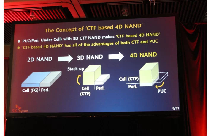
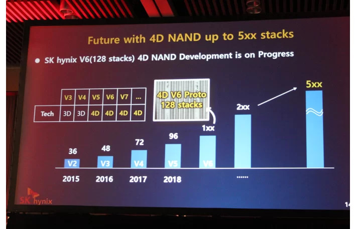
Yangtze Memory Begins Mass-production of 64-layer 3D NAND Flash Memory

Yangtze Memory Technologies (YMTC), a Chinese state-backed semiconductor company founded in 2016 as part of the Chinese Government's tech-independence push, has commenced mass-production of 64-layer 3D NAND flash memory chips, at a rate of 100,000 to 150,000 wafers per month leading into 2020. The 64-layer 3D NAND chips are based on YMTC's "in-house" Xtracking architecture. The company is already developing a 128-layer 3D NAND flash chip, and is skipping 96-layer along the way.

YMTC's capacity will be augmented by a new fab being built by its parent company, Tsinghua Unigroup. Tsinghua is a state-owned company which holds a controlling 51 percent stake in YMTC, and is a beneficiary of China's National Semiconductor Industry Investment Fund. When it goes online in 2021-22, the new Tsinghua fab, located in Chengdu, will augment YMTC's capacity by an additional 100,000 12-inch wafers per month. Its existing fab in Nanjing will also receive a capacity expansion.

Toshiba Talks About 5-Bit-per-Cell (PLC) Flash Memory

Toshiba at the Flash Memory Summit announced they've managed to develop a 5-Bit-per-Cell memory solution Based on its BiCS 4 flash memory technologies, the feat was achieved using a modified module of Quad-Level Cell (QLC) memory. This shows the technology is not only feasible, but has room for improvement, since an adapted QLC technology will always be inferior to a natively-developed, Penta-Level Cell (PLC) solution.

To achieve this ability to store one extra bit of information per cell (compared to QLC), a new level of voltage refinement is required: the cell has to be able to change its state according to one of 32 voltage states, which, in turn, have to be read out correctly by the flash memory controller. This reduces the cell's performance and endurance (as does any increase in the number of bits per cell), and will require a number of solutions to mitigate and compensate for this reduced performance. However, density has become an increasing concern from manufacturers, hence the continued development of deeper, more variable voltage states that allow for even more information to be stored in the same silicon area. Higher density means cheaper solutions, but density increased in such a way has known trade-offs that have been much talked about ever since the transition from Single-Level Cell (SLC) up to the (nowadays ubiquitous) QLC.

Realtek Announces New Flash Controllers, Including one for PCIe Gen 4 NVMe SSDs

At the 2019 Flash Memory Summit, Realtek announced a slew of new Flash memory controllers targeting a diversity of devices, spanning from USB flash drives to USB external SSDs, M.2/U.2 NVMe internal SSDs. Leading the pack is the RTS5771, the company's new flagship NVMe SSD controller that features a PCI-Express 4.0 x4 host interface, 8 NAND Flash channels with up to 1,200 MT/s speeds per channel, NVMe 1.3, and DRAM cache. This becomes the third PCIe gen 4.0-capable client-segment NVMe SSD controller after the Phison E16 and the Marvell 88SS132x.

The RTS5765DL is its cost-effective sibling, which has PCI-Express 3.0 x4 host interface, just 4 NAND Flash channels, and is DRAM-less, allowing manufacturers to design cost-effective SSDs. It still has 1,200 MT/s bandwidth per channel, so drives that implement it can offer sequential speeds similar to premium drives from the previous generation. The new RTL9210 is a bridge chip that converts USB 3.1 gen 2 (10 Gbps) to PCI-Express 3.0 x2, ideal for cost-effective external NVMe SSDs. The controller also features an integrated RGB LED logic, so drive designers can bling up their creations.

SANBlaze Presents PCIe NVMe Gen4 at Flash Memory Summit

SANBlaze Technology, Inc., a leader in NVMe test platforms and Storage Emulation systems, announced today that it is demonstrating its new state-of-the-art PCIe NVMe Gen4 Test System, the SANBlaze SBExpress-RM4 at FMS, providing NVMe SSD manufacturers performance and compliance testing on their NVMe solid state storage drives. As early adopters, major manufacturers of NVMe Gen4 SSDs have qualified SANBlaze's Gen4 offering, and the company is now excited to announce general availability of their Gen4 solution during FMS

Gen4, the next generation of PCIe (PCIe 4.0) doubles the bandwidth from 1 GB/s to 2 GB/s per lane while providing better signal reliability and integrity for improved performance. With PCIe Gen4 providing the fastest interconnect speeds to date, the SANBlaze SBExpress has now doubled its bandwidth from 16GB to 32GB per host adapter.

"PCIe Gen4 technology is here, and it's perfectly matched to the next generation of storage that NVMe Gen4 drives offer. PCIe Gen4 doubles the bandwidth of the storage interconnect and keeps NVMe well ahead of any competing technology," said Vince Asbridge, President of SANBlaze. "Gen4 also introduces a significant set of challenges to drive manufacturers in terms of qualification infrastructure. Our state-of-the-art SBExpress-RM4 system allows connectivity of up to 16 NVMe Gen4 drives, single or dual path, allowing drive manufacturers to qualify NVMe Gen4 drives at PCIe Gen4 speeds using our Certified by SANBlaze suite of automated tests."

ATP Shows Off Next-Generation Industrial Only Flash Solutions at FMS 2019

Triple level cell (TLC) flash, long considered for consumer applications only, is now making inroads into rigid industrial segments where reliable performance and extended endurance are essential. 3D TLC-based flash solutions are among the next-generation products that ATP Electronics will showcase during the 2019 Flash Memory Summit at the Santa Clara Convention Center in California, USA from August 6 to 8 in meeting room #205. ATP is the leading manufacturer of "Industrial Only" memory and storage solutions committed to delivering the best total cost of ownership (TCO) value through longevity support, extensive testing and screening, and uncompromising quality.

"As an industrial only manufacturer, ATP is dedicated to making sure that our customers get the most out of their TCO. We take pride in having full in-house ownership of the manufacturing process, which allows us greater flexibility to meet customer needs and guarantee superior quality. With ATP NAND packaging and stringent testing capabilities, we guarantee the NAND quality control of our own-built modules to deliver extended lifespan and longevity support even after other manufacturers have stopped making products for legacy systems," said Marco Mezger, ATP Vice President of Global Marketing.

SK Hynix Begins Sampling 96-layer 4D QLC NAND Flash Memory

SK Hynix Inc., announced today that it has delivered samples of new 1Tb (Terabit) QLC (Quadruple Level Cell) product to major SSD (Solid State Drive) Controller companies. The Company applied its own QLC technology to its world's first 96-Layer "CTF (Charge Trap Flash) based 4D (Four-Dimensional) NAND Flash (or 4D NAND)." SK Hynix intends to expand its NAND portfolio to 96-layer-based 1Tb QLC products in time for the QLC market opening and strengthen its responsiveness to the next-generation high-density memory market.

QLC stores four bits of data in one NAND cell, allowing higher density compared to TLC (Triple Level Cell) that stores three bits per cell. Using QLC, it is possible to develop high-density products with cost competitiveness. SK Hynix is able to secure the industry's top-level cost competitiveness through this product, which has reduced the area to less than 90% of the existing 3D-based QLC products.

Toshiba Memory Unveils 1TB Single Package PCIe Gen3 x4 SSD with 96-Layer 3D Flash

Toshiba Memory Corporation, the world leader in memory solutions, today announced the BG4 series, a new line-up of single package NVMe SSDs with capacities up to 1,024 GB, which places both innovative 96-layer 3D flash memory and an all-new controller into one package to deliver best-in-class read performance. The BG4 series is currently sampling to PC OEM customers in limited quantities, with general sample availability expected later in the second calendar quarter of 2019.

This new series of single package SSDs, featuring PCIe Gen 3.0 x4 lanes, offers sequential read performance up to 2,250 MB/s, and with improved flash management delivers industry-leading random read performance up to 380,000 IOPS. The BG4 single package SSDs are suitable for compact and performance-oriented systems, such as ultra-thin PC notebooks, IoT embedded systems and server boot in data centers.

Lite-On Unveils Powerful New SSD for Enterprise Workloads

At the Flash Memory Summit (FMS) 2018, LITE-ON Storage previewed the first EDSFF 1U solid-state drive (SSD) to emerge from its work with CNEX Labs. The revolutionary drive gained great interest among storage advocates.

In collaboration with such partners, LITE-ON delivers an innovative and highly efficient storage solution for scalable computing that aligns to Open Compute Project (OCP) specifications. The resulting EDSFF (Enterprise and Datacenter SSD Form Factor) SSD will provide a more cost-effective solution for enterprise and hyperscale cloud environments.

"Standard SSD solutions are great at handling many typical business workloads, but the complexity of storing information in both cloud and data center infrastructure requires SSD firmware to be flexible and adaptable," said Charlie Tseng, CEO of LITE-ON Storage. "LITE-ON's expertise in SSD firmware is perfect for the varying needs of customers."

NAND Flash Prices Could Reach $0.08/GB in 2019

Prices of NAND flash could drop to historic lows of $0.08 per gigabyte in 2019, according to Jim Handy from Objective Analysis, addressing delegates at the 2018 Flash Memory Summit. If you add the cost of the controller, optional DRAM chip, and other low-cost parts that make up an SSD, 480~512 GB drives under $70 could finally be a reality; followed by 1 TB under $120, and 2 TB under $200. Handy attributes the low prices to a catastrophic oversupply of NAND flash in the industry, which could push manufacturers to the brink of economic collapse.

The price drop is also accelerated with the introduction of the QLC (4 bits per cell) technology, which increases densities (and conversely decreases price/GB). Luckily, most NAND flash manufacturers also happen to make DRAM, and are offsetting some of their NAND flash losses with DRAM profits, as DRAM remains in undersupply. The NAND flash price-crash threatens to wipe out conventional hard-disk drives from the consumer-space, at least in matured markets; relegating them to developing markets.

SK Hynix Unveils 4D NAND Flash Memory Concept

3D NAND flash revolutionized flash storage as it used the third dimension (height) to stack multiple NAND flash layers, resulting in infinitesimally smaller footprint and reduced costs. SK Hynix believes that a "4-dimensional" NAND flash package is possible. Don't worry, such a stack doesn't look like a tesseract. Conventional 3D NAND flash relies on stacks of charge-trap flash (CTF) cells spatially located alongside its periphery block (which is responsible for wiring out each of the layers of the CTF stack). On a 2-D plane you'd be spending substrate real-estate on both the CTF and periphery block.

SK Hynix believes that the periphery block can be stacked along with the CTF stack, with microscopic vias wiring up the stack along the periphery, reducing the footprint of each cell stack. 4D stacking will also allow for greater number of CTF stacks per cell. Just to be clear, we're talking about stacks of cell and not stacks of NAND flash dies. The V5 cell-stack in SK Hynix's design entails 4 cells and periphery blocks sandwiched. The first implementation of this technology is a 96-layer 4D NAND flash chip with 512 Gb of capacity and TLC (3 bits per cell) density, although the technology is ready for QLC cells. This 512 Gb chip will begin sampling by the end of 2018, and the company is already working on a 1 Tb chip for 2019.

Yangtze Memory Technologies to Debut New, Ultra-Fast 3D NAND Architecture and Deliver Keynote at Flash Memory Summit 2018

Yangtze Memory Technologies Co., Ltd (YMTC), a new player in the NAND industry, will be joining Flash Memory Summit this year for the first time, delivering a much-anticipated keynote address to reveal its ground-breaking technology - Xtacking. YMTC is the first Chinese company to take part in the high-entry-barrier NAND flash memory industry with its new architecture for unprecedented performance, higher bit density, and faster time-to-market.

Simon Yang, YMTC CEO, will deliver a keynote address, Unleashing 3D NAND's Potential with an Innovative Architecture, on August 7th, from 3:00 p.m. at the Mission Ballroom in the Santa Clara Convention Center, where he will illustrate how the company's new technology can increase NAND I/O speed up to DRAM DDR4 while delivering industry-leading bit density, marking a quantum leap for the NAND market.

ATP Miniature Storage Powerhouses Take Center Stage at FMS 2018

The volume of data traffic is growing by the minute, and ATP Electronics, a leading manufacturer of high-performance industrial memory and storage solutions, is meeting colossal storage demands with its latest portfolio built for space-restricted embedded, industrial, and automotive systems. ATP shows off its extensive array of flash memory and storage products at the Flash Memory Summit 2018 in Sta. Clara, USA from August 7 to 9.

"We are seeing data propelling the transformation of cities and nations, and we need effective solutions of handling, storing and analyzing data to deliver rapid, actionable insights that will improve the way we live and do business," noted Marco Mezger, ATP Vice President of Global Marketing. "As the Internet of Things (IoT) adoption gains momentum, systems are diminishing in size so memory and storage solutions have to adapt. ATP is thoroughly amplifying reliability, endurance, performance and capacity in its embedded and removable flash products while keeping them compact and portable," he added.

Toshiba Develops 96-layer BiCS FLASH with QLC Technology

Toshiba Memory Corporation, the world leader in memory solutions, today announced that it has developed a prototype sample of 96-layer BiCS FLASH, its proprietary 3D flash memory, with 4-bit-per-cell (quad level cell, QLC) technology that boosts single-chip memory capacity to the highest level yet achieved.Toshiba Memory will start to deliver samples to SSD and SSD controller manufacturers for evaluation from the beginning of September, and expects to start mass production in 2019.

The advantage of QLC technology is pushing the bit count for data per memory cell from three to four and significantly expanding capacity. The new product achieves the industry's maximum capacity of 1.33 terabits for a single chip which was jointly developed with Western Digital Corporation. This also realizes an unparalleled capacity of 2.66 terabytes with a 16-chip stacked architecture in one package. The huge volumes of data generated by mobile terminals and the like continue to increase with the spread of SNS and progress in IoT, and the need to analyze and utilize that data in real time is expected to increase dramatically. That will require even faster than HDD, larger capacity storage and QLC products using the 96-layer process will contribute a solution.

Toshiba Memory Corporation to Expand 3D Flash Memory Production Capacity

Toshiba Memory Corporation (TMC) today announced that it decided to start construction of a new state-of-the-art fab for BiCS FLASH , its proprietary 3D flash memory, in Kitakami, Iwate prefecture in July this year.

TMC has selected Kitakami City as the next location to expand its operations in September last year, and has started preparations for construction of the new fab. Demand for 3D flash memory is increasing significantly on fast growing demand for enterprise SSD for datacenters and servers. TMC expects continued strong growth in the mid and long term, and the timing of its construction positions it to capture this growth and expand its business.

The new fab will be completed in 2019, and will have a quake absorbing structure and an environmentally friendly design that includes the latest energy saving manufacturing equipment. It will also introduce an advanced production system that uses artificial intelligence (AI) to boost productivity. Decisions on the new fab's equipment investment, production capacity and production plan will reflect market trends. TMC expects to continue its joint venture investments based on discussion with Western Digital in the new facility.

Intel Reimagines Data Center Storage with New 3D NAND SSDs

Today, Intel announced the Intel SSD DC P4510 Series for data center applications. The P4510 Series uses 64-layer TLC Intel 3D NAND to enable end users to do more per server, support broader workloads and deliver space-efficient capacity. The P4510 Series enables up to four times more terabytes per server and delivers up to 10 times better random read latency at 99.99 percent quality of service than previous generations. The drive can also deliver up to double the input-output operations per second (IOPS) per terabyte. The 1 and 2TB capacities have been shipping to cloud service providers (CSPs) in high volume since August 2017, and the 4 and 8TB capacities are now available to CSPs and channel customers. All capacities are in the 2.5-inch 15 mm U.2 form factor and utilize a PCIe NVMe 3.0 x4 connection.

To accelerate performance and simplify management of the P4510 Series PCIe SSDs and other PCIe SSDs, Intel is also delivering two new technologies that work together to replace legacy storage hardware. Intel Xeon Scalable processors include Intel Volume Management Device (VMD), enabling robust management such as surprise insertion/removal and LED management of PCIe SSDs directly connected to the CPU. Building on this functionality, Intel Virtual RAID on CPU (VROC) uses Intel VMD to provide RAID to PCIe SSDs. By replacing RAID cards with Intel VROC, customers are able to enjoy up to twice the IOPs performance and up to a 70 percent cost savings with PCIe SSDs directly attached to the CPU, improving customer's return on their investments in SSD-based storage.

Toshiba Unveils Embedded NAND Flash Memory Products for Automotive Applications

Toshiba Memory Corporation, the world leader in memory solutions, today announced that it has begun shipping samples of embedded NAND flash memory products for automotive applications that are compliant with JEDEC UFS version 2.1. The new products meet AEC-Q100 Grade2 requirements and support a wide temperature range of -40°C to +105°C, offering the enhanced reliability capabilities that are required by increasingly complex automotive applications. The line-up meets a broad range of applications requirements with five different capacities: 16 GB, 32 GB, 64 GB, 128 GB and 256 GB.

The new products are embedded NAND flash memory products that integrate NAND chips fabricated with 15 nm process technology and a controller in a single package. Storage requirements for automotive applications continue to increase as systems including automotive information & entertainment systems and ADAS become more sophisticated, and UFS supports their high performance and density needs. The addition of automotive UFS expands Toshiba Memory Corporation's line-up of embedded NAND flash memory products for automotive applications, which currently includes automotive e-MMC products. Utilizing the UFS interface allows the new products to achieve sequential read of 850 MB/s and random read of 50,000 IOPS, which are approximately 2.7 times and 7.1 times faster than their current e-MMC counterparts, respectively.

Samsung Readies 970 and 980 Series NVMe SSDs

At its Flash Memory Summit booth, Samsung revealed plans to launch new consumer-segment SSDs which succeed its current 960 EVO and 960 Pro series. Over 2017-18, the company is expected to launch the new 970 series and 980 series NVMe SSDs. Tom's Hardware predicts that Samsung could dispose of the "EVO" and "Pro" brand extensions to a static model number (such as 960 or 950). Samsung could tap into its current 3-bit per cell (TLC) 64-layer 3D V-NAND flash memory for the 970 and 980 series. With the company busy capacity-building for 4-bit per cell (QLC), the new SSD lines may not feature it, although Samsung is capable of surprising with aggressive launch cycles. As drives supporting the NVMe protocol, the 970 and 980 series could ship in modern form-factors, such as M.2 and U.2.

Samsung Introduces Far-reaching V-NAND Memory Solutions

Samsung Electronics, the world leader in advanced memory technology, has announced new V-NAND (Vertical NAND) memory solutions and technology that will address the pressing requirements of next-generation data processing and storage systems. With the rapid increase of data-intensive applications across many industries using artificial intelligence and Internet of Things (IoT) technologies, the role of flash memory has become extremely critical in accelerating the speed at which information can be extracted for real-time analysis.

At the inaugural Samsung Tech Day and this year's Flash Memory Summit, Samsung is showcasing solutions to address next-generation data processing challenges centered around the company's latest V-NAND technology and an array of solid state drives (SSDs). These solutions will be at the forefront of enabling today's most data-intensive tasks such as high-performance computing, machine learning, real-time analytics and parallel computing.

Toshiba Announces SG6 Series SATA Client SSD Utilizing 64-Layer 3D Flash

Toshiba Memory Corporation, the world leader in memory solutions, today announced the launch of the SG6 series, a new line-up of SATA client SSDs utilizing Toshiba Memory Corporation's cutting-edge 64-layer, 3-bit-per-cell (TLC) BiCS FLASH. Sample shipments to PC OEM customers start today in limited quantities, and Toshiba Memory Corporation will gradually increase shipments from the fourth calendar quarter of this year.

The new SG6 series SSDs features a SATA Revision 3.3, 6.0Gbit/s interface, and delivers performance of up to 550MB/s sequential read and 535MB/s sequential write. Thanks to improved flash memory management and performance, active power consumption is cut by approximately 40% compared to previous generation products. This improvement can extend battery life, a plus for many applications including mobile computing.

Intel Further Delivers on Storage Transformation with New SSD Form Factor

Today, Intel announces major data center storage advances, reiterating Intel's memory technology leadership. The new technologies advance data center storage and deliver innovative solutions to meet the challenges presented by the growing reliance on data. They include:
  • "Ruler" form factor for Intel SSDs, an all-new solid state drive form factor enabling up to 1PB of storage in a 1U server rack in the future.
  • The world's most advanced dual port portfolio: Intel Optane technology dual port SSDs and Intel 3D NAND dual port SSDs for mission-critical applications.
  • An updated SATA family of SSDs for data center, targeted at HDD replacement.
"We are in the midst of an era of major data center transformation, driven by Intel. These new "ruler" form factor SSDs and dual port SSDs are the latest in a long line of innovations we've brought to market to make storing and accessing data easier and faster, while delivering more value to customers," said Bill Leszinske, Intel vice president, Non-Volatile Memory Solutions Group (NSG), and director, strategic planning, marketing and business development. "Data drives everything we do - from financial decisions to virtual reality gaming, and from autonomous driving to machine learning - and Intel storage innovations like these ensure incredibly quick, reliable access to that data."

Toshiba Introduces World's First Enterprise-Class SSDs with 64-Layer 3D Flash Me

Toshiba America Electronic Components, Inc. (TAEC), a committed technology leader, today unveiled the development of two new flagship enterprise solid state drive (SSD) solutions, the TMC PM5 12 Gbit/s SAS series and the CM5 NVM Express (NVMe) series. Development is expected to be completed in the fourth quarter. Both product lines are built with TMC's latest 64 layer, 3-bit-per-cell enterprise-class TLC (triple-level cell) BiCS FLASH2, making it possible for today's demanding storage environments to expand the use of flash with cost-optimized 3D flash memory. With all-new, advanced features, the innovative CM5 and PM5 series raise the bar in performance capabilities and create new opportunities for businesses to leverage the power of flash storage.

Offering up to 30.72TB in a 2.5-inch form factor, the TMC PM5 series introduces a full range of endurance and capacity SAS SSDs enabling data centers to effectively address big data demands while streamlining storage deployments. With the industry's first MultiLink SAS architecture, the PM5 series is able to deliver the fastest performance the market has seen from a SAS-based SSD with up to 3,350 MB/s of sequential read and 2,720 MB/s of sequential write6 in MultiLink mode and up to 400,000 random read IOPS in narrow or MultiLink mode. The PM5 series' 4-port MultiLink design is an additional technology to achieve high performance, close to PCI EXPRESS (PCIe)8 SSDs, enabling legacy infrastructures to increase productivity without having to be re-architected from the ground up. Furthermore, PM5 SSDs support multi-stream write technology, a feature that intelligently manages and groups data types to minimize write amplification and minimize garbage collection, translating into reduced latency, improved endurance, increased performance and Quality of Service (QoS).

Western Digital Announces Four-Bits-Per-Cell (X4) Technology on 3D NAND

Western Digital Corp. today announced its successful development of four bits per cell, X4, flash memory architecture offering on 64-layer 3D NAND, BiCS3, technology. Building on its pioneering innovation of X4 for 2D NAND technology and past success in commercializing it, the company has now developed X4 for 3D NAND by leveraging its deep vertical integration capabilities. These include silicon wafer processing, device engineering to provide sixteen distinct data levels in every storage node, and system expertise for overall flash management. BiCS3 X4 technology delivers an industry-leading storage capacity of 768 gigabits on a single chip, a 50 percent increase from the prior 512 gigabit chip that was enabled with the three bits per cell (X3) architecture. Western Digital will showcase removable products and solid-state drives built with BiCS3 X4 and systems capabilities in August at the Flash Memory Summit in Santa Clara, California.

"The implementation of X4 architecture on BiCS3 is a significant development for Western Digital as it demonstrates our continued leadership in NAND flash technology, and it also enables us to offer an expanded choice of storage solutions for our customers," said Dr. Siva Sivaram, executive vice president, Memory Technology, Western Digital. "The most striking aspect in today's announcement is the use of innovative techniques in the X4 architecture that allows our BiCS3 X4 to deliver performance attributes comparable to those in BiCS3 X3. The narrowing of the performance gap between the X4 and X3 architectures is an important and differentiating capability for us, and it should help drive broader market acceptance of X4 technology over the next several years."

Toshiba Develops World's First 3D Flash Memory with TSV Technology

Toshiba Memory Corporation, the world leader in memory solutions, today announced development of the world's first BiCS FLASH three-dimensional (3D) flash memory utilizing Through Silicon Via (TSV) technology with 3-bit-per-cell (triple-level cell, TLC) technology. Shipments of prototypes for development purposes started in June, and product samples are scheduled for release in the second half of 2017. The prototype of this groundbreaking device will be showcased at the 2017 Flash Memory Summit in Santa Clara, California, United States, from August 7-10.

Devices fabricated with TSV technology have vertical electrodes and vias that pass through silicon dies to provide connections, an architecture that realizes high speed data input and output while reducing power consumption. Real-world performance has been proven previously, with the introduction of Toshiba's 2D NAND Flash memory.

Toshiba Develops World's First 4-bit Per Cell QLC NAND Flash Memory

Toshiba America Electronic Components, Inc. (TAEC) today announced the latest generation of its BiCS FLASH three-dimensional (3D) flash memory. The newest BiCS FLASH device features 4-bit-per-cell, quadruple-level cell (QLC) technology and is the first 3D flash memory device to do so. Toshiba's QLC technology enables larger (768 gigabit) die capacity than the company's third-generation 512Gb 3-bit-per-cell, triple-level cell (TLC), and pushes the boundaries of flash memory technology.

Toshiba's new QLC BiCS FLASH device features a 64-layer stacked cell structure and achieves the world's largest die capacity (768Gb/96GB). QLC flash memory also enables a 1.5-terabyte (TB) device with a 16-die stacked architecture in a single package - featuring the industry's largest capacity. This is a fifty percent increase in capacity per package when compared to Toshiba's earlier announcement of a 1TB device with a 16-die stacked architecture in a single package - which also offered the largest capacity in the industry at the time.

Toshiba Now Shipping Samples of 64-Layer, 512-gigabit 3D Flash Memory

Toshiba Corporation has today unveiled the latest addition in its industry-leading line-up of BiCS FLASH three-dimensional flash memory with a stacked cell structure, a 64-layer device that achieves a 512-gigabit (64-gigabytes) capacity with 3-bit-per-cell (triple-level cell, TLC) technology. The new device will be used in applications that include enterprise and consumer SSD. Sample shipments of the chip started this month, and mass production is scheduled for the second half of this calendar year.

Toshiba continues to refine BiCS FLASH, and the next milestone on its development roadmap is the industry's largest capacity, a 1-terabyte product with a 16-die stacked architecture in a single package. Plans call for the start of sample shipments in April 2017. For the new 512-gigabit device, Toshiba deployed leading-edge 64-layer stacking process to realize a 65% larger capacity per unit chip size than the 48-layer 256-gigabit (32-gigabytes) device, and has increased memory capacity per silicon wafer, reducing the cost per bit.
Return to Keyword Browsing
May 21st, 2024 16:01 EDT change timezone

New Forum Posts

Popular Reviews

Controversial News Posts