News Posts matching #GDDR5X

Return to Keyword Browsing

Mid-range "Pascal" GPUs Stick to GDDR5-class Memory

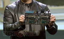
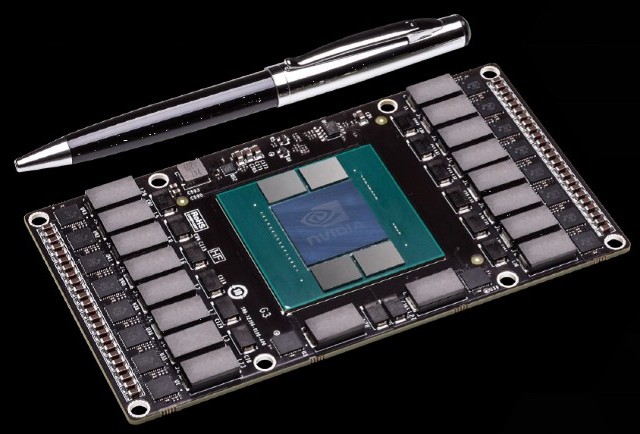
At the NVIDIA Drive PX compute module unveiling, company CEO Jen-Hsun Huang gave us the first glimpse of a mid-range GPU based on the "Pascal" architecture. This chip looks a lot more conventional than the fancy HBM2-infused multi-chip module that's at the heart of the Tesla P100. Its package is a traditional green fiberglass substrate with a rectangular die at the center; and is surrounded by conventional-looking GDDR5-class memory chips (which could very well be GDDR5X). The Drive PX is a GPU-accelerated deep-learning box that NVIDIA is basing much of its self-driving car tech around; and uses a pair of these mid-range "Pascal" MXM boards.

AMD "Greenland" Vega10 Silicon Features 4096 Stream Processors?

The LinkedIn profile of an R&D manager at AMD discloses key details of the company's upcoming "Greenland" graphics processor, which is also codenamed Vega10. Slated for an early-2017 launch, according to AMD's GPU architecture roadmap, "Greenland" will be built on AMD's "Vega" GPU architecture, which succeeds even the "Polaris" architecture, which is slated for later this year.

The LinkedIn profile of Yu Zheng, an R&D manager at AMD (now redacted), screencaptured by 3DCenter.org, reveals the "shader processor" (stream processor) count of Vega10 to be 4,096. This may look identical to the SP count of "Fiji," but one must take into account "Greenland" being two generations of Graphics CoreNext tech ahead of "Fiji," and that the roadmap slide hints at HBM2 memory, which could be faster. One must take into account AMD's claims of a 2.5X leap in performance-per-Watt over the current architecture with Polaris, so Vega could only be even faster.

Micron Begins Sampling GDDR5X Memory to Customers

DRAM and NAND flash giant Micron Technology has begun sampling its next-generation GDDR5X memory chips to customers. The company is ready with chips in the 8 Gb (1 GB) and 16 Gb (2 GB) densities, making it possible for GPU makers to build graphics cards with 8 GB and 16 GB total onboard memory, respectively, over a 256-bit wide memory bus, by using just one chip per 32-bit channel.

Apart from 8 Gb and 16 Gb densities, Micron's GDDR5X chips offer GPU makers a transition from GDDR5 with minimal engineering, since the standard has similar electricals to its predecessor, and a similar BOM structure; while offering up to double the clock speeds to GDDR5, and running at a lower voltage of 1.35V. Both AMD and NVIDIA have reportedly expressed interest in building graphics cards with GDDR5X.

NVIDIA's Next Flagship Graphics Cards will be the GeForce X80 Series

With the GeForce GTX 900 series, NVIDIA has exhausted its GeForce GTX nomenclature, according to a sensational scoop from the rumor mill. Instead of going with the GTX 1000 series that has one digit too many, the company is turning the page on the GeForce GTX brand altogether. The company's next-generation high-end graphics card series will be the GeForce X80 series. Based on the performance-segment "GP104" and high-end "GP100" chips, the GeForce X80 series will consist of the performance-segment GeForce X80, the high-end GeForce X80 Ti, and the enthusiast-segment GeForce X80 TITAN.

Based on the "Pascal" architecture, the GP104 silicon is expected to feature as many as 4,096 CUDA cores. It will also feature 256 TMUs, 128 ROPs, and a GDDR5X memory interface, with 384 GB/s memory bandwidth. 6 GB could be the standard memory amount. Its texture- and pixel-fillrates are rated to be 33% higher than those of the GM200-based GeForce GTX TITAN X. The GP104 chip will be built on the 16 nm FinFET process. The TDP of this chip is rated at 175W.

AMD Unveils GPU Architecture Roadmap, "Polaris" to Skip HBM2 Memory?

Alongside its big Radeon Pro Duo flagship graphics card launch, AMD unveiled its GPU architecture roadmap that looks as far into the future as early-2018. By then, AMD will have launched as many as three new GPU architectures. It begins with the launch of its 4th generation Graphics CoreNext architecture, codenamed "Polaris," in mid-2016. Built on the 14 nm FinFET process, "Polaris" is expected to offer a whopping 2.5x increase in performance-per-Watt for AMD, compared to its current GCN 1.2 architecture on 28 nm.

Hot on Polaris' heels, in early-2017, AMD plans to launch the "Vega" GPU architecture. While this appears to offer a 50% increase in performance-per-Watt over Polaris, its highlight is HBM2 memory. Does this mean that AMD plans to skip HBM2 on Polaris, and stick to GDDR5X? Could AMD be opting for a similar approach to NVIDIA, by launching its performance-segment GPU first as an enthusiast product, giving it a free run on the markets till early-2017, and then launching a Vega-based big-chip with HBM2 memory, taking over as the enthusiast-segment product? Some time in early-2018, AMD will launch the "Navi" architecture, which appears to offer a 2.5x performance-per-Watt lead over Polaris, taking advantage of an even newer memory standard.

NVIDIA "GP104" Silicon to Feature GDDR5X Memory Interface

It looks like NVIDIA's next GPU architecture launch will play out much like its previous two generations - launching the second biggest chip first, as a well-priced "enthusiast" SKU that outperforms the previous-generation enthusiast product, and launching the biggest chip later, as the high-end enthusiast product. The second-biggest chip based on NVIDIA's upcoming "Pascal" architecture, the "GP104," which could let NVIDIA win crucial $550 and $350 price-points, will be a lean machine. NVIDIA will design the chip to keep manufacturing costs low enough to score big in price-performance, and a potential price-war with AMD.

As part of its efforts to keep GP104 as cost-effective as possible, NVIDIA could give exotic new tech such as HBM2 memory a skip, and go with GDDR5X. Implementing GDDR5X could be straightforward and cost-effective for NVIDIA, given that it's implemented the nearly-identical GDDR5 standard on three previous generations. The new standard will double densities, and one could expect NVIDIA to build its GP104-based products with 8 GB of standard memory amounts. GDDR5X breathed a new lease of life to GDDR5, which had seen its clock speeds plateau around 7 Gbps/pin. The new standard could come in speeds of up to 10 Gbps at first, and eventually 12 Gbps and 14 Gbps. NVIDIA could reserve HBM2 for its biggest "Pascal" chip, on which it could launch its next TITAN product.

SK Hynix to Ship 4GB HBM2 Stacks by Q3-2016

Korean DRAM and NAND flash giant SK Hynix will be ready to ship its 4 GB stacked second generation high-bandwidth memory (HBM2) chips from Q3, 2016. These packages will be made up of four 1 GB dies, with a bandwidth-per-pin of 1 Gbps, 1.6 Gbps, and 2 Gbps, working out to per-stack bandwidths of 128 GB/s, 204 GB/s, and 256 GB/s, respectively.

These chips will target applications such as graphics cards, network infrastructure, HPC, and servers. The company is also designing 8 GB stacks, made up of eight 1 GB dies. These stacks will be targeted at HPC and server applications. The company is also offering cost-effective 2 GB, 2-die stacks, for graphics cards. The cost-effective 2 GB, 2-die stacks could prove particularly important for the standard's competition against GDDR5X, particularly in mid-range and performance-segment graphics cards.

NVIDIA GP100 Silicon to Feature 4 TFLOPs DPFP Performance

NVIDIA's upcoming flagship GPU based on its next-generation "Pascal" architecture, codenamed GP100, is shaping up to be a number-crunching monster. According to a leaked slide by an NVIDIA research fellow, the company is designing the chip to serve up double-precision floating-point (DPFP) performance as high as 4 TFLOP/s, a 3-fold increase from the 1.31 TFLOP/s offered by the Tesla K20, based on the "Kepler" GK110 silicon.

The same slide also reveals single-precision floating-point (SPFP) performance to be as high as 12 TFLOP/s, four times that of the GK110, and nearly double that of the GM200. The slide also appears to settle the speculation on whether GP100 will use stacked HBM2 memory, or GDDR5X. Given the 1 TB/s memory bandwidth mentioned on the slide, we're inclined to hand it to stacked HBM2.

JEDEC Announces Publication of GDDR5X Graphics Memory Standard

JEDEC Solid State Technology Association, the global leader in the development of standards for the microelectronics industry, today announced the publication of JESD232 Graphics Double Data Rate (GDDR5X) SGRAM. Available for free download from the JEDEC website, the new memory standard is designed to satisfy the increasing need for more memory bandwidth in graphics, gaming, compute, and networking applications.

Derived from the widely adopted GDDR5 SGRAM JEDEC standard, GDDR5X specifies key elements related to the design and operability of memory chips for applications requiring very high memory bandwidth. With the intent to address the needs of high-performance applications demanding ever higher data rates, GDDR5X is targeting data rates of 10 to 14 Gb/s, a 2X increase over GDDR5. In order to allow a smooth transition from GDDR5, GDDR5X utilizes the same, proven pseudo open drain (POD) signaling as GDDR5.

"GDDR5X represents a significant leap forward for high end GPU design," said Mian Quddus, JEDEC Board of Directors Chairman. "Its performance improvements over the prior standard will help enable the next generation of graphics and other high-performance applications."

GDDR5X Puts Up a Fight Against HBM, AMD and NVIDIA Mulling Implementations

There's still a little bit of fight left in the GDDR5 ecosystem against the faster and more energy-efficient HBM standard, which has a vast and unexplored performance growth curve. The new GDDR5X standard offers double the bandwidth per-pin compared to current generation GDDR5, without any major design or electrical changes, letting GPU makers make a seamless and cost-effective transition to it.

In a presentation by a DRAM maker leaked to the web, GDDR5X is touted as offering double the data-rate per memory access, at 64 byte/access, compared to 32 byte/access by today's fastest GDDR5 standard, which is currently saturating its clock/voltage curve at 7 Gbps. GDDR5X breathes a new lease of live to the ageing DRAM standard, offering 10-12 Gbps initially, with a goal of 16 Gbps in the long term. GDDR5X chips will have identical pin layouts to their predecessors, and hence it should cost GPU makers barely any R&D to implement them.
Return to Keyword Browsing
Jun 10th, 2024 21:08 EDT change timezone

New Forum Posts

Popular Reviews

Controversial News Posts