News Posts matching #GDDR5X

Return to Keyword Browsing

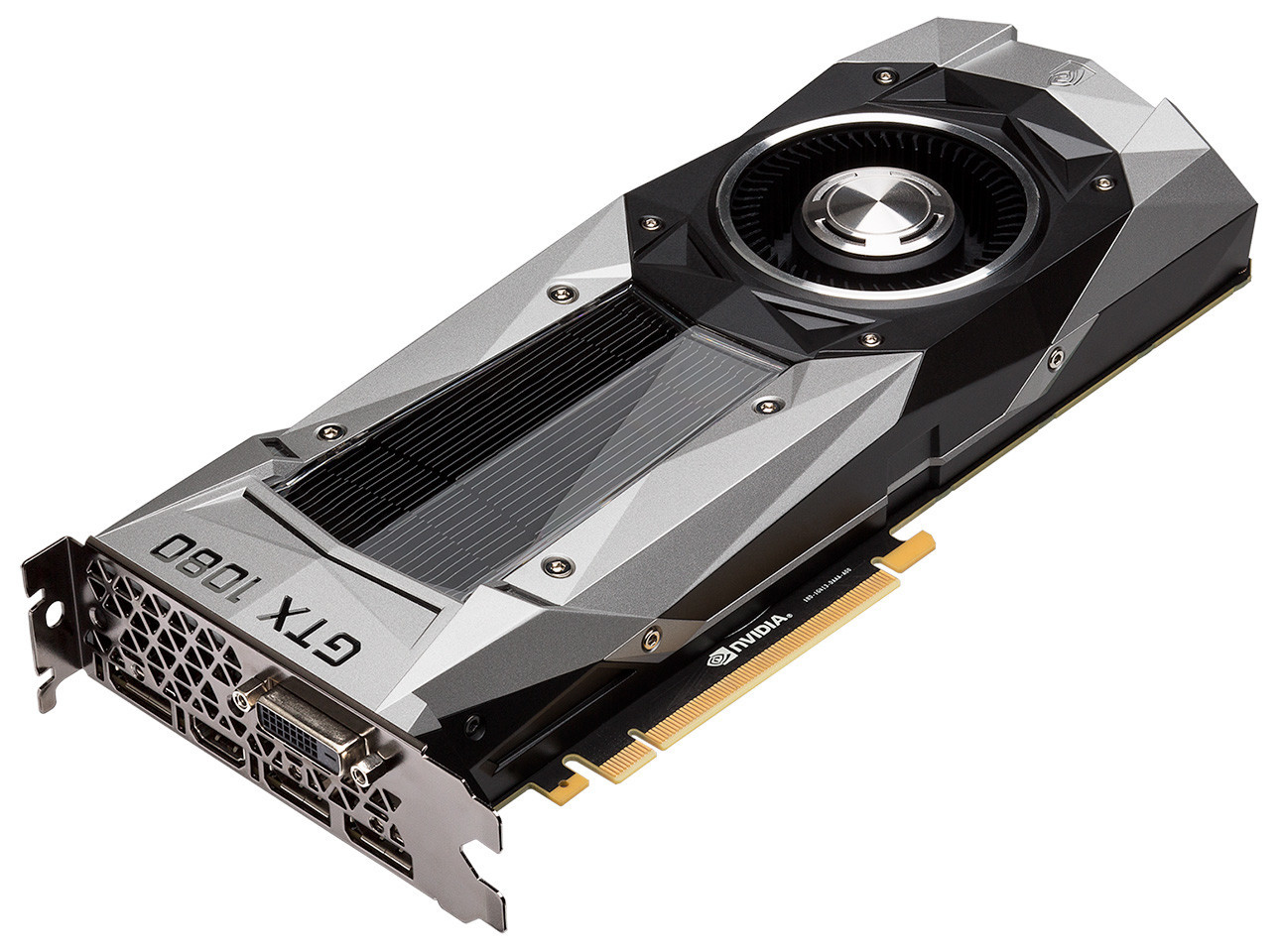
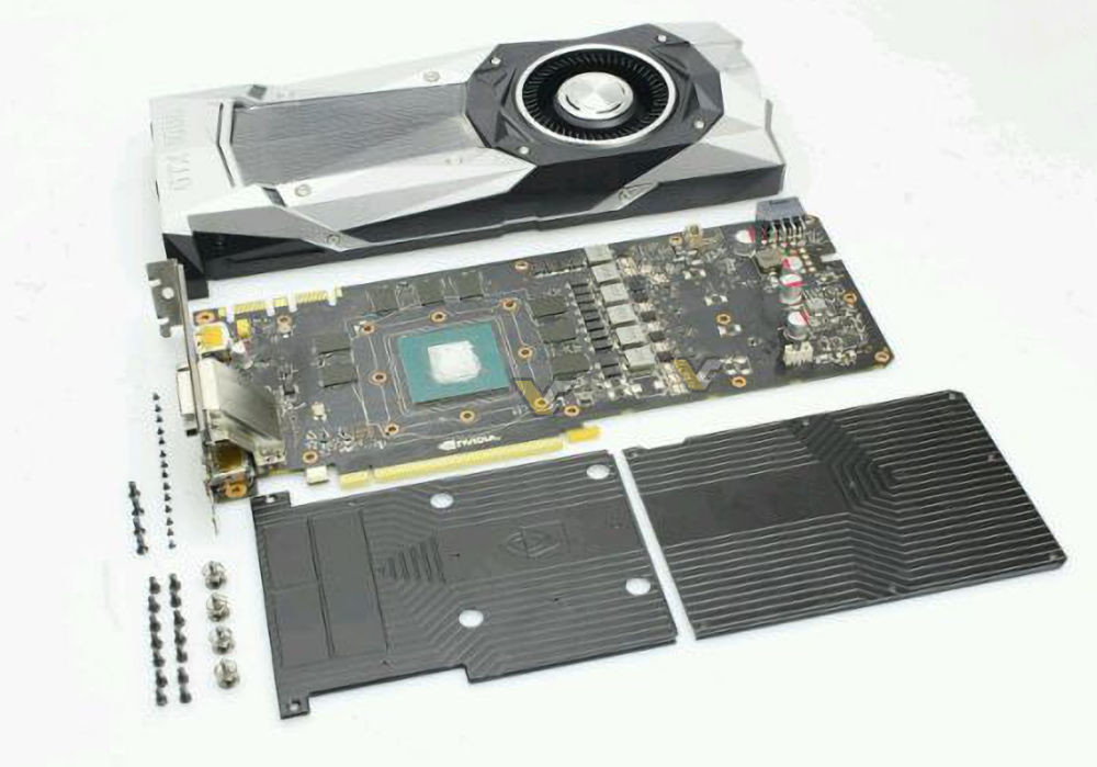
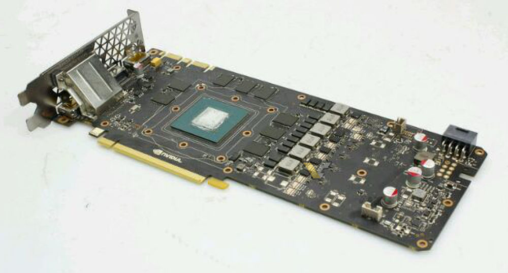
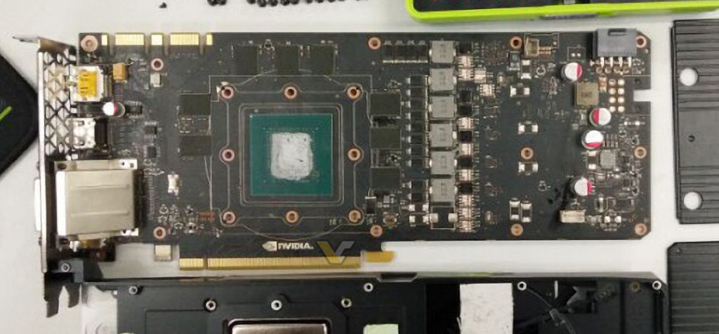
NVIDIA Preparing GeForce GTX 1080 Ti for 2017 CES Launch

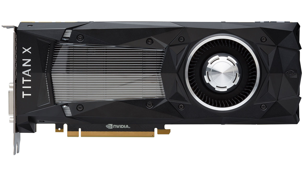
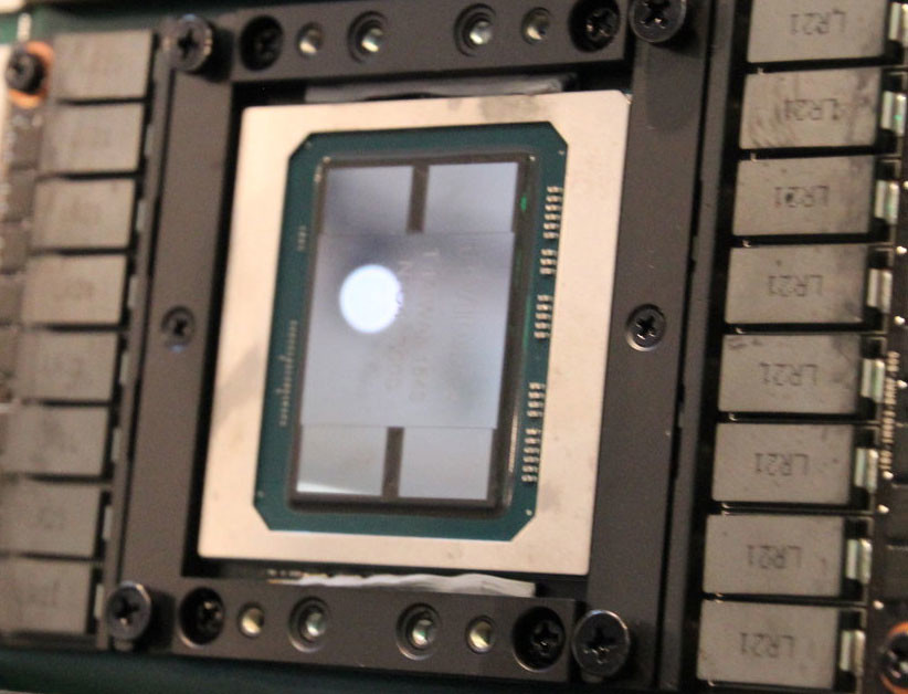
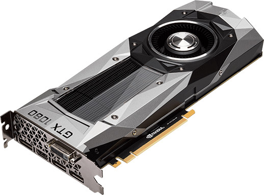
NVIDIA is preparing its next high-end graphics card under the GeForce GTX brand, the GTX 1080 Ti, for launch along the sidelines of the 2017 International CES, early next January. The card will be positioned between the $599-$699 GeForce GTX 1080, and the $1199 TITAN X Pascal, and will be based on the 16 nm "GP102" silicon.

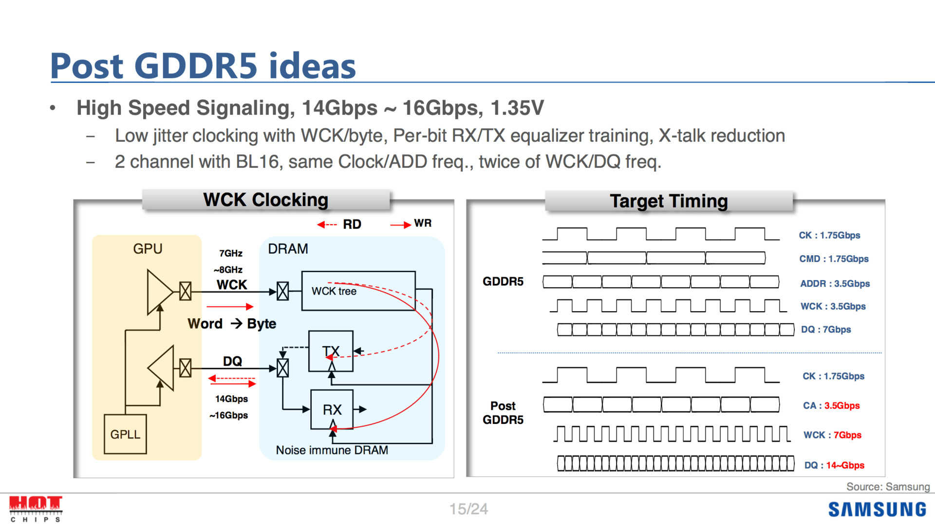
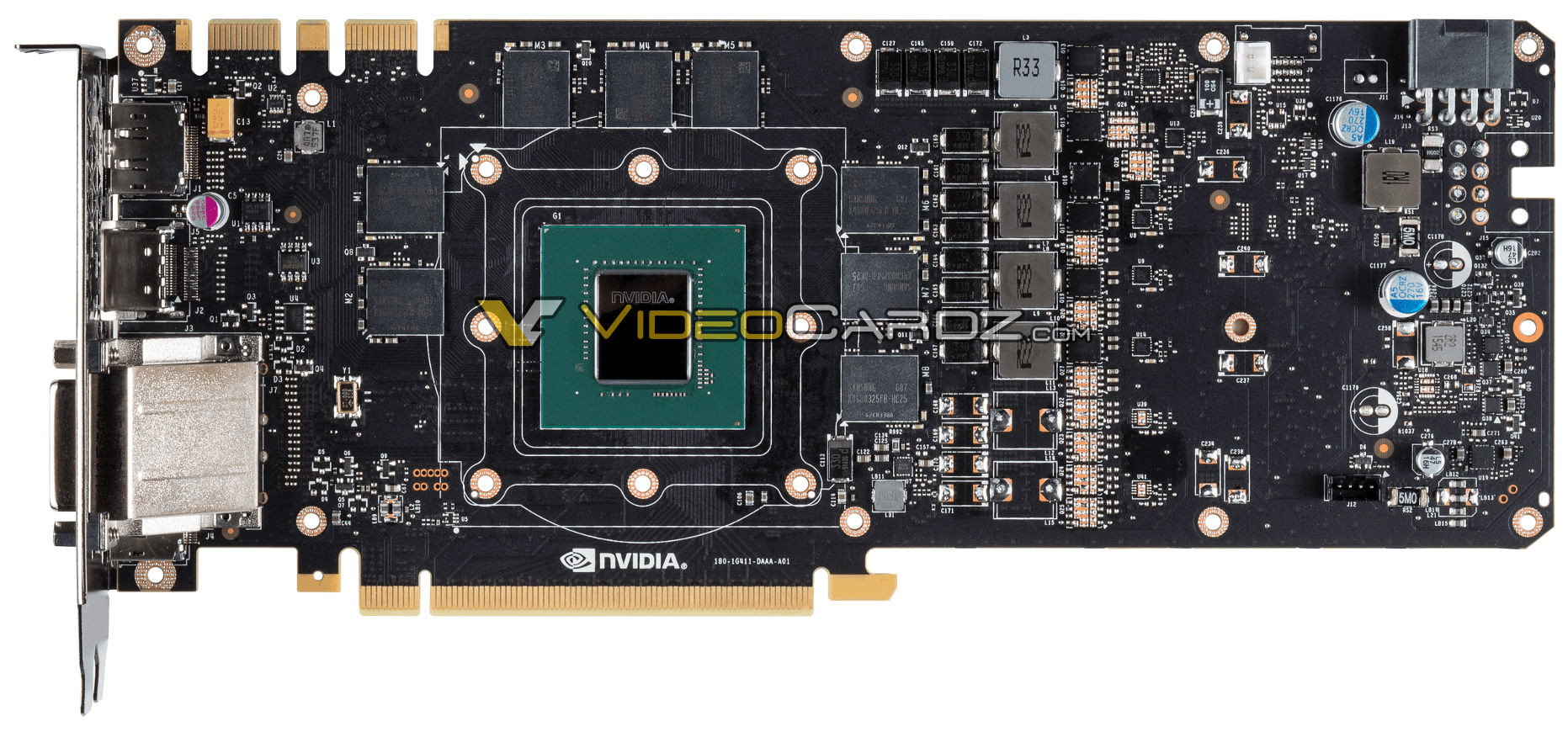
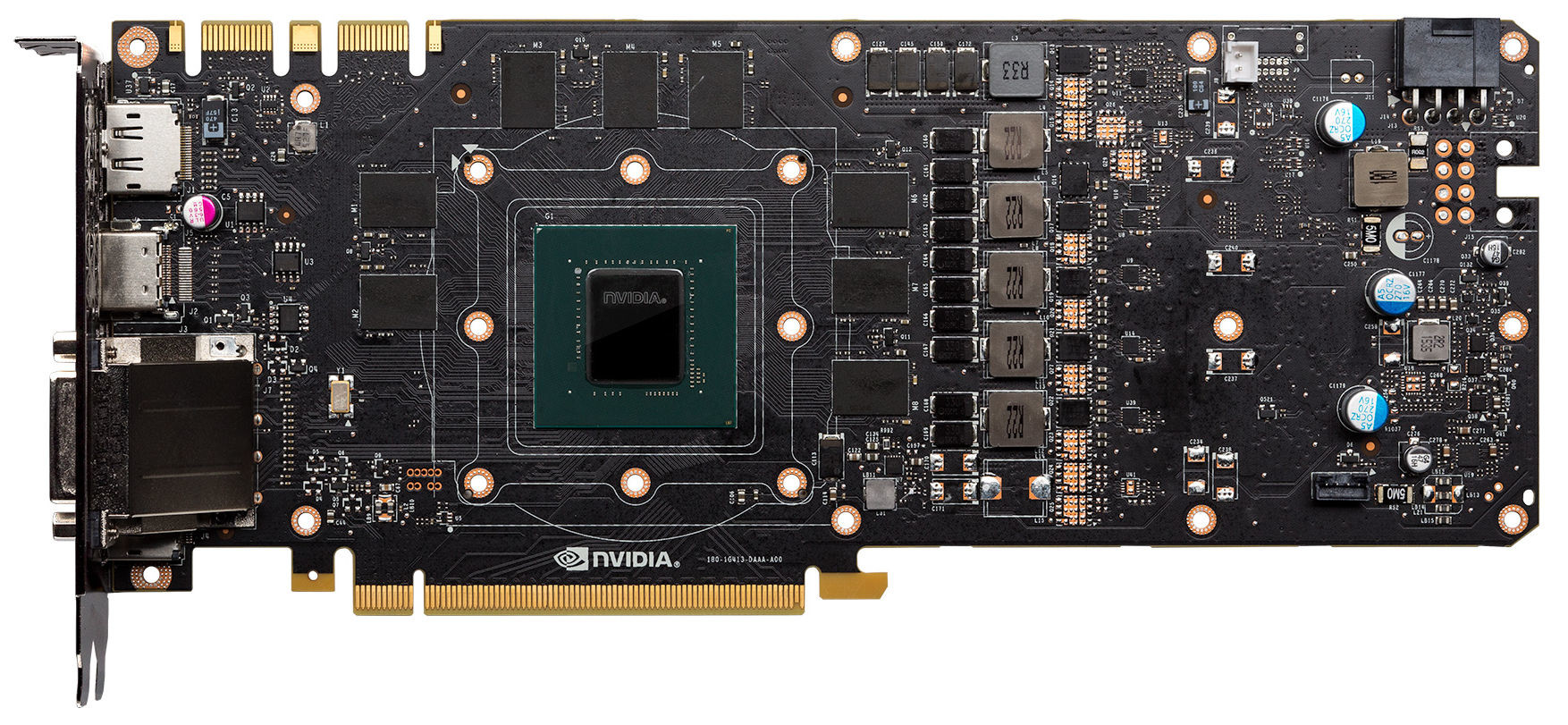
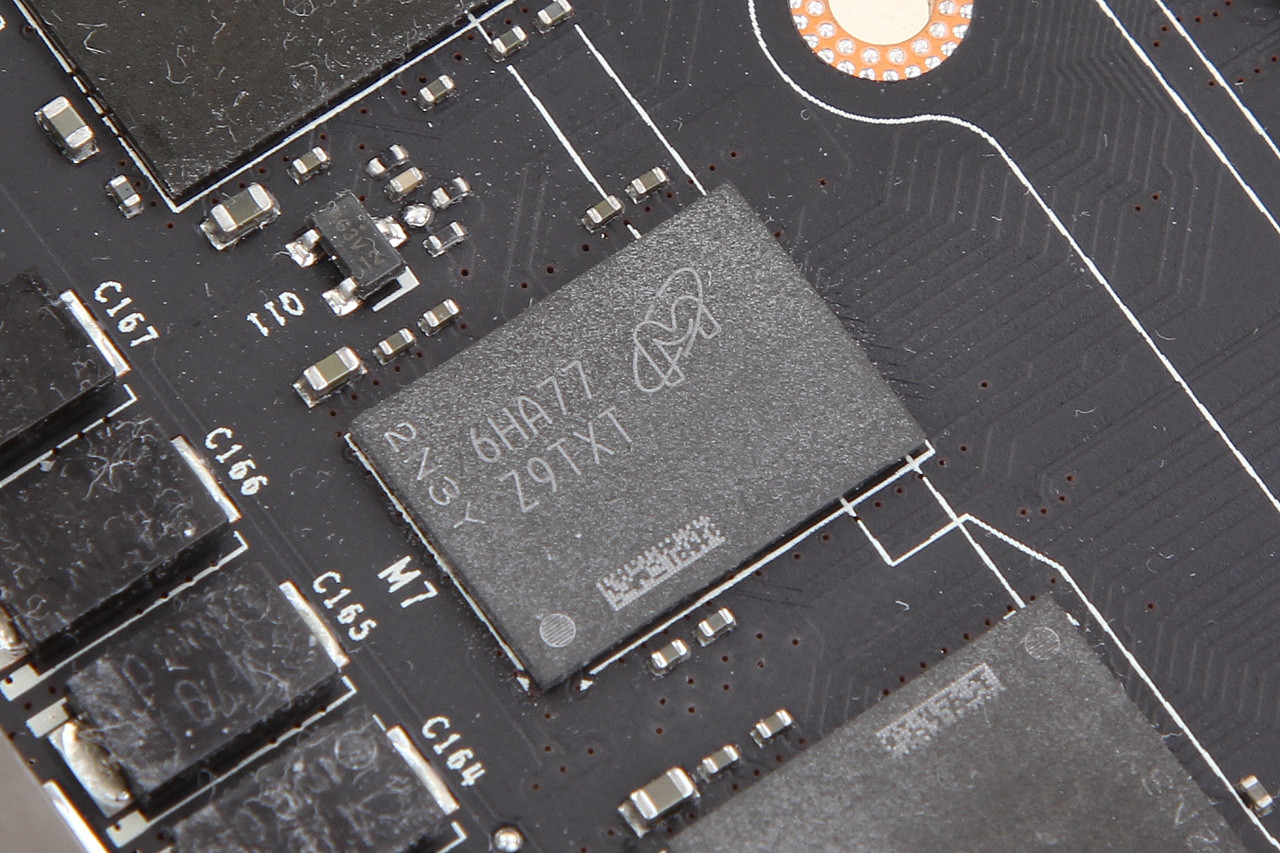
Chinese tech publication Zol.com.cn reports a few possible specifications of the SKU, adding to what we know from an older report. NVIDIA is carving the GTX 1080 Ti out from the GP102 silicon by enabling 26 out of 30 streaming multiprocessors, resulting in a CUDA core count of 3,328. This sets the TMU count at 208. The ROP count is unchanged at 96. The card features a 384-bit wide GDDR5X memory interface (and not the previously-thought GDDR5). It will have an identical memory bandwidth to the TITAN X Pascal, of 480 GB/s. The card will feature 12 GB of standard memory amount. Its GPU clock speeds are expected to be 1503 MHz core, with 1623 MHz GPU Boost.

PNY Announces the GeForce GTX 1080 XLR8 OC Graphics Card

PNY today announced its premium custom-design GeForce GTX 1080 graphics card, the GTX 1080 XLR8 OC. The card combines an NVIDIA reference-design (Founders Edition) PCB with a custom-design air-cooling solution, to support factory-overclocked speeds of 1708 MHz core, 1848 MHz GPU Boost, against reference-design clocks of 1607 MHz core and 1733 MHz GPU Boost. The memory is left untouched at 10 GHz (GDDR5X-effective).

The cooling solution features a split aluminium fin-stack heatsink to which heat drawn directly from the GPU core is fed to two aluminium fin-stacks by 8 mm-thick nickel-plated copper heat pipes. The heatsink is ventilated by a trio of 80 mm fans, which stay off when the GPU is idling. The card draws power from a single 8-pin PCIe power connector, display outputs include three DisplayPort 1.4, and one each of HDMI 2.0b and dual-link DVI. Available now, the PNY GTX 1080 XLR8 OC is priced at US $ 659.99.

Inno3D Announces the GeForce GTX 1080 iChill Black

Inno3D, a leading manufacturer of high-end hardware components and computer utilities, introduces its new flagship Inno3D GeForce GTX 1080 iChiLL BLACK. The iChiLL BLACK edition stands for an industry-leading Hybrid cooling solution that combines super-silent air-flow with ultimate water-cooling. Taking place at the absolute top-of-the-hill, the latest descendant of INNO3D's GeForce GTX 1080 high-end graphics card family, comes with 8GB GDDR5X at a bit-rate of 256bit and a core clock rate at 1759MHz. The DVI, DP and HDMI ports enables the gamer to connect with up to three screens for the ultimate gaming experience.

"We're aiming to satisfy the enthusiast gamer who has ridiculous demands and with our iChiLL BLACK edition they get the Brute among High-End Graphics Cards" states Stanley Wong, Managing Director at INNO3D. "The Hybrid cooling solution makes it possible to squeeze every single drop of performance out of the highest performing components. It not only results in an awesome performing product, it also runs at extremely low noise levels."

EVGA GeForce GTX 1080 HYBRID Launched

EVGA today launched the GeForce GTX 1080 HYBRID graphics card, priced at US $729.99, a $129.99 premium over the GTX 1080 baseline pricing. The card is characterized by a factory-fitted all-in-one, closed-loop liquid cooling solution that works in conjunction with a minor air cooling system. The liquid cooling component cools the factory-overclocked GPU, along with some of the heat from a base-plate cooling the memory and VRM; while a conventional 100 mm fan's air-flow actively cools that base-plate.

The underlying PCB is identical to that of the GTX 1080 Classified ACX 3.0 by EVGA. The card also offers the same factory-overclock as the Classified, with 1721 MHz core, 1860 MHz GPU Boost, and an untouched 10 GHz (GDDR5X-effective) memory. The card draws power from a pair of 8-pin PCIe power connectors, its display outputs include one each of HDMI 2.0b, dual-link DVI, and three DisplayPort 1.4 connectors. EVGA is giving away $115 worth in-game credit with Epic Games' upcoming MOBA title "Paragon" with this card.

Samsung Bets on GDDR6 for 2018 Rollout

Even as its fellow-Korean DRAM maker SK Hynix is pushing for HBM3 to bring 2 TB/s memory bandwidths to graphics cards, Samsung is betting on relatively inexpensive standards that succeed existing ones. The company hopes to have GDDR6, the memory standard that succeeds GDDR5X, to arrive by 2018.

GDDR6 will serve up bandwidths of up to 16 Gbps, up from the 10 Gbps currently offered by GDDR5X. This should enable memory bandwidths of 512 GB/s over a 256-bit wide memory interface, and 768 GB/s over 384-bit. The biggest innovation with GDDR6 that sets it apart from GDDR5X is LP4X, a method with which the memory controller can more responsively keep voltages proportionate to clocks, and reduce power-draw by up to 20% over the previous standard.

NVIDIA Announces the GeForce GTX 10 Series for Notebooks

NVIDIA today announced the GeForce GTX 10-series for notebooks. The lineup includes three SKUs - the GeForce GTX 1080 Mobile, the GTX 1070 Mobile, and the GTX 1060 Mobile. Thanks to huge energy-efficiency gains with the "Pascal" architecture and the new 16 nm silicon fab process, this round of NVIDIA's mobile GPUs aren't "gimped out" in comparison its desktop discrete GPU lineup, in that they SKUs don't feature fewer CUDA cores to their corresponding desktop counterparts.

The lineup begins with the GTX 1080 Mobile. Based on the GP104 silicon, this chip features all 2,560 CUDA cores, 160 TMUs, and 64 ROPs physically present on the chip. The chip is endowed with 8 GB of 256-bit GDDR5X memory ticking at 10 Gbps. The core clock speeds remain unknown. The GTX 1070 Mobile is an interesting SKU in that it is better endowed than its desktop counterpart. It features 2,048 CUDA cores (the desktop GTX 1070 features 1,920), 128 TMUs, 64 ROPs, and 8 GB of 256-bit GDDR5 memory running at 8 Gbps. This chip features 1443 MHz core, and 1645 MHz GPU Boost. At the bottom of the pile is the GTX 1060 Mobile. Based on the GP106 silicon, this chip features 1,280 CUDA cores, 80 TMUs, 48 ROPs, and 6 GB of 192-bit GDDR5 memory running at 8 Gbps; with clock speeds of 1405 MHz core, with 1569 MHz GPU Boost.

CORSAIR Launches Hydro GFX GTX 1080 Liquid Cooled Graphics Card

CORSAIR, a world leader in enthusiast memory, PC components and high-performance gaming hardware today announced the release of its second generation of Hydro GFX Series graphics cards, the CORSAIR Hydro GFX GTX 1080. Harnessing the phenomenal power of an overclocked NVIDIA GeForce GTX 1080 GPU and co-developed in partnership with the expert graphics card team at MSI, the Hydro GFX GTX 1080 completes the package with CORSAIR's industry leading liquid cooling.

The result is a graphics card with the overclocked power to push the limits of 4K and VR gaming performance, while running not just cooler, but also significantly quieter than a stock GeForce GTX 1080. Up to 10% faster and 50% cooler than stock cards, the Hydro GFX GTX 1080 is the GeForce GTX 1080 as it should be.

NVIDIA TITAN X Pascal Available from Today

NVIDIA's flagship graphics card targeted at gamers and PC enthusiasts, the TITAN X Pascal, will be available from today, exclusively through the GeForce website, at this page. NVIDIA will be directly marketing the card. The card is priced at US $1,199 (excl taxes). Based on the 16 nm "GP102," derived from the "Pascal" architecture, the TITAN X Pascal features 3,584 CUDA cores, 224 TMUs, 96 ROPs, and a 384-bit wide GDDR5X memory, holding 12 GB of memory. The chip is clocked at 1417 MHz core, with 1531 MHz GPU Boost, and 10 Gbps memory, working out to 480 GB/s memory bandwidth. Like the GTX 1080 and GTX 1070, the TITAN X Pascal appears to be limited to 2-way SLI.

More pictures follow.

NVIDIA Launches Maxed-out GP102 Based Quadro P6000

Late last week, NVIDIA announced the TITAN X Pascal, its fastest consumer graphics offering targeted at gamers and PC enthusiasts. The reign of TITAN X Pascal being the fastest single-GPU graphics card could be short-lived, as NVIDIA announced a Quadro product based on the same "GP102" silicon, which maxes out its on-die resources. The new Quadro P6000, announced at SIGGRAPH alongside the GP104-based Quadro P5000, features all 3,840 CUDA cores physically present on the chip.

Besides 3,840 CUDA cores, the P6000 features a maximum FP32 (single-precision floating point) performance of up to 12 TFLOP/s. The card also features 24 GB of GDDR5X memory, across the chip's 384-bit wide memory interface. The Quadro P5000, on the other hand, features 2,560 CUDA cores, up to 8.9 TFLOP/s FP32 performance, and 16 GB of GDDR5X memory across a 256-bit wide memory interface. It's interesting to note that neither cards feature full FP64 (double-precision) machinery, and that is cleverly relegated to NVIDIA's HPC product line, the Tesla P-series.

NVIDIA Announces the GeForce GTX TITAN X Pascal

In a show of shock and awe, NVIDIA today announced its flagship graphics card based on the "Pascal" architecture, the GeForce GTX TITAN X Pascal. Market availability of the card is scheduled for August 2, 2016, priced at US $1,199. Based on the 16 nm "GP102" silicon, this graphics card is endowed with 3,584 CUDA cores spread across 56 streaming multiprocessors, 224 TMUs, 96 ROPs, and a 384-bit GDDR5X memory interface, holding 12 GB of memory.

The core is clocked at 1417 MHz, with 1531 MHz GPU Boost, and 10 Gbps memory, churning out 480 GB/s of memory bandwidth. The card draws power from a combination of 6-pin and 8-pin PCIe power connectors, the GPU's TDP is rated at 250W. NVIDIA claims that the GTX TITAN X Pascal is up to 60 percent faster than the GTX TITAN X (Maxwell), and up to 3 times faster than the original GeForce GTX TITAN.

NVIDIA to Unveil GeForce GTX TITAN P at Gamescom

NVIDIA is preparing to launch its flagship graphics card based on the "Pascal" architecture, the so-called GeForce GTX TITAN P, at the 2016 Gamescom, held in Cologne, Germany, between 17-21 August. The card is expected to be based on the GP100 silicon, and could likely come in two variants - 16 GB and 12 GB. The two differ by memory bus width besides memory size. The 16 GB variant could feature four HBM2 stacks over a 4096-bit memory bus; while the 12 GB variant could feature three HBM2 stacks, and a 3072-bit bus. This approach by NVIDIA is identical to the way it carved out Tesla P100-based PCIe accelerators, based on this ASIC. The cards' TDP could be rated between 300-375W, drawing power from two 8-pin PCIe power connectors.

The GP100 and GTX TITAN P isn't the only high-end graphics card lineup targeted at gamers and PC enthusiasts, NVIDIA is also working the GP102 silicon, positioned between the GP104 and the GP100. This chip could lack FP64 CUDA cores found on the GP100 silicon, and feature up to 3,840 CUDA cores of the same kind found on the GP104. The GP102 is also expected to feature simpler 384-bit GDDR5X memory. NVIDIA could base the GTX 1080 Ti on this chip.

MSI Unveils GeForce GTX 1080 and GTX 1070 DUKE Edition Graphics Cards

MSI unveiled a pair of APAC-exclusive DUKE Edition graphics cards, the GeForce GTX 1080 DUKE Edition, and the GeForce GTX 1070 DUKE Edition. The two are characterized by a large triple-fan cooling solution that's optimized for the tropical climate of its target markets; and features a custom-design PCB that appears to be similar in design to the Gaming X series cards.

The cooler is longer than the PCB itself. A back-plate covers the PCB. The cooler features a twin-stack aluminium-fin cooler that's ventilated by three 90 mm fans, an RGB LED-lit "DUKE" logo tops the cooler. The GTX 1080 DUKE Edition, in its "OC Mode" offers clock speeds of 1708 MHz core, 1847 MHz GPU Boost, and 10108 MHz (GDDR5X-effective) memory; while the GTX 1070 DUKE Edition, in its "OC Mode" offers 1607 MHz core, 1797 MHz GPU Boost, and 8108 MHz (GDDR5-effective) memory.

GIGABYTE Unveils the GeForce GTX 1080 Xtreme Gaming Water Cooled

GIGABYTE unveiled a liquid cooled variant of its GeForce GTX 1080 Xtreme Gaming graphics card (model: GV-N1080XTREME W-8GD). The card features the same factory overclocked speeds as the air-cooled GTX 1080 Xtreme Gaming card, but is cooled by the company's latest WaterForce AIO liquid cooling solution. Unlike other AIO liquid cooled custom GTX 1080 cards, this one lacks a liquid-air hybrid setup, and relies entirely on the liquid pump-block to cool not just the GPU, but also the memory and VRM.

The card is plumbed to a 120 mm x 120 mm radiator with a 120 mm spinner. It features RGB LED lighting along the top logo and an "X" shaped ornament over the pump-block. The card features clock speeds of 1784 MHz core, 1936 MHz GPU Boost, and 10.21 GHz (GDDR5X-effective) memory. It features Xtreme VR Link, a secondary display I/O mode that enables three HDMI 2.0b and one dual-link DVI connector in "VR mode," and three DisplayPorts 1.4, one HDMI 2.0b, and one dual-link DVI; in "standard mode." This works through TMDS rerouting, and the additional HDMI ports are put out through internal headers that can either be wired to the rear panel through a bracket, or a front-panel that fits into a 5.25-inch bay. The card is backed by a 4-year warranty.
Many Thanks to newconroer for the tip.

ASUS Announces the GeForce GTX 1080 Turbo

ASUS announced the GeForce GTX 1080 Turbo graphics card (model: TURBO-GTX1080-8G). Positioned below its ROG GTX 1080 STRIX, the card is expected to be priced somewhere between the $599 baseline NVIDIA set for this SKU, and the $679 price at which the company sells the STRIX. Much like the reference-design (Founders Edition) card, the GTX 1080 Turbo features a lateral-flow cooling solution, which pushes hot air out of the case.

The other two things this card has in common with the reference board is clock speeds - 1607 MHz core, 1733 MHz GPU Boost, 10 GHz (GDDR5X-effective) memory; and the need for just a single 8-pin PCIe power connector. The card features an RGB LED lit "ASUS" logo along its top. You also get one 4-pin PWM case-fan header, with which you can drive at least one case fan in sync with the GPU temperatures (the GTX 1080 STRIX features two such headers). The display output layout is similar to the GTX 1080 STRIX, with two each of DisplayPort 1.4 and HDMI 2.0b ports.

NVIDIA GeForce GTX 1070 Reference PCB Pictured

Here's the first picture of an NVIDIA reference-design PCB for the GeForce GTX 1070. The PCB (PG411) is similar to that of the GTX 1080 (PG413), except for two major differences, VRM and memory. The two PCBs are pictured below in that order. The GTX 1070 PCB features one lesser VRM phase compared to the GTX 1080. The other major difference is that it features larger GDDR5 memory chips, compared to the smaller GDDR5X memory chips found on the GTX 1080. These are 8 Gbps chips, and according to an older article, its clock speed is maxed out to specifications, at which the memory bandwidth works out to be 256 GB/s. The GeForce GTX 1070 will be available by 10th June.

NVIDIA GeForce GTX 1080 Ti to be Based on GP102 Silicon

It looks like NVIDIA will have not one, but two "big chips" based on the "Pascal" architecture. The first one of course is the GP100, which made its debut with the Tesla P100 HPC processor. The GP100 is an expensive chip at the outset, featuring a combination of FP32 (single-precision) and FP64 (double-precision) CUDA cores, running up to 3,840 SPFP and 1,920 DPFP, working out to a gargantuan 5,760 CUDA core count. FP64 CUDA cores are practically useless on the consumer-graphics space, particularly in the hands of gamers. The GP100 also features a swanky 4096-bit HBM2 memory interface, with stacked memory dies sitting on the GPU package, making up an expensive multi-chip module. NVIDIA also doesn't want its product development cycle to be held hostage by HBM2 market availability and yields.

NVIDIA hence thinks there's room for a middle-ground between the super-complex GP100, and the rather simple GP104, if a price-war with AMD should make it impossible to sell a GP100-based SKU at $650-ish. Enter the GP102. This ASIC will be targeted at consumer graphics, making up GeForce GTX products, including the GTX 1080 Ti. It is cost-effective, in that it does away with the FP64 CUDA cores found on the GP100, retaining just a 3,840 FP32 CUDA cores count, 33% higher than that of the GP104, just as the GM200 had 33% more CUDA cores than the GM204.

Micron GDDR5X Memory Chip Pictured Up Close

Here are some of the first pictures of a Micron-made GDDR5X memory chip, up close. The picture reveals the 8-gigabit chip's package number "6HA77Z9TXT-2N3Y." The company's part number is "MT58K256M32." The GeForce GTX 1080 is the first production graphics card with GDDR5X memory, and Micron is the first to market with these chips. The GTX 1080 uses eight such 8-gigabit chips across its 256-bit wide memory interface, to make up its 8 GB standard memory amount. The reference-design GTX 1080 features a memory clock speed of 2.50 GHz (actual), or 10 Gbps (effective). The memory bandwidth for the GTX 1080 is a staggering 320 GB/s.

In its company blog post, Micron states: "Designed by our specialized team of Graphics memory engineers in Munich, GDDR5X provides NVIDIA with an unprecedented level of memory bandwidth for their new GeForce GTX 1080. The bandwidth delivered by Micron's GDDR5X memory is the result of thousands of hours of teamwork by some of the most brilliant minds in our two companies." Not only is GDDR5X faster, but also more energy-efficient than the 7 Gbps GDDR5 chips from the previous generation. This particular chip has a module voltage (VDDQ) of 1.35V, its package measures 14 mm x 10 mm x 1.1 mm (LxWxH).

NVIDIA GeForce GTX 1080 Reference PCB Pictured

Here are some of the first pictures of the reference GeForce GTX 1080 PCB. NVIDIA is selling the reference-design card at a $100 premium, branded as "Founders Edition." Pictures reveal the PCB to be less crowded than the GTX 980 reference PCB. The PCB appears to feature a 6-phase VRM with DrMOS chips, drawing power from a single 8-pin PCIe power connector; the 16 nm GP104 ASIC, with a smaller die than the one featured on the 28 nm GM204, neighbored by eight 8 Gbit GDDR5X memory chips, which feature smaller packages than the ones GDDR5 chips usually come in. We wish someone zoomed in on its VRM controller.

NVIDIA GeForce GTX 1080 Specifications Released

After launching its shockingly fast (claimed) GeForce GTX 1080 and GTX 1070 graphics cards, NVIDIA posted specifications of the former. The two are based on NVIDIA's swanky new 16 nm "GP104" silicon, derived from its "Pascal" GPU architecture. The architecture is detailed in our older article, here. The GeForce GTX 1080 leads the pack, featuring four graphics processing clusters, holding 2,560 CUDA cores. The core runs at a scorching 1607 MHz, with a GPU Boost frequency of 1733 MHz. In one of its demos, NVIDIA overclocked this chip to over 2100 MHz, on its reference air cooling, and the GPU barely scraped 67 °C under stress. The GTX 1080 features a 256-bit wide GDDR5X memory interface, holding 8 GB of memory. The memory is clocked at 2500 MHz (10 GHz effective), working out to a memory bandwidth of 320 GB/s.

API support includes DirectX 12 (feature-level 12_1), OpenGL 4.5, and Vulkan. Display outputs include three DisplayPort 1.4 connectors, one HDMI 2.0b, and one dual-link DVI. The reference-design card is 10.5-inch long, and double-slot. It draws power from a single 8-pin PCIe power connector, and its typical board power is rated at 180W. With the GeForce "Pascal" family, instead of caving in to DirectX 12 native multi-GPU, NVIDIA developed its SLI technology further, with the new SLI HB (high-bandwidth) bridge standard. It's essentially a 2-way bridge in which both SLI fingers of the card are used. This doubles bandwidth between the two cards, allowing higher display resolutions, and multi-display setups between high-resolution monitors. The GeForce GTX 1080 will be available from May 27, 2016, starting at US $599. The $379 GTX 1070 specifications will be revealed closer to its June 10, 2016 market availability.

NVIDIA Announces the GeForce GTX 1080, Faster than GTX 980 SLI

NVIDIA announced its next-generation GeForce GTX 1080 graphics card. Based on the "Pascal" architecture, this chip is built on the 16 nm FinFET process. It uses GDDR5X memory at 10 GHz (GDDR5-effective) clock speed. NVIDIA announced major improvements to the VRM that drives graphics cards, that increases switching efficiency. NVIDIA announced that the GeForce GTX 1080 is faster than a GeForce GTX 980 SLI, and a GeForce GTX TITAN X. The air-cooled GTX 1080 runs at a very high clock speed or 2.11 GHz, with 10 GHz memory clocks, at a temperature of 67 degrees C. Available on May 27, it's priced at $599.
More pictures after the break.

AMD Teases Polaris 10 and Polaris 11 ASIC Images

AMD posted a new webpage for its upcoming "Polaris" GPU architecture, outlining its various innovations - 4th gen. Graphics CoreNext, 4K H.265 60 Hz game-streaming, next-generation display engine with support for DisplayPort 1.3 and HDMI 2.0, XConnect Technology, and the foundation of GPUOpen. In this page, the company inadvertently leaked pictures of its upcoming Polaris 10 "Ellesmere" and Polaris 11 "Baffin" ASICs.

The mast image of the page has a faded 3-quarter shot of a "small" GPU with a die that's almost 30% of the package area. This hints at Polaris 11 "Baffin." This chip is rumored to feature a 128-bit GDDR5/GDDR5X memory interface, and so its pin-count, and conversely, package-size is less. Then in its "4th gen GCN" heading image, AMD showed a picture of a bigger GPU. At first glance, you could assume that it's either "Tonga XT" or "Tahiti" looking at its support brace, but VideoCardz observed that the on-package electrical components in this image are arranged nothing like on the "Tonga" or "Tahiti." This could very well be Polaris 10 "Ellesmere."

AMD Polaris 10 "Ellesmere" as Fast as GTX 980 Ti: Rumor

At a presser in Taiwan for its Radeon Pro Duo launch, AMD talked extensively about its upcoming "Polaris" and "Vega" family of GPUs. The company appears to be betting heavily on two SKUs it plans to launch this June, Polaris 10 and Polaris 11. Polaris 10 is an internal designation to Radeon R9 490(X), based on the 14 nm "Ellesmere" silicon. It may be the biggest chip AMD builds on the "Polaris" architecture, but it won't exactly be a "big chip," in that it doesn't succeed "Fiji." That honor is reserved for "Vega," which debuts in early-2017.

The "Ellesmere" silicon is more of AMD's competitor to NVIDIA's GP104. It is rumored that the R9 490(X), based on this silicon, will offer consumers performance rivaling the GeForce GTX 980 Ti (ergo faster than the Radeon R9 Fury X), at a USD $300-ish price point. "Ellesmere" will be a lean-machine, physically featuring up to 2,560 4th generation GCN stream processors (2,304 enabled on Polaris 10), a possible 256-bit GDDR5X memory interface, and a deep sub-200W typical board power rating.

New GP104 ASIC Picture Hints at GTX 1080 with GDDR5X Memory

A new picture of NVIDIA GP104 "Pascal" ASIC surrounded with GDDR5X memory chips hints at the possibility of NVIDIA reserving the new fast memory standard for the GTX 1080, and older GDDR5 for the more affordable GTX 1070. The picture reveals a GP104 chip with the ASIC code "GP104-400-A1," surrounded by eight Micron-made GDDR5X memory chips. We know from an older article that this ASIC code denotes the top-tier GTX 1080. A second picture (recently posted) reveals a "GP104-200-A1" ASIC surrounded by conventional GDDR5 memory chips. This ASIC corresponds to the second-fastest GTX 1070.

GDDR5 and GDDR5X are nearly identical electrically, and it's quite conceivable that the GP104 chip features a memory controller that supports both standards. GDDR5 can be had at speeds of up to 8 Gbps, while GDDR5X chips can range between 10 Gbps thru 12 Gbps initially, with 14 Gbps chips planned for a little later. Besides memory, CUDA core count could be another factor that sets the two SKUs apart. NVIDIA is planning to launch a total of three SKUs based on the GP104 silicon, in June 2016, beginning with the GTX 1080 and GTX 1070 in early-June (probably along the sidelines of Computex 2016), and a third SKU in mid-June.

AMD's GPU Roadmap for 2016-18 Detailed

AMD finalized the GPU architecture roadmap running between 2016 and 2018. The company first detailed this at its Capsaicin Event in mid-March 2016. It sees the company's upcoming "Polaris" architecture, while making major architectural leaps over the current-generation, such as a 2.5-times performance/Watt uplift and driving the company's first 14 nanometer GPUs; being limited in its high-end graphics space presence. Polaris is rumored to drive graphics for Sony's upcoming 4K Ultra HD PlayStation, and as discrete GPUs, it will feature in only two chips - Polaris 10 "Ellesmere" and Polaris 11 "Baffin."

"Polaris" introduces several new features, such as HVEC (h.265) decode and encode hardware-acceleration, new display output standards such as DisplayPort 1.3 and HDMI 2.0; however, since neither Polaris 10 nor Polaris 11 are really "big" enthusiast chips that succeed the current "Fiji" silicon, will likely make do with current GDDR5/GDDR5X memory standards. That's not to say that Polaris 10 won't disrupt current performance-thru-enthusiast lineups, or even have the chops to take on NVIDIA's GP104. First-generation HBM limits the total memory amount to 4 GB over a 4096-bit path. Enthusiasts will have to wait until early-2017 for the introduction of the big-chip that succeeds "Fiji," which will not only leverage HBM2 to serve up vast amounts of super-fast memory; but also feature a slight architectural uplift. 2018 will see the introduction of its successor, codenamed "Navi," which features an even faster memory interface.

AMD to Launch Radeon R7 470 and R9 480 at Computex

Computex 2016 could see some major consumer graphics action, with AMD reportedly planning to launch two mid-thru-performance segment products on the sidelines of the event - the Radeon R7 470, based on the 14 nm "Baffin" (Polaris 11) silicon, and the Radeon R9 480, based on the 14 nm "Ellesmere" (Polaris 10) silicon. The R7 470 could succeed the R7 370 series in not just performance, but also offer a leap in energy efficiency, with a TDP of less than 50W. The R9 480, on the other hand, could feature a TDP of just 110-135W (R9 380 is rated at 190W).

The R9 480, based on the "Ellesmere" (Polaris 10) is shaping up to be a particularly interesting silicon. It's rumored to feature 2,304 stream processors based on the 4th generation Graphics CoreNext architecture, with 2,560 stream processors being physically present on the chip; and a 256-bit wide GDDR5 (GDDR5X-ready) memory controller. 8 GB could be the standard memory amount. AMD could keep the clock speeds relatively low, with 800-1050 MHz GPU clocks. Imagine R9 390-like performance at half its power-draw.
Return to Keyword Browsing
May 29th, 2024 05:15 EDT change timezone

New Forum Posts

Popular Reviews

Controversial News Posts