News Posts matching #HBM2E

Return to Keyword Browsing

Rambus Designs HBM2E Controller and PHY

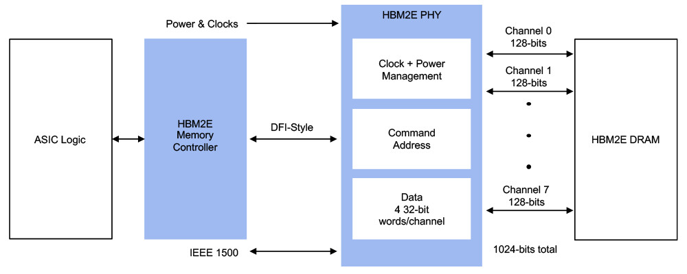
Rambus, a maker of various Interface IP solutions, today announced the latest addition to its high-speed memory interface IP product portfolio in form of High Bandwidth Memory 2E (HBM2E) controller and physical layer (PHY) IP solution. The two IPs are enabling customers to completely integrate the HBM2E memory into their products, given that Rambus provides a complete solution for controlling and interfacing the memory. The design that Ramus offers can support for 12-high DRAM stacks of up to 24 Gb devices, making for up to 36 GB of memory per 3D stack. This single 3D stack is capable of delivering 3.2 Gbps over a 1024-bit wide interface, delivering 410 GB/s of bandwidth per stack.

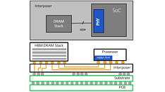
The HBM2E controller core is DFI 3.1 compatible and has support for logic interfaces like AXI, OCP, or a custom one, so the customer can choose a way to integrate this core in their design. With a purchase of their HBM2E IP, Rambus will provide source code written in Hardware Description Language (HDL) and GDSII file containing the layout of the interface.

Samsung Launches 3rd-Generation "Flashbolt" HBM2E Memory

Samsung Electronics, the world leader in advanced memory technology, today announced the market launch of 'Flashbolt', its third-generation High Bandwidth Memory 2E (HBM2E). The new 16-gigabyte (GB) HBM2E is uniquely suited to maximize high performance computing (HPC) systems and help system manufacturers to advance their supercomputers, AI-driven data analytics and state-of-the-art graphics systems in a timely manner.

"With the introduction of the highest performing DRAM available today, we are taking a critical step to enhance our role as the leading innovator in the fast-growing premium memory market," said Cheol Choi, executive vice president of Memory Sales & Marketing at Samsung Electronics. "Samsung will continue to deliver on its commitment to bring truly differentiated solutions as we reinforce our edge in the global memory marketplace."

SK hynix Displays its Semiconductor Technologies Leading the 4th Industrial Revolution

SK hynix Inc. presents its innovative semiconductor technologies leading the 4th Industrial Revolution at CES 2020, the world's largest trade show for IT and consumer electronics in Las Vegas, USA, from January 7-10, 2020. In line with its "Memory Centric World" theme, SK hynix depicts a futuristic city which effectively utilizes enormous amounts of data. The Company also showcases its semiconductor solutions across six crucial business fields - artificial intelligence (AI), augmented reality (AR) / virtual reality (VR), automotive, Internet of Things (IoT), big data and 5G.

Headlining at CES 2020 are SK hynix's memory solutions including HBM2E, DDR5 for servers, and SSD, which are already highly regarded and widely used in 4th industrial fields such as 5G and AI for their stability, speed, power consumption and density excellence. Other cutting-edge products set to make headlines in January are the Company's highly durable LPDDR4X and eMMC 5.1, which are optimized for automobiles. What's more, SK hynix is displaying its LPDDR5 and UFS that enhance the performance of 5G smartphones as well as CIS (CMOS Image Sensor) which is essential in establishing effective environments for AR/VR and IoT.

GLOBALFOUNDRIES and SiFive to Deliver Next Level of High Bandwidth Memory on 12LP

GLOBALFOUNDRIES (GF ) and SiFive, Inc. announced today at GLOBALFOUNDRIES Technology Conference (GTC) in Taiwan that they are working to extend high DRAM performance levels with High Bandwidth Memory (HBM2E) on GF's recently announced 12LP+ FinFET solution, with 2.5D packaging design services to enable fast time-to-market for Artificial Intelligence (AI) applications.

In order to achieve the capacity and bandwidth for data-intensive AI training applications, system designers are challenged with squeezing more bandwidth into a smaller area while maintaining a reasonable power profile. SiFive's customizable high bandwidth memory interface on GF's 12LP platform and 12LP+ solution will enable easy integration of high bandwidth memory into a single System-on-Chip (SoC) solutions to deliver fast, power-efficient data processing for AI applications in the computing and wired infrastructure markets.

SK hynix Inc. Reports Third Quarter 2019 Results

SK hynix Inc. today announced financial results for its third quarter 2019 ended on September 30, 2019. The consolidated third quarter revenue was 6.84 trillion won while the operating profit amounted to 473 billion won and the net income 495 billion won. Operating margin and net margin for the quarter was 7%.

The revenue in the third quarter increased by 6% quarter-over-quarter (QoQ) as demand began to pick up. However, the operating profit fell by 26% QoQ as DRAM unit cost reduction was not enough to offset the price drop. DRAM bit shipments increased by 23% QoQ as the Company actively responded to the new products in the mobile market and purchases from some data center customers also increased. DRAM prices remained weak during the quarter, leading to a 16% drop in the average selling price, with the decline smaller than the previous quarter.

SK Hynix Announces its HBM2E Memory Products, 460 GB/s and 16GB per Stack

SK Hynix Inc. announced today that it has developed HBM2E DRAM product with the industry's highest bandwidth. The new HBM2E boasts approximately 50% higher bandwidth and 100% additional capacity compared to the previous HBM2. SK Hynix's HBM2E supports over 460 GB (Gigabyte) per second bandwidth based on the 3.6 Gbps (gigabits-per-second) speed performance per pin with 1,024 data I/Os (Inputs/Outputs). Through utilization of the TSV (Through Silicon Via) technology, a maximum of eight 16-gigabit chips are vertically stacked, forming a single, dense package of 16 GB data capacity.

SK Hynix's HBM2E is an optimal memory solution for the fourth Industrial Era, supporting high-end GPU, supercomputers, machine learning, and artificial intelligence systems that require the maximum level of memory performance. Unlike commodity DRAM products which take on module package forms and mounted on system boards, HBM chip is interconnected closely to processors such as GPUs and logic chips, distanced only a few µm units apart, which allows even faster data transfer.

Samsung Electronics Introduces New Flashbolt HBM2E High Bandwidth Memory

Samsung Electronics Co., Ltd., the world leader in advanced semiconductor technology, today announced its new High Bandwidth Memory (HBM2E) product at NVIDIA's GPU Technology Conference (GTC) to deliver the highest DRAM performance levels for use in next-generation supercomputers, graphics systems, and artificial intelligence (AI).

The new solution, Flashbolt , is the industry's first HBM2E to deliver a 3.2 gigabits-per-second (Gbps) data transfer speed per pin, which is 33 percent faster than the previous-generation HBM2. Flashbolt has a density of 16Gb per die, double the capacity of the previous generation. With these improvements, a single Samsung HBM2E package will offer a 410 gigabytes-per-second (GBps) data bandwidth and 16 GB of memory.
Return to Keyword Browsing
May 21st, 2024 18:07 EDT change timezone

New Forum Posts

Popular Reviews

Controversial News Posts