News Posts matching #HBM2E

Return to Keyword Browsing

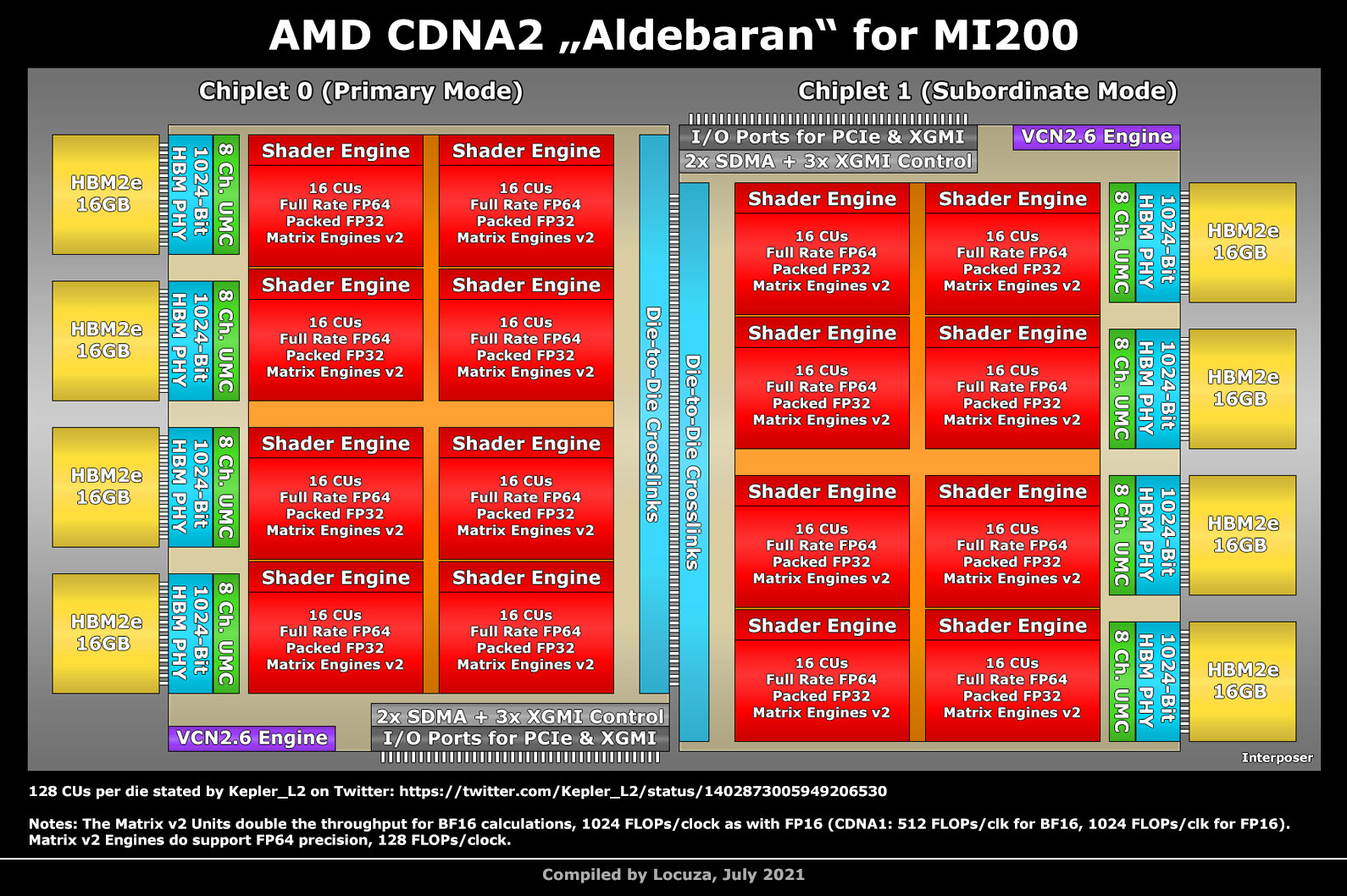
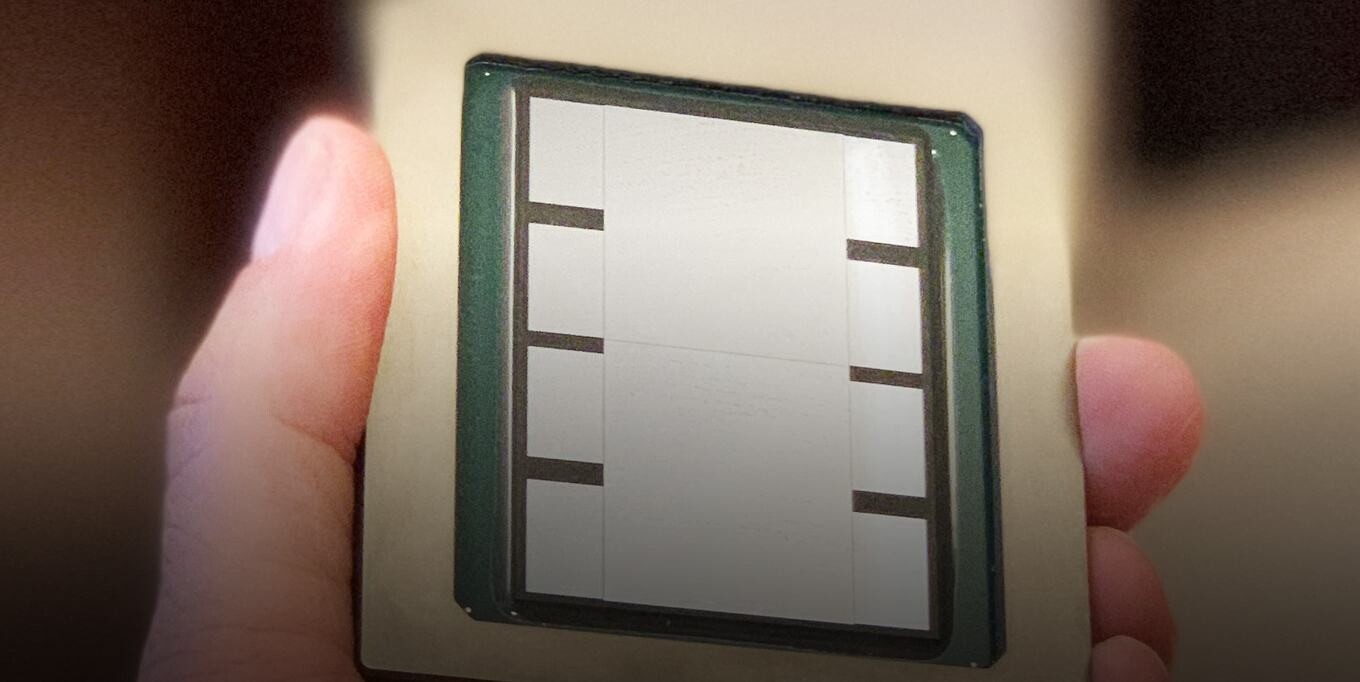
AMD Readies MI250X Compute Accelerator with 110 CUs and 128 GB HBM2E

AMD is preparing an update to its compute accelerator lineup with the new MI250X. Based on the CDNA2 architecture, and built on existing 7 nm node, the MI250X will be accompanied by a more affordable variant, the MI250. According to leaks put out by ExecutableFix, the MI250X packs a whopping 110 compute units (7,040 stream processors), running at 1.70 GHz. The package features 128 GB of HBM2E memory, and a package TDP of 500 W. As for speculative performance numbers, it is expected to offer double-precision (FP64) throughput of 47.9 TFLOP/s, ditto full-precision (FP32), and 383 TFLOP/s half-precision (FP16 and BFLOAT16). AMD's MI200 "Aldebaran" family of compute accelerators are expected to square off against Intel's "Ponte Vecchio" Xe-HPC, and NVIDIA Hopper H100 accelerators in 2022.

Synopsys Accelerates Multi-Die Designs with Industry's First Complete HBM3 IP and Verification Solutions

Synopsys, Inc. today announced the industry's first complete HBM3 IP solution, including controller, PHY, and verification IP for 2.5D multi-die package systems. HBM3 technology helps designers meet essential high-bandwidth and low-power memory requirements for system-on-chip (SoC) designs targeting high-performance computing, AI and graphics applications. Synopsys' DesignWare HBM3 Controller and PHY IP, built on silicon-proven HBM2E IP, leverage Synopsys' interposer expertise to provide a low-risk solution that enables high memory bandwidth at up to 921 GB/s.

The Synopsys verification solution, including Verification IP with built-in coverage and verification plans, off-the-shelf HBM3 memory models for ZeBu emulation, and HAPS prototyping system, accelerates verification from HBM3 IP to SoCs. To accelerate development of HBM3 system designs, Synopsys' 3DIC Compiler multi-die design platform provides a fully integrated architectural exploration, implementation and system-level analysis solution.

NVIDIA Crypto Mining Processor 170HX Card Spotted with 164 MH/s Hash Rate

NVIDIA announced the first four Crypto Mining Processor (CMP) cards earlier this year with performance ranging from 26 MH/s to 86 MH/s. These cards were all based on existing Turing/Ampere silicon and featured board partner-designed cooling systems. NVIDIA appears to have introduced a new flagship model with the passively-cooled 170HX that is based on the NVIDIA A100 accelerator which features a GA100 GPU.

This new model is the first mining card to be designed by NVIDIA and features 4480 CUDA cores paired with 8 GB of HBM2E memory which are both considerably less than what is found in other GA100 based products. NVIDIA has also purposively limited the PCIe interface to Gen 1 x4 to ensure the card cannot be used for tasks outside of cryptocurrency mining. The 170HX has a TDP of 250 W and runs at a base clock of 1140 MHz with a locked-down BIOS that does not allow memory overclocking resulting in a hash rate of 164 MH/s when using the Etash algorithm.

Xilinx Versal HBM Series with Integrated High Bandwidth Memory Tackles Big Data Compute Challenges in the Network and Cloud

Xilinx, Inc., the leader in adaptive computing, today introduced the Versal HBM adaptive compute acceleration platform (ACAP), the newest series in the Versal portfolio. The Versal HBM series enables the convergence of fast memory, secure connectivity, and adaptable compute in a single platform. Versal HBM ACAPs integrate the most advanced HBM2E DRAM, providing 820 GB/s of throughput and 32 GB of capacity for 8X more memory bandwidth and 63% lower power than DDR5 implementations. The Versal HBM series is architected to keep up with the higher memory needs of the most compute intensive, memory bound applications for data center, wired networking, test and measurement, and aerospace and defense.

"Many real-time, high-performance applications are critically bottlenecked by memory bandwidth and operate at the edge of their power and thermal limits," said Sumit Shah, senior director, Product Management and Marketing at Xilinx. "The Versal HBM series eliminates those bottlenecks to provide our customers with a solution that delivers significantly higher performance and reduced system power, latency, form factor, and total cost of ownership for data center and network operators."

AMD MI200 "Aldebaran" Memory Size of 128GB Per Package Confirmed

The 128 GB per package memory size of AMD's upcoming Instinct MI200 HPC accelerator was confirmed, in a document released by Pawsey SuperComputing Centre, a Perth, Australia-based supercomputing firm that's popular with mineral prospecting companies located there. The company is currently working on Setonix, a 50-petaFLOP supercomputer being put together by HP Enterprise, which combines over 750 next-generation "Aldebaran" GPUs (referenced only as "AMD MI-Next GPUs"); and over 200,000 AMD EPYC "Milan" processor cores (the actual processor package count would be lower, and depend on the various core configs the builder is using).

The Pawsey document mentions 128 GB as the per-GPU memory. This corresponds with the rumored per-package memory of "Aldebaran." Recently imagined by Locuza_, an enthusiast who specializes in annotation of logic silicon dies, "Aldebaran" is a multi-chip module of two logic dies and eight HBM2E stacks. Each of the two logic dies, or chiplets, has 8,192 CDNA2 stream processors that add up to 16,384 on the package; and each of the two dies is wired to four HBM2E stacks over a 4096-bit memory bus. These are 128 Gbit (16 GB) stacks, so we have 64 GB memory per logic die, and 128 GB on the package. Find other drool worthy specs of the Pawsey Setonix in the screengrab below.

AMD CDNA2 "Aldebaran" MI200 HPC Accelerator with 256 CU (16,384 cores) Imagined

AMD Instinct MI200 will be an important product for the company in the HPC and AI supercomputing market. It debuts the CDNA2 compute architecture, and is based on a multi-chip module (MCM) codenamed "Aldebaran." PC enthusiast Locuza, who conjures highly detailed architecture based on public information, imagined what "Aldebaran" could look like. The MCM contains two logic dies, and eight HBM2E stacks. Each of the two dies has a 4096-bit HBM2E interface, which talks to 64 GB of memory (128 GB per package). A silicon interposer provides microscopic wiring among the ten dies.

Each of the two logic dies, or chiplets, has sixteen shader engines that have 16 compute units (CU), each. The CDNA2 compute unit is capable of full-rate FP64, packed FP32 math, and Matrix Engines V2 (fixed function hardware for matrix multiplication, accelerating DNN building, training, and AI inference). With 128 CUs per chiplet, assuming the CDNA2 CU has 64 stream processors, one arrives at 8,192 SP. Two such dies add up to a whopping 16,384, more than three times that of the "Navi 21" RDNA2 silicon. Each die further features its independent PCIe interface, and XGMI (AMD's rival to CXL), an interconnect designed for high-density HPC scenarios. A rudimentary VCN (Video CoreNext) component is also present. It's important to note here, that the CDNA2 CU, as well as the "Aldebaran" MCM itself, doesn't have a dual-use as a GPU, since it lacks much of the hardware needed for graphics processing. The MI200 is expected to launch later this year.

NVIDIA Launches A100 PCIe-Based Accelerator with 80 GB HBM2E Memory

During this year's ISC 2021 event, as a part of the company's exhibition portfolio, NVIDIA has decided to launch an updated version of the A100 accelerator. A couple of months ago, in November, NVIDIA launched an 80 GB HBM2E version of the A100 accelerator, on the SXM2 proprietary form-factor. Today, we are getting the same upgraded GPU in the more standard dual-slot PCIe type of card. Featuring a GA100 GPU built on TSMC's 7 nm process, this SKU has 6192 CUDA cores present. To pair with the beefy amount of computing, the GPU needs appropriate memory. This time, there is as much as 80 GB of HBM2E memory. The memory achieves a bandwidth of 2039 GB/s, with memory dies running at an effective speed of 3186 Gbps. An important note is that the TDP of the GPU has been lowered to 250 Watts, compared to the 400 Watt SXM2 solution.

To pair with the new upgrade, NVIDIA made another announcement today and that is an enterprise version of Microsoft's DirectStorage, called NVIDIA GPUDirect Storage. It represents a way of allowing applications to access the massive memory pool built on the GPU, with 80 GB of super-fast HBM2E memory.

NVIDIA and Global Partners Launch New HGX A100 Systems to Accelerate Industrial AI and HPC

NVIDIA today announced it is turbocharging the NVIDIA HGX AI supercomputing platform with new technologies that fuse AI with high performance computing, making supercomputing more useful to a growing number of industries.

To accelerate the new era of industrial AI and HPC, NVIDIA has added three key technologies to its HGX platform: the NVIDIA A100 80 GB PCIe GPU, NVIDIA NDR 400G InfiniBand networking, and NVIDIA Magnum IO GPUDirect Storage software. Together, they provide the extreme performance to enable industrial HPC innovation.

Intel Xeon "Sapphire Rapids" Processor Die Shot Leaks

Thanks to the information coming from Yuuki_Ans, a person which has been leaking information about Intel's upcoming 4th generation Xeon Scalable processors codenamed Sapphire Rapids, we have the first die shots of the Sapphire Rapids processor and its delidded internals to look at. After performing the delidding process and sanding down the metal layers of the dies, the leaker has been able to take a few pictures of the dies present on the processor. As the Sapphire Rapids processor uses multi-chip modules (MCM) approach to building CPUs, the design is supposed to provide better yields for Intel and give the 10 nm dies better usability if defects happen.

In the die shots, we see that there are four dies side by side, with each die featuring 15 cores. That would amount to 60 cores present in the system, however, not all of the 60 cores are enabled. The top SKU is supposed to feature 56 cores, meaning that there would be at least four cores disabled across the configuration. This gives Intel flexibility to deliver plenty of processors, whatever the yields look like. The leaked CPU is an early engineering sample design with a low frequency of 1.3 GHz, which should improve in the final design. Notably, as Sapphire Rapids has SKUs that use in-package HBM2E memory, we don't know if the die configuration will look different from the one pictured down below.

Intel Xe HP "Arctic Sound" 1T and 2T Cards Pictured

Intel has been extensively teasing its Xe HP scalable compute architecture for some time now, and Igor's Lab has an exclusive look at GPU compute cards based on the Xe HP silicon. We know from older reports that Intel's Xe HP compute accelerator packages come in three essential variants—1 tile, 2 tiles, and 4 tiles. A "tile" here is an independent GPU accelerator die. Each of these tiles has 512 execution units, which convert to 4,096 programmable shaders. The single-tile card is a compact, half-height card capable of 1U and 2U chassis. According to Igor's Lab, it comes with 16 GB of HBM2E memory with 716 GB/s memory bandwidth, and the single tile has 384 out of 512 EUs enabled (3,072 shaders). The card also has a typical board power of just 150 W.

The Arctic Sound 2T card is an interesting contraption. A much larger 2-slot card of length easily above 28 cm, and a workstation spacer, the 2T card uses a 2-tile variant of the Xe HP package, but each of the two tiles only has 480 out of 512 EUs enabled. This works out to 7,680 shaders. The dual-chiplet MCM uses 32 GB of HBM2E memory (16 GB per tile), and a typical board power of 300 W. A single 4+4 pin EPS connector, capable of up to 225 W, is used to power the card.

Intel's Upcoming Sapphire Rapids Server Processors to Feature up to 56 Cores with HBM Memory

Intel has just launched its Ice Lake-SP lineup of Xeon Scalable processors, featuring the new Sunny Cove CPU core design. Built on the 10 nm node, these processors represent Intel's first 10 nm shipping product designed for enterprise. However, there is another 10 nm product going to be released for enterprise users. Intel is already preparing the Sapphire Rapids generation of Xeon processors and today we get to see more details about it. Thanks to the anonymous tip that VideoCardz received, we have a bit more details like core count, memory configurations, and connectivity options. And Sapphire Rapids is shaping up to be a very competitive platform. Do note that the slide is a bit older, however, it contains useful information.

The lineup will top at 56 cores with 112 threads, where this processor will carry a TDP of 350 Watts, notably higher than its predecessors. Perhaps one of the most interesting notes from the slide is the department of memory. The new platform will make a debut of DDR5 standard and bring higher capacities with higher speeds. Along with the new protocol, the chiplet design of Sapphire Rapids will bring HBM2E memory to CPUs, with up to 64 GBs of it per socket/processor. The PCIe 5.0 standard will also be present with 80 lanes, accompanying four Intel UPI 2.0 links. Intel is also supposed to extend the x86_64 configuration here with AMX/TMUL extensions for better INT8 and BFloat16 processing.

SiPearl to Manufacture its 72-Core Rhea HPC SoC at TSMC Facilities

SiPearl has this week announced their collaboration with Open-Silicon Research, the India-based entity of OpenFive, to produce the next-generation SoC designed for HPC purposes. SiPearl is a part of the European Processor Initiative (EPI) team and is responsible for designing the SoC itself that is supposed to be a base for the European exascale supercomputer. In the partnership with Open-Silicon Research, SiPearl expects to get a service that will integrate all the IP blocks and help with the tape out of the chip once it is done. There is a deadline set for the year 2023, however, both companies expect the chip to get shipped by Q4 of 2022.

When it comes to details of the SoC, it is called Rhea and it will be a 72-core Arm ISA based processor with Neoverse Zeus cores interconnected by a mesh. There are going to be 68 mesh network L3 cache slices in between all of the cores. All of that will be manufactured using TSMC's 6 nm extreme ultraviolet lithography (EUV) technology for silicon manufacturing. The Rhea SoC design will utilize 2.5D packaging with many IP blocks stitched together and HBM2E memory present on the die. It is unknown exactly what configuration of HBM2E is going to be present. The system will also see support for DDR5 memory and thus enable two-level system memory by combining HBM and DDR. We are excited to see how the final product looks like and now we wait for more updates on the project.

SK hynix Inc. Reports Fiscal Year 2020 and Fourth Quarter Results

SK hynix Inc. today announced financial results for its fiscal year 2020 ended on December 31, 2020. The consolidated revenue of fiscal year 2020 was 31.9 trillion won while the operating profit amounted to 5.013 trillion won, and the net income 4.759 trillion won. Operating margin of for the year was 16%, and net margin was 15%.

"Due to the global pandemic and the intensifying trade disputes last year, the memory market showed sluggish trend," said Kevin (Jongwon) Noh, Executive Vice President and Head of Corporate Center (CFO) at SK hynix. "In the meantime, the Company stably mass-produced its main products such as 1Znm DRAM and 128-layer NAND Flash." Noh also explained, "The Company expanded its server market share based on its quality competitiveness, which resulted in an increase in the revenue and the operating profit by 18% and 84%, respectively, compared to the previous year."

Intel Xe HPC Multi-Chip Module Pictured

Intel SVP for architecture, graphics, and software, Raja Koduri, tweeted the first picture of the Xe HPC scalar compute processor multi-chip module, with its large IHS off. It reveals two large main logic dies built on the 7 nm silicon fabrication process from a third-party foundry. The Xe HPC processor will be targeted at supercomputing and AI-ML applications, so the main logic dies are expected to be large arrays of execution units, spread across what appear to be eight clusters, surrounded by ancillary components such as memory controllers and interconnect PHYs.

There appear to be two kinds of on-package memory on the Xe HPC. The first kind is HBM stacks (from either the HBM2E or HBM3 generation), serving as the main high-speed memory; while the other is a mystery for now. This could either be another class of DRAM, serving a serial processing component on the main logic die; or a non-volatile memory, such as 3D XPoint or NAND flash (likely the former), providing fast persistent storage close to the main logic dies. There appear to be four HBM-class stacks per logic die (so 4096-bit per die and 8192-bit per package), and one die of this secondary memory per logic die.

NVIDIA Announces the A100 80GB GPU for AI Supercomputing

NVIDIA today unveiled the NVIDIA A100 80 GB GPU—the latest innovation powering the NVIDIA HGX AI supercomputing platform—with twice the memory of its predecessor, providing researchers and engineers unprecedented speed and performance to unlock the next wave of AI and scientific breakthroughs. The new A100 with HBM2E technology doubles the A100 40 GB GPU's high-bandwidth memory to 80 GB and delivers over 2 terabytes per second of memory bandwidth. This allows data to be fed quickly to A100, the world's fastest data center GPU, enabling researchers to accelerate their applications even faster and take on even larger models and datasets.

"Achieving state-of-the-art results in HPC and AI research requires building the biggest models, but these demand more memory capacity and bandwidth than ever before," said Bryan Catanzaro, vice president of applied deep learning research at NVIDIA. "The A100 80 GB GPU provides double the memory of its predecessor, which was introduced just six months ago, and breaks the 2 TB per second barrier, enabling researchers to tackle the world's most important scientific and big data challenges."

TSMC to Enter Mass Production of 6th Generation CoWoS Packaging in 2023, up to 12 HBM Stacks

TSMC, the world's leading semiconductor manufacturing company, is rumored to start production of its 6th generation Chip-on-Wafer-on-Substrate (CoWoS) packaging technology. As the silicon scaling is getting ever so challenging, the manufacturers have to come up with a way to get as much performance as possible. That is where TSMC's CoWoS and other chiplet technologies come. They allow designers to integrate many integrated circuits on a single package, making for a cheaper overall product compared to if the product used one big die. So what is so special about 6th generation CoWoS technology from TSMC, you might wonder. The new generation is said to enable a massive 12 stacks of HBM memory on a package. You are reading that right. Imagine if each stack would be an HBM2E variant with 16 GB capacity that would be 192 GB of memory on the package present. Of course, that would be a very expensive chip to manufacture, however, it is just a showcase of what the technology could achieve.

Update 16:44 UTC—TheEnglish DigiTimes report indicates that this technology is expected to see mass production in 2023.

Rambus Advances HBM2E Performance to 4.0 Gbps for AI/ML Training Applications

Rambus Inc. (NASDAQ: RMBS), a premier silicon IP and chip provider making data faster and safer, today announced it has achieved a record 4 Gbps performance with the Rambus HBM2E memory interface solution consisting of a fully-integrated PHY and controller. Paired with the industry's fastest HBM2E DRAM from SK hynix operating at 3.6 Gbps, the solution can deliver 460 GB/s of bandwidth from a single HBM2E device. This performance meets the terabyte-scale bandwidth needs of accelerators targeting the most demanding AI/ML training and high-performance computing (HPC) applications.

"With this achievement by Rambus, designers of AI and HPC systems can now implement systems using the world's fastest HBM2E DRAM running at 3.6 Gbps from SK hynix," said Uksong Kang, vice president of product planning at SK hynix. "In July, we announced full-scale mass-production of HBM2E for state-of-the-art computing applications demanding the highest bandwidth available."

NVIDIA Ampere A100 GPU Gets Benchmark and Takes the Crown of the Fastest GPU in the World

When NVIDIA introduced its Ampere A100 GPU, it was said to be the company's fastest creation yet. However, we didn't know how fast the GPU exactly is. With the whopping 6912 CUDA cores, the GPU can pack all that on a 7 nm die with 54 billion transistors. Paired with 40 GB of super-fast HBM2E memory with a bandwidth of 1555 GB/s, the GPU is set to be a good performer. And how fast it exactly is you might wonder? Well, thanks to the Jules Urbach, the CEO of OTOY, a software developer and maker of OctaneRender software, we have the first benchmark of the Ampere A100 GPU.

Scoring 446 points in OctaneBench, a benchmark for OctaneRender, the Ampere GPU takes the crown of the world's fastest GPU. The GeForce RTX 2080 Ti GPU scores 302 points, which makes the A100 GPU up to 47.7% faster than Turing. However, the fastest Turing card found in the benchmark database is the Quadro RTX 8000, which scored 328 points, showing that Turing is still holding well. The result of Ampere A100 was running with RTX turned off, which could yield additional performance if RTX was turned on and that part of the silicon started working.

SK hynix Starts Mass-Production of HBM2E High-Speed DRAM

SK hynix announced that it has started the full-scale mass-production of high-speed DRAM, 'HBM2E', only ten months after the Company announced the development of the new product in August last year. SK hynix's HBM2E supports over 460 GB (Gigabyte) per second with 1,024 I/Os (Inputs/Outputs) based on the 3.6 Gbps (gigabits-per-second) speed performance per pin. It is the fastest DRAM solution in the industry, being able to transmit 124 FHD (full-HD) movies (3.7 GB each) per second. The density is 16 GB by vertically stacking eight 16 Gb chips through TSV (Through Silicon Via) technology, and it is more than doubled from the previous generation (HBM2).

HBM2E boasts high-speed, high-capacity, and low-power characteristics; it is an optimal memory solution for the next-generation AI (Artificial Intelligence) systems including Deep Learning Accelerator and High-Performance Computing, which all require high-level computing performance. Furthermore, it is expected to be applied to the Exascale supercomputer - a high-performance computing system which can perform calculations a quintillion times per second - that will lead the research of next-generation basic and applied science, such as climate changes, bio-medics, and space exploration.

NVIDIA DGX-A100 Systems Feature AMD EPYC "Rome" Processors

NVIDIA is leveraging the 128-lane PCI-Express gen 4.0 root complex of AMD 2nd generation EPYC "Rome" enterprise processors in building its DGX-A100 super scalar compute systems that leverage the new A100 "Ampere" compute processors. Each DGX-A100 block is endowed with two AMD EPYC 7742 64-core/128-thread processors in a 2P setup totaling 128-cores/256-threads, clocked up to 3.40 GHz boost.

This 2P EPYC "Rome" processor setup is configured to feed PCIe gen 4.0 connectivity to eight NVIDIA A100 GPUs, and 8-port Mellanox ConnectX 200 Gbps InfiniBand NIC. Six NVSwitches provide NVLink connectivity complementing PCI-Express gen 4.0 from the AMD sIODs. The storage and memory subsystem is equally jaw-dropping: 1 TB of hexadeca-channel (16-channel) DDR4 memory, two 1.92 TB NVMe gen 4.0 SSDs, and 15 TB of U.2 NVMe drives (4x 3.84 TB units). The GPU memory of the eight A100 units add up to 320 GB (that's 8x 40 GB, 6144-bit HBM2E). When you power it up, you're greeted with the Ubuntu Linux splash screen. All this can be yours for USD $199,000.

NVIDIA GA100 Scalar Processor Specs Sheet Released

NVIDIA today unveiled the GTC 2020, online event, and the centerpiece of it all is the GA100 scalar processor GPU, which debuts the "Ampere" graphics architecture. Sifting through a mountain of content, we finally found the slide that matters the most - the specifications sheet of GA100. The GA100 is a multi-chip module that has the 7 nm GPU die at the center, and six HBM2E memory stacks at its either side. The GPU die is built on the TSMC N7P 7 nm silicon fabrication process, measures 826 mm², and packing an unfathomable 54 billion transistors - and we're not even counting the transistors on the HBM2E stacks of the interposer.

The GA100 packs 6,912 FP32 CUDA cores, and independent 3,456 FP64 (double-precision) CUDA cores. It has 432 third-generation tensor cores that have FP64 capability. The three are spread across a gargantuan 108 streaming multiprocessors. The GPU has 40 GB of total memory, across a 6144-bit wide HBM2E memory interface, and 1.6 TB/s total memory bandwidth. It has two interconnects: a PCI-Express 4.0 x16 (64 GB/s), and an NVLink interconnect (600 GB/s). Compute throughput values are mind-blowing: 19.5 TFLOPs classic FP32, 9.7 TFLOPs classic FP64, and 19.5 TFLOPs tensor cores; TF32 156 TFLOPs single-precision (312 TFLOPs with neural net sparsity enabled); 312 TFLOPs BFLOAT16 throughout (doubled with sparsity enabled); 312 TFLOPs FP16; 624 TOPs INT8, and 1,248 TOPS INT4. The GPU has a typical power draw of 400 W in the SXM form-factor. We also found the architecture diagram that reveals GA100 to be two almost-independent GPUs placed on a single slab of silicon. We also have our first view of the "Ampere" streaming multiprocessor with its FP32 and FP64 CUDA cores, and 3rd gen tensor cores. The GeForce version of this SM could feature 2nd gen RT cores.

NVIDIA Ampere A100 Has 54 Billion Transistors, World's Largest 7nm Chip

Not long ago, Intel's Raja Koduri claimed that the Xe HP "Ponte Vecchio" silicon was the "big daddy" of Xe GPUs, and the "largest chip co-developed in India," larger than the 35 billion-transistor Xilinix VU19P FPGA co-developed in the country. It turns out that NVIDIA is in the mood for setting records. The "Ampere" A100 silicon has 54 billion transistors crammed into a single 7 nm die (not counting transistor counts of the HBM2E memory stacks).

NVIDIA claims a 20 Times boost in both AI inference and single-precision (FP32) performance over its "Volta" based predecessor, the Tesla V100. The chip also offers a 2.5X gain in FP64 performance over "Volta." NVIDIA has also invented a new number format for AI compute, called TF32 (tensor float 32). TF32 uses 10-bit mantissa of FP16, and the 8-bit exponent of FP32, resulting in a new, efficient format. NVIDIA attributes its 20x performance gains over "Volta" to this. The 3rd generation tensor core introduced with Ampere supports FP64 natively. Another key design focus for NVIDIA is to leverage the "sparsity" phenomenon in neural nets, to reduce their size, and improve performance.

NVIDIA Tesla A100 GPU Pictured

Thanks to the sources of VideoCardz, we now have the first picture of the next-generation NVIDIA Tesla A100 graphics card. Designed for computing oriented applications, the Tesla A100 is a socketed GPU designed for NVIDIA's proprietary SXM socket. In a post few days ago, we were suspecting that you might be able to fit the Tesla A100 GPU in the socket of the previous Volta V100 GPUs as it is a similar SXM socket. However, the mounting holes have been re-arranged and this one requires a new socket/motherboard. The Tesla A100 GPU is based on GA100 GPU die, which we don't know specifications of. From the picture, we can only see that there is one very big die attached to six HBM modules, most likely HBM2E. Besides that everything else is unknown. More details are expected to be announced today at the GTC 2020 digital keynote.
NVIDIA Tesla A100

NVIDIA DGX A100 is its "Ampere" Based Deep-learning Powerhouse

NVIDIA will give its DGX line of pre-built deep-learning research workstations its next major update in the form of the DGX A100. This system will likely pack number of the company's upcoming Tesla A100 scalar compute accelerators based on its next-generation "Ampere" architecture and "GA100" silicon. The A100 came to light though fresh trademark applications by the company. As for specs and numbers, we don't know yet. The "Volta" based DGX-2 has up to sixteen "GV100" based Tesla boards adding up to 81,920 CUDA cores and 512 GB of HBM2 memory. One can expect NVIDIA to beat this count. The leading "Ampere" part could be HPC-focused, featuring a large CUDA-, and tensor core count, besides exotic memory such as HBM2E. We should learn more about it at the upcoming GTC 2020 online event.

SK hynix Inc. Reports First Quarter 2020 Results

SK hynix Inc. today announced financial results for its first quarter 2020 ended on March 31, 2020. The consolidated revenue of first quarter 2020 was 7.20 trillion won while the operating profit amounted to 800 billion won, and the net income 649 billion won. Operating margin for the quarter was 11% and net margin was 9%.

Despite abrupt changes of external business conditions due to COVID-19, our first quarter revenue and operating income increased by 4% and 239% quarter-over-quarter (QoQ) respectively, driven by increased sales of server products, yield rates improvement, and cost reduction. For DRAM, strong demand of server clients offset the weak mobile demand which declined due to both seasonal slowdown and the COVID-19 impact. As a result, the Company's DRAM bit shipments declined only by 4% QoQ and DRAM average selling price increased by 3% QoQ.
Return to Keyword Browsing
May 21st, 2024 19:00 EDT change timezone

New Forum Posts

Popular Reviews

Controversial News Posts