Monday, October 26th 2020

TSMC to Enter Mass Production of 6th Generation CoWoS Packaging in 2023, up to 12 HBM Stacks

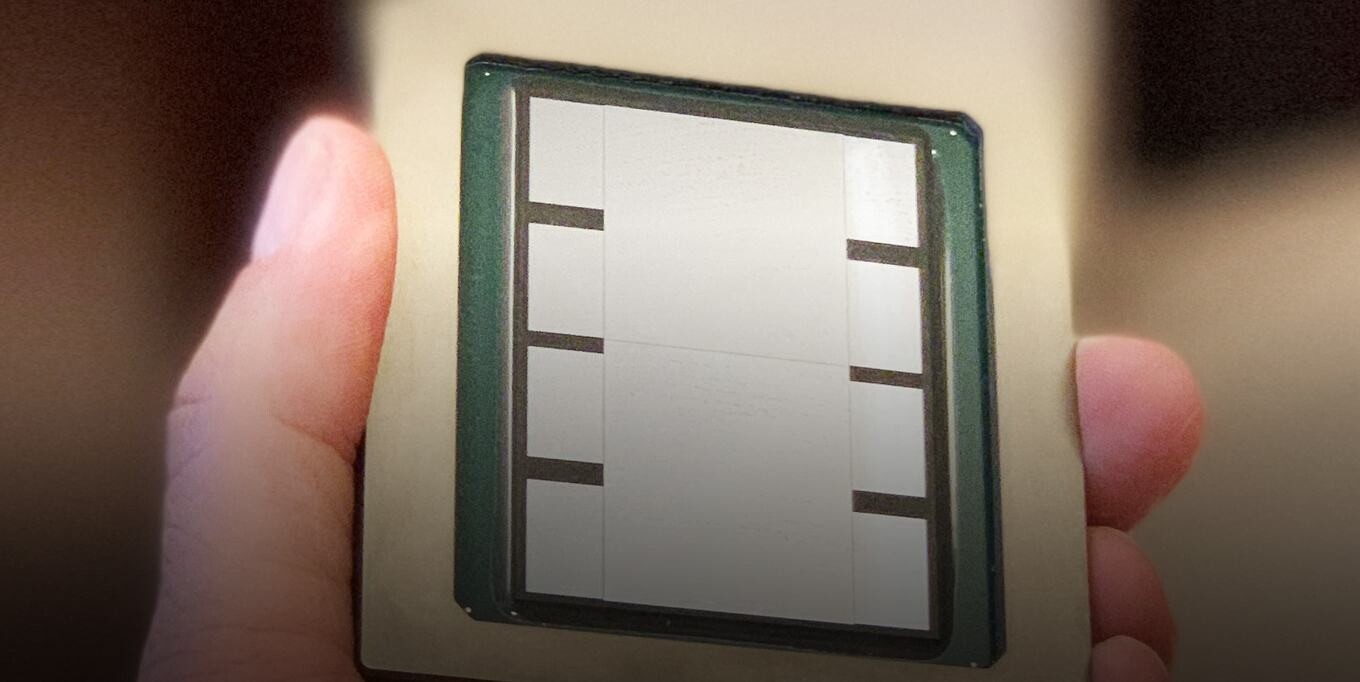
TSMC, the world's leading semiconductor manufacturing company, is rumored to start production of its 6th generation Chip-on-Wafer-on-Substrate (CoWoS) packaging technology. As the silicon scaling is getting ever so challenging, the manufacturers have to come up with a way to get as much performance as possible. That is where TSMC's CoWoS and other chiplet technologies come. They allow designers to integrate many integrated circuits on a single package, making for a cheaper overall product compared to if the product used one big die. So what is so special about 6th generation CoWoS technology from TSMC, you might wonder. The new generation is said to enable a massive 12 stacks of HBM memory on a package. You are reading that right. Imagine if each stack would be an HBM2E variant with 16 GB capacity that would be 192 GB of memory on the package present. Of course, that would be a very expensive chip to manufacture, however, it is just a showcase of what the technology could achieve.

Update 16:44 UTC—TheEnglish DigiTimes report indicates that this technology is expected to see mass production in 2023.
Source: DigiTimes.TW
Add your own comment

12 Comments on TSMC to Enter Mass Production of 6th Generation CoWoS Packaging in 2023, up to 12 HBM Stacks

#1
Sybaris_Caesar
Ian Cutress from Anandtech recently did an interview with Mark Papermaster from AMD. Ian asked Mark about TSMC's CoWoS:
IC: TSMC recently launched its 3D Fabric branding, covering all aspects of its packaging technology. AMD already implements a ‘simple’ CoWoS-S in a number of products, however (there) are other areas such as TSMC’s chip stacking or package-integrated interposers - I assume that AMD looks at these for consideration into the product stack. Can you talk about how AMD approaches the topic, or what’s being considered?
MP:
Our approach to packaging is to partner deeply with the industry - deeply with our foundry partners, deeply with the OSATs. I truly believe that we’re entering a new era of innovation in packaging and interconnect. It’s going to give chip design companies like AMD increasing flexibility going forward. It also creates an environment for increasing collaboration - what you’re seeing is the chiplet technology advance such that you can have more flexibility in co-packaging known good dies. This was always a dream in the industry, and that dream is now becoming reality.
I wonder what's AMD cooking with this.
Posted on Reply
#2
R0H1T
KhonjelIan Cutress from Anandtech recently did an interview with Mark Papermaster from AMD. Ian asked Mark about TSMC's CoWoS:


I wonder what's AMD cooking with this.
A fair one would imagine, aside from the billions Apple spends in getting first dibs at new nodes AMD is by far the most important TSMC customer as far as I'm concerned. Their combined volumes (or wafers?) would likely exceed Apple & even Huawei, especially given what they've lined up for the next several years at TSMC.
Posted on Reply
#3
Valantar
KhonjelIan Cutress from Anandtech recently did an interview with Mark Papermaster from AMD. Ian asked Mark about TSMC's CoWoS:

I wonder what's AMD cooking with this.
There have been rumors of multi-die GPUs being the next step past Navi for quite a few years, so ... RDNA 3? That would certainly be an interesting proposition.
Posted on Reply
#4
delshay
Wow that's impressive, 16GB per stack.
Posted on Reply
#5
Valantar
delshayWow that's impressive, 16GB per stack.
Nothing new about that, HBM2e has been out for a while. Actually the JEDEC standard for that goes up to 24GB per stack, but I don't think anyone has been able to build that yet. (It might also bee that these 12-high stacks are simply too tall to easily implement alongside a die with a high heat output, requiring extremely precisely machined cooling.)
Posted on Reply
#6
Oberon
ValantarThere have been rumors of multi-die GPUs being the next step past Navi for quite a few years, so ... RDNA 3? That would certainly be an interesting proposition.
This and also better integration of chiplets for their CPUs. Plumbing the IF links through the package substrate as they do now is expensive in terms of power and performance. Using CoWoS-l would bring some significant benefits to both. I actually wonder if we'll get to see this with Milan?
Posted on Reply
#7
R0H1T
Using CoWoS would also make it hard to cool, there is a reason why Intel isn't slapping Feveros across the board & a large part of the equation is heat & energy density.
Posted on Reply
#9
Oberon
R0H1TUsing CoWoS would also make it hard to cool, there is a reason why Intel isn't slapping Feveros across the board & a large part of the equation is heat & energy density.
Foveros is a totally different technology. CoWoS (specifically CoWoS-L, which is what is being referred to in this article) is TSMC's version of EMIB.
Posted on Reply
#10
R0H1T
Right, I was thinking PoP or 3D WLP :ohwell:
Posted on Reply
#12
hardcore_gamer
KhonjelIan Cutress from Anandtech recently did an interview with Mark Papermaster from AMD. Ian asked Mark about TSMC's CoWoS:


I wonder what's AMD cooking with this.
My guess is CDNA with HBM.
Posted on Reply
Add your own comment
May 21st, 2024 14:51 EDT change timezone

New Forum Posts

Popular Reviews

Controversial News Posts