News Posts matching #HBM2E

Return to Keyword Browsing

Intel Launches Gaudi 3 AI Accelerator: 70% Faster Training, 50% Faster Inference Compared to NVIDIA H100, Promises Better Efficiency Too

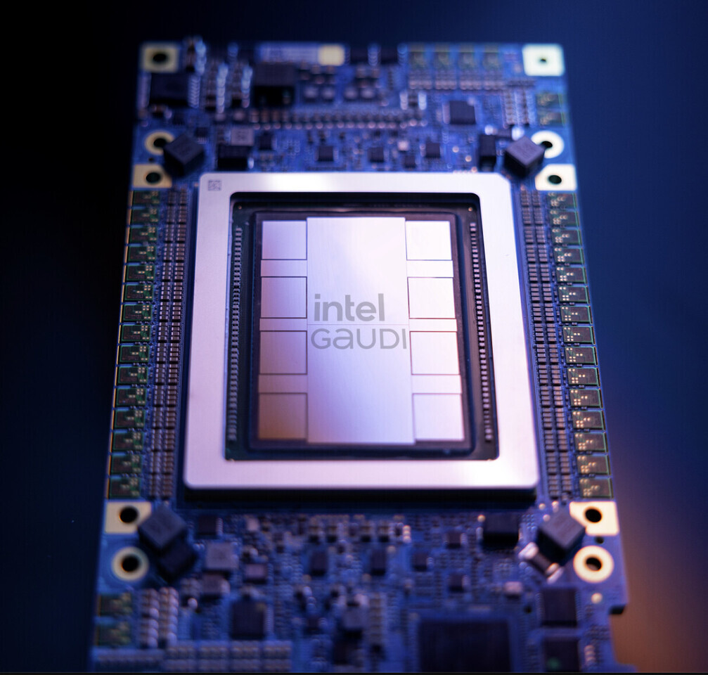
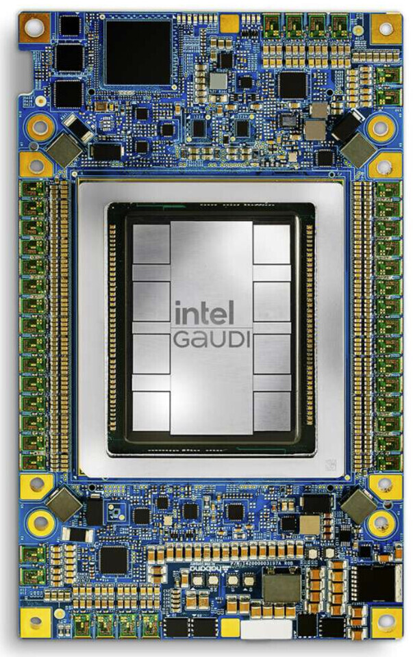
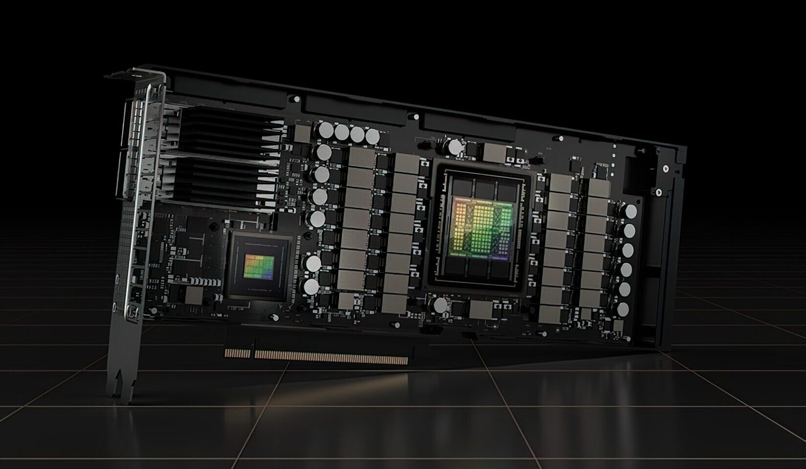
During the Vision 2024 event, Intel announced its latest Gaudi 3 AI accelerator, promising significant improvements over its predecessor. Intel claims the Gaudi 3 offers up to 70% improvement in training performance, 50% better inference, and 40% better efficiency than Nvidia's H100 processors. The new AI accelerator is presented as a PCIe Gen 5 dual-slot add-in card with a 600 W TDP or an OAM module with 900 W. The PCIe card has the same peak 1,835 TeraFLOPS of FP8 performance as the OAM module despite a 300 W lower TDP. The PCIe version works as a group of four per system, while the OAM HL-325L modules can be run in an eight-accelerator configuration per server. This likely will result in a lower sustained performance, given the lower TDP, but it confirms that the same silicon is used, just finetuned with a lower frequency. Built on TSMC's N5 5 nm node, the AI accelerator features 64 Tensor Cores, delivering double the FP8 and quadruple FP16 performance over the previous generation Gaudi 2.

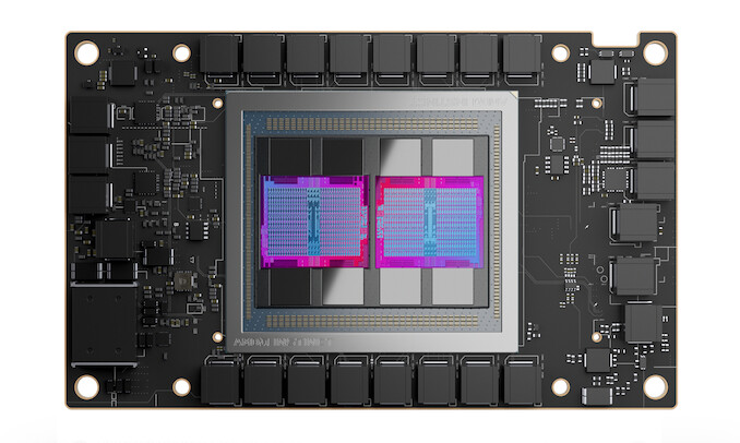
The Gaudi 3 AI chip comes with 128 GB of HBM2E with 3.7 TB/s of bandwidth and 24 200 Gbps Ethernet NICs, with dual 400 Gbps NICs used for scale-out. All of that is laid out on 10 tiles that make up the Gaudi 3 accelerator, which you can see pictured below. There is 96 MB of SRAM split between two compute tiles, which acts as a low-level cache that bridges data communication between Tensor Cores and HBM memory. Intel also announced support for the new performance-boosting standardized MXFP4 data format and is developing an AI NIC ASIC for Ultra Ethernet Consortium-compliant networking. The Gaudi 3 supports clusters of up to 8192 cards, coming from 1024 nodes comprised of systems with eight accelerators. It is on track for volume production in Q3, offering a cost-effective alternative to NVIDIA accelerators with the additional promise of a more open ecosystem. More information and a deeper dive can be found in the Gaudi 3 Whitepaper.

SK Hynix To Invest $1 Billion into Advanced Chip Packaging Facilities

Lee Kang-Wook, Vice President of Research and Development at SK Hynix, has discussed the increased importance of advanced chip packaging with Bloomberg News. In an interview with the media company's business section, Lee referred to a tradition of prioritizing the design and fabrication of chips: "the first 50 years of the semiconductor industry has been about the front-end." He believes that the latter half of production processes will take precedence in the future: "...but the next 50 years is going to be all about the back-end." He outlined a "more than $1 billion" investment into South Korean facilities—his department is hoping to "improve the final steps" of chip manufacturing.

SK Hynix's Head of Packaging Development pioneered a novel method of packaging the third generation of high bandwidth technology (HBM2E)—that innovation secured NVIDIA as a high-profile and long term customer. Demand for Team Green's AI GPUs has boosted the significance of HBM technologies—Micron and Samsung are attempting to play catch up with new designs. South Korea's leading memory supplier is hoping to stay ahead in the next-gen HBM contest—supposedly 12-layer fifth generation samples have been submitted to NVIDIA for approval. SK Hynix's Vice President recently revealed that HBM production volumes for 2024 have sold out—currently company leadership is considering the next steps for market dominance in 2025. The majority of the firm's newly announced $1 billion budget will be spent on the advancement of MR-MUF and TSV technologies, according to their R&D chief.

Intel and Ohio Supercomputer Center Double AI Processing Power with New HPC Cluster

A collaboration including Intel, Dell Technologies, Nvidia and the Ohio Supercomputer Center (OSC), today introduces Cardinal, a cutting-edge high-performance computing (HPC) cluster. Purpose-built to meet the increasing demand for HPC resources in Ohio across research, education and industry innovation, particularly in artificial intelligence (AI).

AI and machine learning are integral tools in scientific, engineering and biomedical fields for solving complex research inquiries. As these technologies continue to demonstrate efficacy, academic domains such as agricultural sciences, architecture and social studies are embracing their potential. Cardinal is equipped with the hardware capable of meeting the demands of expanding AI workloads. In both capabilities and capacity, the new cluster will be a substantial upgrade from the system it will replace, the Owens Cluster launched in 2016.

Manufacturers Anticipate Completion of NVIDIA's HBM3e Verification by 1Q24; HBM4 Expected to Launch in 2026

TrendForce's latest research into the HBM market indicates that NVIDIA plans to diversify its HBM suppliers for more robust and efficient supply chain management. Samsung's HBM3 (24 GB) is anticipated to complete verification with NVIDIA by December this year. The progress of HBM3e, as outlined in the timeline below, shows that Micron provided its 8hi (24 GB) samples to NVIDIA by the end of July, SK hynix in mid-August, and Samsung in early October.

Given the intricacy of the HBM verification process—estimated to take two quarters—TrendForce expects that some manufacturers might learn preliminary HBM3e results by the end of 2023. However, it's generally anticipated that major manufacturers will have definite results by 1Q24. Notably, the outcomes will influence NVIDIA's procurement decisions for 2024, as final evaluations are still underway.

EK Fluid Works Enhances Portfolio with NVIDIA H100 GPU Integration

EK, the leading PC liquid cooling solutions provider, has expanded its hardware support for the EK Fluid Works systems by integrating the state-of-the-art NVIDIA H100 PCIe Tensor Core GPU. NVIDIA's latest release, acclaimed for its unprecedented performance, scalability, and security across diverse workloads, has discovered its ultimate home in EK Fluid Works servers and workstations.

Notably, EK's commitment to sustainability transforms these systems into eco-friendlier platforms, unlocking the full potential of Large Language Models (LLM), machine learning, and AI model training. EK Fluid Works systems emerge as the top choice for those seeking the unleashed power of NVIDIA H100 Tensor Core GPUs, offering an impressive array of efficiency benefits, including:
  • Unparalleled returns on investment
  • The lowest total cost of operation (TCO/OpEx)
  • Minimal additional capital expenditure (CapEx)

BBCube 3D Could be the Future of Stacked DRAM

Scientists at the Tokyo Institute of Technology have developed a new type of stacked or 3D DRAM that the researchers call Bumpless Build Cube 3D or BBCube 3D, which relies on Through Silicon Vias or TSVs to connect the DRAM dies. This is a different approach to HBM which relies on micro bumps to connect the layers together and the Japanese scientists are saying that their bumpless wafer-on-wafer solution should allow not only for an easier manufacturing process, but more importantly, improved cooling, as the TSVs can channel the heat from the DRAM dies down into whatever substrate the BBCube 3D stack is finally mounted onto.

If that wasn't enough, the researchers believe that BBCube 3D will be able to deliver higher speeds than HBM courtesy of a combination of the TSVs being relatively short and "high-density signal parallelism". BBCube 3D is expected to deliver up to a 32 fold increase in bandwidth compared to DDR5 memory and a four fold increase compared to HBM2E memory, while at the same time, drawing less power. The research paper goes into a lot more details for those interested at taking a closer look at this potentially revolutionary shift in DRAM assembly. However, the question that remains unanswered is if this will end up as a real world product some time in the near future, which is all based on how manufacturable BBCube 3D memory will be.

NVIDIA Allegedly Preparing H100 GPU with 94 and 64 GB Memory

NVIDIA's compute and AI-oriented H100 GPU is supposedly getting an upgrade. The H100 GPU is NVIDIA's most powerful offering and comes in a few different flavors: H100 PCIe, H100 SXM, and H100 NVL (a duo of two GPUs). Currently, the H100 GPU comes with 80 GB of HBM2E, both in the PCIe and SXM5 version of the card. A notable exception if the H100 NVL, which comes with 188 GB of HBM3, but that is for two cards, making it 94 GB per each. However, we could see NVIDIA enable 94 and 64 GB options for the H100 accelerator soon, as the latest PCI ID Repository shows.

According to the PCI ID Repository listing, two messages are posted: "Kindly help to add H100 SXM5 64 GB into 2337." and "Kindly help to add H100 SXM5 94 GB into 2339." These two messages indicate that NVIDIA could prepare its H100 in more variations. In September 2022, we saw NVIDIA prepare an H100 variation with 120 GB of memory, but that still isn't official. These PCIe IDs could just come from engineering samples that NVIDIA is testing in the labs, and these cards could never appear on any market. So, we have to wait and see how it plays out.

AMD Confirms that Instinct MI300X GPU Can Consume 750 W

AMD recently revealed its Instinct MI300X GPU at their Data Center and AI Technology Premiere event on Tuesday (June 15). The keynote presentation did not provide any details about the new accelerator model's power consumption, but that did not stop one tipster - Hoang Anh Phu - from obtaining this information from Team Red's post-event footnotes. A comparative observation was made: "MI300X (192 GB HBM3, OAM Module) TBP is 750 W, compared to last gen, MI250X TBP is only 500-560 W." A leaked Giga Computing roadmap from last month anticipated server-grade GPUs hitting the 700 W mark.

NVIDIA's Hopper H100 took the crown - with its demand for a maximum of 700 W - as the most power-hungry data center enterprise GPU until now. The MI300X's OCP Accelerator Module-based design now surpasses Team Green's flagship with a slightly greater rating. AMD's new "leadership generative AI accelerator" sports 304 CDNA 3 compute units, which is a clear upgrade over the MI250X's 220 (CDNA 2) CUs. Engineers have also introduced new 24G B HBM3 stacks, so the MI300X can be specced with 192 GB of memory (as a maximum), the MI250X is limited to a 128 GB memory capacity with its slower HBM2E stacks. We hope to see sample units producing benchmark results very soon, with the MI300X pitted against H100.

Chinese GPU Maker Biren Technology Loses its Co-Founder, Only Months After Revealing New GPUs

Golf Jiao, a co-founder and general manager of Biren Technology, has left the company late last month according to insider sources in China. No official statement has been issued by the executive team at Biren Tech, and Jiao has not provided any details regarding his departure from the fabless semiconductor design company. The Shanghai-based firm is a relatively new startup - it was founded in 2019 by several former NVIDIA, Qualcomm and Alibaba veterans. Biren Tech received $726.6 million in funding for its debut range of general-purpose graphics processing units (GPGPUs), also defined as high-performance computing graphics processing units (HPC GPUs).

The company revealed its ambitions to take on NVIDIA's Ampere A100 and Hopper H100 compute platforms, and last August announced two HPC GPUs in the form of the BR100 and BR104. The specifications and performance charts demonstrated impressive figures, but Biren Tech had to roll back its numbers when it was hit by U.S Government enforced sanctions in October 2022. The fabless company had contracted with TSMC to produce its Biren range, and the new set of rules resulted in shipments from the Taiwanese foundry being halted. Biren Tech cut its work force by a third soon after losing its supply chain with TSMC, and the engineering team had to reassess how the BR100 and BR104 would perform on a process node larger than the original 7 nm design. It was decided that a downgrade in transfer rates would appease the legal teams, and get newly redesigned Biren silicon back onto the assembly line.

Samsung Develops GDDR6W Memory Standard: Double the Bandwidth and Density of GDDR6 Through Packaging Innovations

As advanced graphics and display technologies develop, they are blurring the lines between metaverse and our everyday experience. Much of this important shift is being made possible by the advancement of memory solutions designed for graphics products. One of the biggest challenges for improving virtual reality is taking the complexities of real-world objects and environments and recreating them in a virtual space. Doing so requires massive memory and increased computing power. At the same time, the benefits of creating more true-to-life metaverse will be far reaching, including real-life simulations of complicated scenarios and more, sparking innovation across a number of industries.

This is the central idea behind one of the most popular concepts in virtual reality: digital twin. A digital twin is a virtual representation of an object or space. Updated in real-time in accordance with the actual environment, a digital twin spans the lifecycle of its source and uses simulation, machine learning and reasoning to help decision-making. While until recently this was not feasible proposition due to limitations on data processing and transference, digital twins are now gaining traction thanks to availability of high bandwidth technologies.

NVIDIA Could Launch Hopper H100 PCIe GPU with 120 GB Memory

NVIDIA's high-performance computing hardware stack is now equipped with the top-of-the-line Hopper H100 GPU. It features 16896 or 14592 CUDA cores, developing if it comes in SXM5 of PCIe variant, with the former being more powerful. Both variants come with a 5120-bit interface, with the SXM5 version using HBM3 memory running at 3.0 Gbps speed and the PCIe version using HBM2E memory running at 2.0 Gbps. Both versions use the same capacity capped at 80 GBs. However, that could soon change with the latest rumor suggesting that NVIDIA could be preparing a PCIe version of Hopper H100 GPU with 120 GBs of an unknown type of memory installed.

According to the Chinese website "s-ss.cc" the 120 GB variant of the H100 PCIe card will feature an entire GH100 chip with everything unlocked. As the site suggests, this version will improve memory capacity and performance over the regular H100 PCIe SKU. With HPC workloads increasing in size and complexity, more significant memory allocation is needed for better performance. With the recent advances in Large Language Models (LLMs), AI workloads use trillions of parameters for tranining, most of which is done on GPUs like NVIDIA H100.

Intel Xeon Scalable "Sapphire Rapids" with HBM2E Beaten by Older AMD EPYC "Milan-X" in Leaked Benchmarks

Intel's Xeon Scalable "Sapphire Rapids" processor may have a tough time getting to market, as leaked benchmarks suggest that even its premium HPC models with on-package HBM2E memory are outperformed by AMD's older-generation "Zen 3" EPYC processors. The 64-core/128-thread EPYC "Milan-X" processor based on older "Zen 3" microarchitecture with 3D Vertical Cache (3DV cache) chiplets, allegedly outperforms 52-core/104-thread Xeon Platinum 8472C and 60-core/120-thread Xeon Platinum 8490H "Sapphire Rapids" engineering samples in CPU-Z Bench and V-ray tests that scale across cores. These benchmark scores were compared with those of the EPYC "Milan-X" by Tom's Hardware, in which they well woefully short of the AMD chips.

AMD Releases its CDNA2 MI250X "Aldebaran" HPC GPU Block Diagram

AMD in its HotChips 22 presentation released a block-diagram of its biggest AI-HPC processor, the Instinct MI250X. Based on the CDNA2 compute architecture, at the heart of the MI250X is the "Aldebaran" MCM (multi-chip module). This MCM contains two logic dies (GPU dies), and eight HBM2E stacks, four per GPU die. The two GPU dies are connected by a 400 GB/s Infinity Fabric link. They each have up to 500 GB/s of external Infinity Fabric bandwidth for inter-socket communications; and PCI-Express 4.0 x16 as the host system bus for AIC form-factors. The two GPU dies together make up 58 billion transistors, and are fabricated on the TSMC N6 (6 nm) node.

The component hierarchy of each GPU die sees eight Shader Engines share a last-level L2 cache. The eight Shader Engines total 112 Compute Units, or 14 CU per engine. The CDNA2 compute unit contains 64 stream processors making up the Shader Core, and four Matrix Core Units. These are specialized hardware for matrix/tensor math operations. There are hence 7,168 stream processors per GPU die, and 14,336 per package. AMD claims a 100% increase in double-precision compute performance over CDNA (MI100). AMD attributes this to increases in frequencies, efficient data paths, extensive operand reuse and forwarding; and power-optimization enabling those higher clocks. The MI200 is already powering the Frontier supercomputer, and is working for more design wins in the HPC space. The company also dropped a major hint that the MI300, based on CDNA3, will be an APU. It will incorporate GPU dies, core-logic, and CPU CCDs onto a single package, in what is a rival solution to NVIDIA Grace Hopper Superchip.

BIREN BR100 Detailed: China's AI-HPC Processor Storms into the HPC GPU Big Leagues

If InnoSilicon's Fenghua gaming GPU hit the scene last November seemingly out of nowhere, then another Chinese GPU developer is making waves at HotChips 22, this time in the enterprise space. The BR100 by BIREN is a large AI-HPC GPU-based processor that's China's answer to the Hopper, Ponte Vecchio, and CDNA2, and ensure China's growth as an AI/HPC leader is unaffected in the event of a tech embargo for whatever reason.

The BR100 is an MCM of two planar-silicon dies built on the 7 nm DUV node, with a striking 77 billion transistor-count between them, and 550 W TDP (typical). The chip features 64 GB of on-package HBM2E memory. System bus interfaces include PCI-Express 5.0 x16 with CXL, and eight lanes of a proprietary interconnect called B-Link, which total 2.3 TB/s of bandwidth. The processor supports nearly all popular compute formats except double-precision floating-point, or FP64. Among the supported ones are single-precision or FP32, TF32+, FP16, BF16, INT16, and INT8. BIREN claims up to 256 TFLOP/s FP32, up to 512 TFLOP/s TF32+, up to 1 PFLOP/s BF16, and 2,048 TOPS INT8. This would put it at 2.4 to 2.8 times faster than NVIDIA's "Ampere" A100.

Biren Technology Unveils BR100 7 nm HPC GPU with 77 Billion Transistors

Chinese company Biren Technology has recently unveiled the Biren BR100 HPC GPU during their Biren Explore Summit 2022 event. The Biren BR100 features an in-house chiplet architecture with 77 billion transistors and is manufactured on a 7 nm process using TSMC's 2.5D CoWoS packaging technology. The card is equipped with 300 MB of onboard cache alongside 64 GB of HBM2E memory running at 2.3 TFLOPs. This combination delivers performance above that of the NVIDIA Ampere A100 achieving 1024 TFLOPs in 16-bit floating point operations.

The company also announced the BR104 which features a monolithic design and should offer approximately half the performance of the BR100 at a TDP of 300 W. The Biren BR104 will be available as a standard PCIe card while the BR100 will come in the form of an OAM compatible board with a custom tower cooler. The pricing and availability information for these cards is currently unknown.

BittWare Announces PCIe 5.0/CXL FPGA Accelerators Featuring Intel Agilex M-Series and I-Series to Drive Memory and Interconnectivity Improvements

BittWare, a Molex company, a leading supplier of enterprise-class accelerators for edge and cloud-computing applications, today introduced new card and server-level solutions featuring Intel Agilex FPGAs. The new BittWare IA-860m helps customers alleviate memory-bound application workloads by leveraging up to 32 GB of HBM2E in-package memory and 16-lanes of PCIe 5.0 (with CXL upgrade option). BittWare also added new Intel Agilex I-Series FPGA-based products with the introduction of the IA-440i and IA-640i accelerators, which support high-performance interfaces, including 400G Ethernet and PCIe 5.0 (CXL option). These newest models complement BittWare's existing lineup of Intel Agilex F-Series products to comprise one of the broadest portfolios of Intel Agilex FPGA-based offerings on the market. This announcement reinforces BittWare's commitment to addressing ever-increasing demands of high-performance compute, storage, network and sensor processing applications.

"BittWare is excited to apply Intel's advanced technology to solve increasingly difficult application problems, quickly and at low risk," said Craig Petrie, vice president, Sales and Marketing of BittWare. "Our longstanding collaboration with Intel, expertise with the latest development tools, including OneAPI, as well as alignment with Molex's global supply chain and manufacturing capabilities enable BittWare to reduce development time by 12-to-18 months while ensuring smooth transitions from proof-of-concept to volume product deployment."

Intel Announces "Rialto Bridge" Accelerated AI and HPC Processor

During the International Supercomputing Conference on May 31, 2022, in Hamburg, Germany, Jeff McVeigh, vice president and general manager of the Super Compute Group at Intel Corporation, announced Rialto Bridge, Intel's data center graphics processing unit (GPU). Using the same architecture as the Intel data center GPU Ponte Vecchio and combining enhanced tiles with Intel's next process node, Rialto Bridge will offer up to 160 Xe cores, more FLOPs, more I/O bandwidth and higher TDP limits for significantly increased density, performance and efficiency.

"As we embark on the exascale era and sprint towards zettascale, the technology industry's contribution to global carbon emissions is also growing. It has been estimated that by 2030, between 3% and 7% of global energy production will be consumed by data centers, with computing infrastructure being a top driver of new electricity use," said Jeff McVeigh, vice president and general manager of the Super Compute Group at Intel Corporation.

Intel Meteor Lake, HBM2E-enabled Sapphire Rapids, and Ponte Vecchio Pictured

Intel has allowed the media to get a closer look at the next generation of silicon that will power millions of systems in years to come during its private Vision event. PC Watch, a Japanese tech media, managed to get some shots of the upcoming Meteor Lake, Sapphire Rapids, and Ponte Vecchio processors. Starting with Meteor Lake, Intel has displayed two packages for this processor family. The first one is the ultra-compact, high-density UP9 package used for highly compact mobile systems, and it is made out of silicon with minimal packaging to save space. The second one is a traditional design with more oversized packaging, designed for typical laptop/notebook configurations.

Intel Details Ponte Vecchio Accelerator: 63 Tiles, 600 Watt TDP, and Lots of Bandwidth

During the International Solid-State Circuits Conference (ISSCC) 2022, Intel gave us a more significant look at its upcoming Ponte Vecchio HPC accelerator and how it operates. So far, Intel convinced us that the company created Ponte Vecchio out of 47 tiles glued together in one package. However, the ISSCC presentation shows that the accelerator is structured rather interestingly. There are 63 tiles in total, where 16 are reserved for compute, eight are used for RAMBO cache, two are Foveros base tiles, two represent Xe-Link tiles, eight are HBM2E tiles, and EMIB connection takes up 11 tiles. This totals for about 47 tiles. However, an additional 16 thermal tiles used in Ponte Vecchio regulate the massive TDP output of this accelerator.

What is interesting is that Intel gave away details of the RAMBO cache. This novel SRAM technology uses four banks of 3.75 MB groups total of 15 MB per tile. They are connected to the fabric at 1.3 TB/s connection per chip. In contrast, compute tiles are connected at 2.6 TB/s speeds to the chip fabric. With eight RAMBO cache tiles, we get an additional 120 MB SRAM present. The base tile is a 646 mm² die manufactured in Intel 7 semiconductor process and contains 17 layers. It includes a memory controller, the Fully Integrated Voltage Regulators (FIVR), power management, 16-lane PCIe 5.0 connection, and CXL interface. The entire area of Ponte Vecchio is rather impressive, as 47 active tiles take up 2,330 mm², whereas when we include thermal dies, the total area jumps to 3,100 mm². And, of course, the entire package is much larger at 4,844 mm², connected to the system with 4,468 pins.

NVIDIA CMP 170HX Mining Card Tested, Based on GA100 GPU SKU

NVIDIA's Crypto Mining (CMP) series of graphics cards are made to work only for one purpose: mining cryptocurrency coins. Hence, their functionality is somewhat limited, and they can not be used for gaming as regular GPUs can. Today, Linus Tech Tips got ahold of NVIDIA's CMP 170HX mining card, which is not listed on the company website. According to the source, the card runs on NVIDIA's GA100-105F GPU, a version based on the regular GA100 SXM design used in data-center applications. Unlike its bigger brother, the GA100-105F SKU is a cut-down design with 4480 CUDA cores and 8 GB of HBM2E memory. The complete design has 6912 cores and 40/80 GB HBM2E memory configurations.

As far as the reason for choosing 8 GB HBM2E memory goes, we know that the Ethereum DAG file is under 5 GB, so the 8 GB memory buffer is sufficient for mining any coin out there. It is powered by an 8-pin CPU power connector and draws about 250 Watts of power. It can be adjusted to 200 Watts while retaining the 165 MH/s hash rate for Ethereum. This reference design is manufactured by NVIDIA and has no active cooling, as it is meant to be cooled in high-density server racks. Only a colossal heatsink is attached, meaning that the cooling needs to come from a third party. As far as pricing is concerned, Linus managed to get this card for $5000, making it a costly mining option.
More images follow...

Samsung Electronics Expands its "Green Chip" Line-Up

Samsung Electronics Co., Ltd., a world leader in advanced semiconductor technology, today announced that five of its memory products achieved global recognition for successfully reducing its carbon emission, while 20 additional memory products received carbon footprint certification. Samsung's automotive LED packages also had their carbon footprint verification, a first in the industry for automotive LED packages, further expanding Samsung's portfolio of eco-conscious "green chips".

"It is exciting to see our environmentally sustainable efforts receiving global acknowledgements," said Seong-dai Jang, Senior Vice President and Head of DS Corporate Sustainability Management Office at Samsung Electronics. "We will continue our path towards a sustainable future with 'greener' chips enabled by Samsung's cutting-edge technology."

Intel's Sapphire Rapids Xeons to Feature up to 64 GB of HBM2e Memory

During the Supercomputing (SC) 21 event, Intel has disclosed additional information regarding the company's upcoming Xeon server processor lineup, codenamed Sapphire Rapids. One of the central areas of improvement for the new processor generation is the core architecture based on Golden Cove, the same core found in Alder Lake processors for consumers. However, the only difference between the Golden Cove variant found in Alder Lake and Sapphire Rapids is the amount of L2 (level two) cache. With Alder Lake, Intel equipped each core with 1.25 MB of its L2 cache. However, with Sapphire Rapids, each core receives a 2 MB bank.

One of the most exciting things about the processors, confirmed by Intel today, is the inclusion of High-Bandwidth Memory (HBM). These processors operate with eight memory channels carrying DDR5 memory and offer PCIe Gen5 IO expansion. Intel has confirmed that Sapphire Rapids Xeons will feature up to 64 GB of HBM2E memory, including a few operating modes. The first is a simple HBM caching mode, where the HBM memory acts as a buffer for the installed DDR5. This method is transparent to software and allows easy usage. The second method is Flat Mode, which means that both DDR5 and HBM are used as contiguous address spaces. And finally, there exists an HBM-only mode that utilizes the HBM2E modules as the only system memory, and applications fit inside it. This has numerous benefits, primarily drawn from HBM's performance and reduced latency.

SK hynix Receives ISO 26262 FSM Certification

SK hynix announced that it has received an ISO 26262: 2018 FSM (Functional Safety Management) certification, the international standard for functional safety in automotive semiconductors. The global automotive functional safety certification institute, TUV Nord, conducted the assessment. Both companies commemorated the distinction by hosting an online ceremony. In attendance at the ceremony were Daeyong Shim, Head of Automotive Business, and Junho Song, Head of Quality System, from SK hynix and Bianca Pfuff, Profit Center Manager Functional Safety and Deputy Head of Certification Body SEECERT, and Josef Neumann, Senior Project Manager Functional Safety, from TUV Nord.

The ISO 26262 is the international standard for automobile functional safety established by the International Organization for Standardization (ISO) in 2011 to prevent accidents caused by automotive electrical and electronic systems failures. This certification awarded to SK hynix, ISO 26262: 2018, is the latest version with additional requirements for automotive semiconductors. In the automotive industry, safety, quality, and reliability are paramount. Therefore, it is becoming essential that producers of car electronic device related to safety meet ISO 26262 standards.

AMD Instinct MI200: Dual-GPU Chiplet; CDNA2 Architecture; 128 GB HBM2E

AMD today announced the debut of its 6 nm CDNA2 (Compute-DNA) architecture in the form of the MI200 family. The new, dual-GPU chiplet accelerator aims to lead AMD into a new era of High Performance Computing (HPC) applications, the high margin territory it needs to compete in for continued, sustainable growth. To that end, AMD has further improved on a matured, compute-oriented architecture born with Graphics Core Next (GCN) - and managed to improve performance while reducing total die size compared to its MI100 family.

AMD Readies MI250X Compute Accelerator with 110 CUs and 128 GB HBM2E

AMD is preparing an update to its compute accelerator lineup with the new MI250X. Based on the CDNA2 architecture, and built on existing 7 nm node, the MI250X will be accompanied by a more affordable variant, the MI250. According to leaks put out by ExecutableFix, the MI250X packs a whopping 110 compute units (7,040 stream processors), running at 1.70 GHz. The package features 128 GB of HBM2E memory, and a package TDP of 500 W. As for speculative performance numbers, it is expected to offer double-precision (FP64) throughput of 47.9 TFLOP/s, ditto full-precision (FP32), and 383 TFLOP/s half-precision (FP16 and BFLOAT16). AMD's MI200 "Aldebaran" family of compute accelerators are expected to square off against Intel's "Ponte Vecchio" Xe-HPC, and NVIDIA Hopper H100 accelerators in 2022.
Return to Keyword Browsing
May 1st, 2024 02:00 EDT change timezone

New Forum Posts

Popular Reviews

Controversial News Posts