Monday, November 8th 2021

AMD Instinct MI200: Dual-GPU Chiplet; CDNA2 Architecture; 128 GB HBM2E
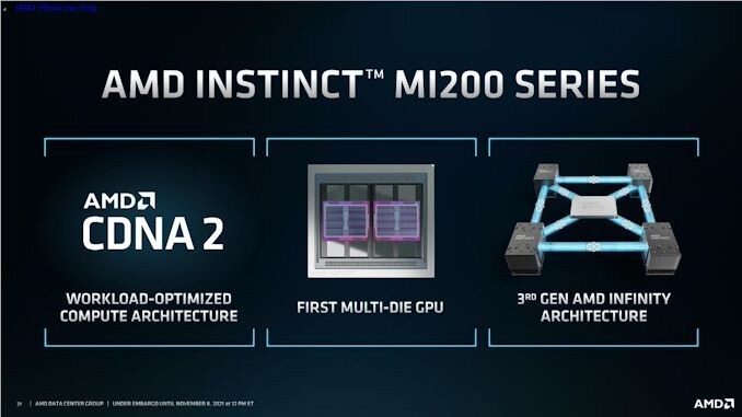
AMD today announced the debut of its 6 nm CDNA2 (Compute-DNA) architecture in the form of the MI200 family. The new, dual-GPU chiplet accelerator aims to lead AMD into a new era of High Performance Computing (HPC) applications, the high margin territory it needs to compete in for continued, sustainable growth. To that end, AMD has further improved on a matured, compute-oriented architecture born with Graphics Core Next (GCN) - and managed to improve performance while reducing total die size compared to its MI100 family.


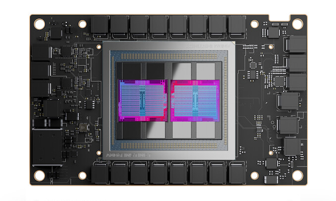
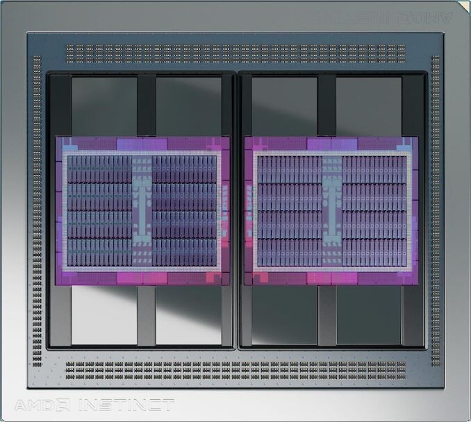
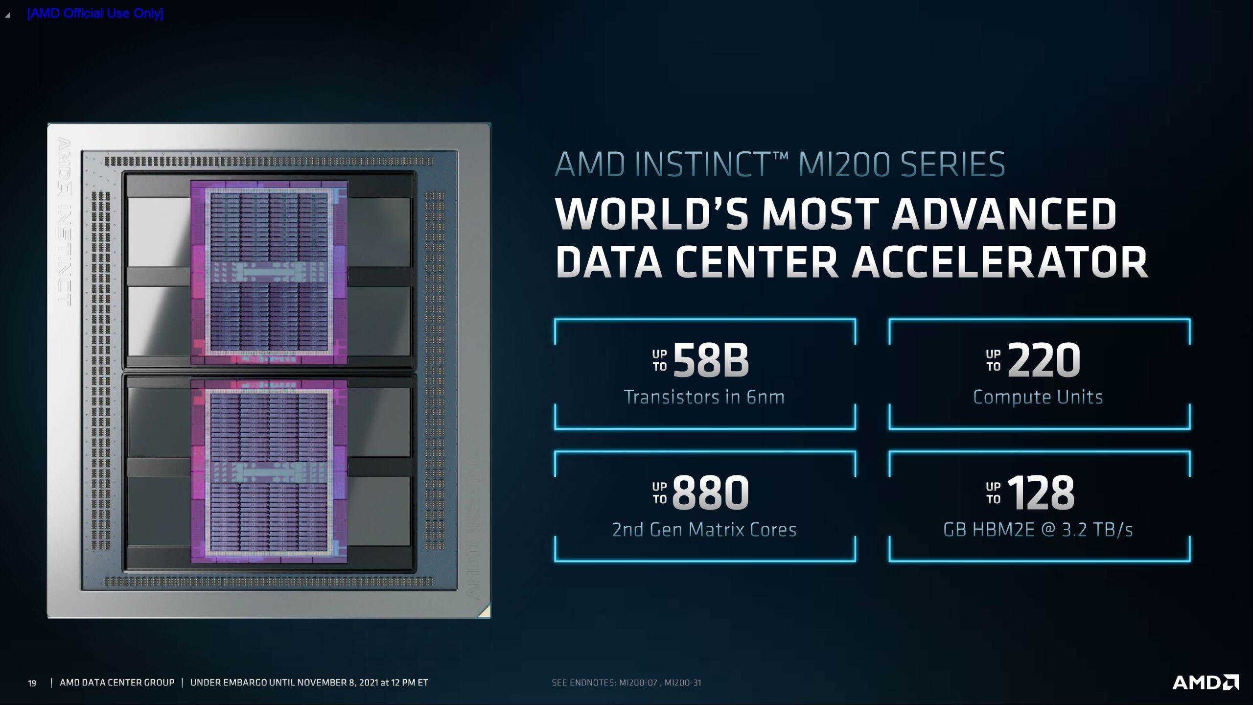
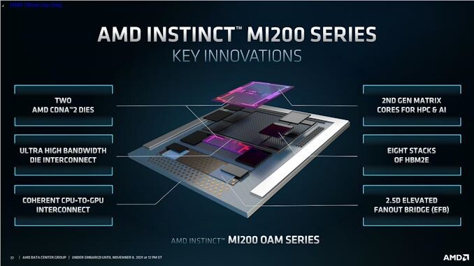
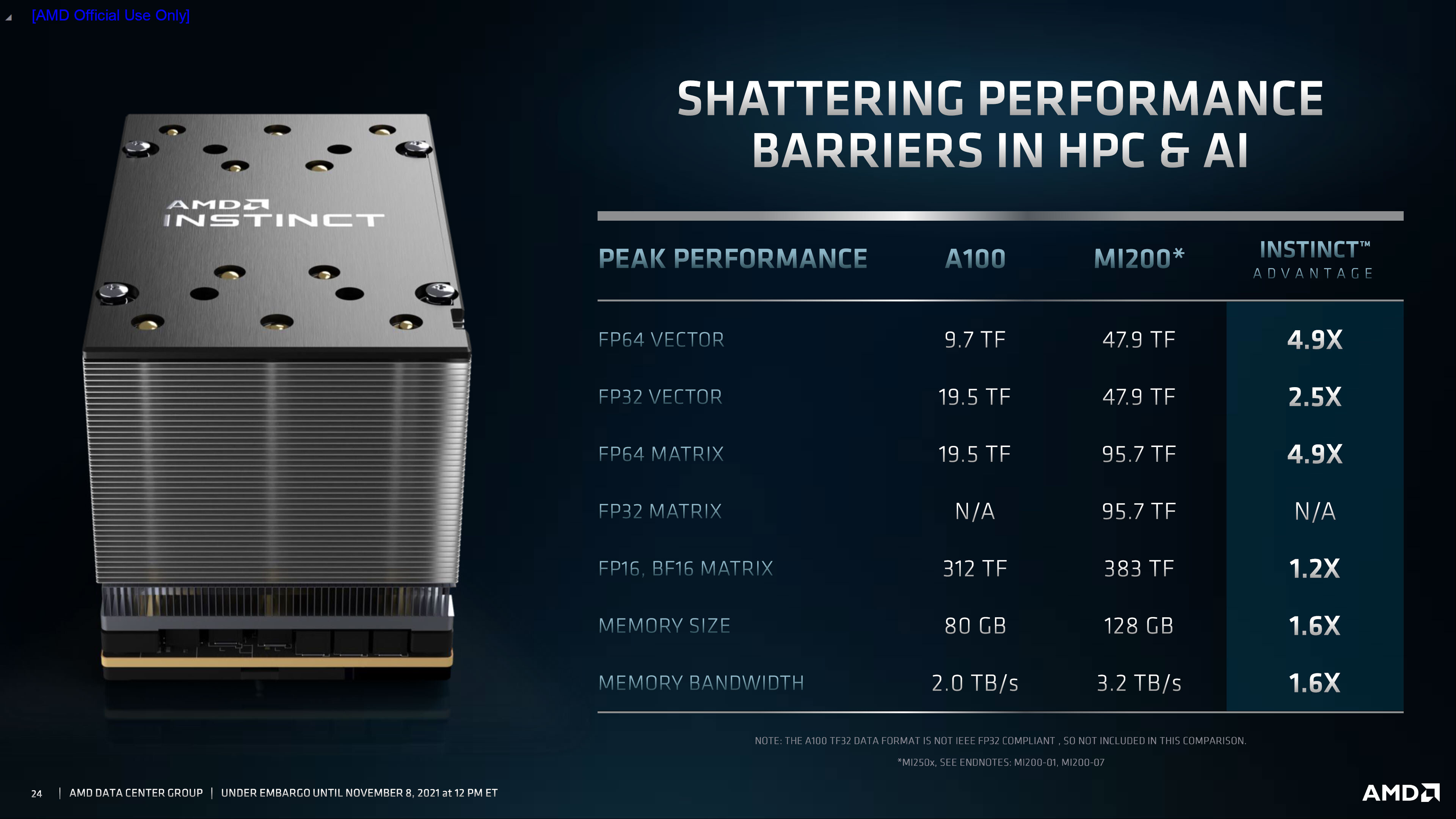
 AMD's MI250X accelerator features two compute dies with 58 Billion transistors built out of TSMC's 6 nm process. Each of these chips features a total of 110 Compute Units (CUs) for a total of 220 CUs on a single accelerator. The new CDNA2 architecture also incorporates new, improved Matrix Cores to the tune of 880 units (440 per chip). And as the MI250X is configured, that incredible amount of GPU power is paired with 128 GB of HBM2E memory, running at 3.2 TB/s. AMD's performance estimates against NVIDIA's current-gen A100 are blowouts. Compared to the A100, the MI250X is quoted as being: 4.9 times faster at FP64 vector compute; 2.5 times as fast in FP 32 Vector; 4.9 times faster in FP64 Matrix; a more meager 1.2 times faster performance on FP16 and BF16 Matrix operations; 1.6 times bigger memory capacity (128 GB on the MI 250X compared to the A100's 80 GB); and a 1.6 times faster memory bandwidth (though that's derived from the faster HBM2E memory).

 The two CDNA2 dies are linked together AMD's Infinity Fabric, which makes its debut on a graphics architecture. This link provides a series of 25 Gbps links offering up to 100 GB/s of bi-directional bandwidth between both GPUs. There are eight available links in the MI200's distribution module - built to the specifications of an OAM (OCP Accelerator Module, where OCP stands for "Open Compute Platform") configuration. In total 800 GB/s of bandwidth are available for on-the fly communication between the two chiplets. AMD already announced that a PCIe version of the MI200 is launching in the future, catering to those who just want drop-in replacements or upgrades.
 AMD's usage of TSMC's N6 fabrication technology can certainly account for part of the performance and die size improvement. As any manufacturer will do, AMD is employing yield optimizing efforts. This becomes clear when we look at the other product AMD is introducing alongside the MI250X: the MI250 accelerator. The MI250 takes a hit on computational resources by dropping from the MI250X's 110 CUs to 104 CUs per chiplet. That's actually the only change; it should be around 5% slower than the fully-enabled MI250X.
 All in all, the MI200 series is a marked improvement for AMD performance-wise. And yet, NVIDIA is sure to announce their own next-generation compute solution soon. How will the updated, CDNA2-powered MI200 series stand?
Sources:
Tom's Hardware, AnandTech


39 Comments on AMD Instinct MI200: Dual-GPU Chiplet; CDNA2 Architecture; 128 GB HBM2E
edit:
[USER=101241]blanarahul[/USER] [SIZE=4][B]beat me to it![/B][/SIZE]
A100 - 54 billion transistors
MI200 - 58 billion transistors (29 + 29), yet it runs circles around A100.You mean 22% faster is "barely faster"?
In reality? who know. The fact that Ampere have not that much less transistors for similar performance can mean that they choose to add a lot of in core memory. It's quite possible that MI200 is a hard to feed beast. Yes the high bandwidth can help, but still come with a latency disadvantage and will lead to a lot of unused cycles.
Vega problem was always about how hard it was to get maximum performance out of real workload.
Which in some applications will be seen as 1.6 TB/s, while other applications may see 3.2 TB/s. It depends on how you organize your data, and whether or not you can split your data into two memory-systems that are independent of each other.
Given that infinity fabric is like 400GB/s between the dies, your average-case (assuming 25% of your data in on the "far" memory and 75% of your data is in the "near" memory) is 2.0 TB/s, and only if one of the processors is near-idle. If you can split your data to be 100% in near-memory and not worry about the far-memory at all and have perfect parallelism, you can theoretically get to 3.2 TB.
Not that 1.6 TB/s is slow. But... given the "crossfire-like" setup here, I think its misleading to call this 3.2 TB of bandwidth.
Hmmm... I guess I'd "want" the OAM system, but who the heck would even sell you an OAM motherboard / system to play with? Those have to be incredibly expensive (thinking like $2000+ motherboards alone).
NVidia's DGX systems are $200,000+ computers. That's what I'd expect OAM-systems to cost at a minimum, maybe $200k to $1MM. Cache-coherent fabrics between CPU and GPU is just going to be expensive as all heck.
------------
Even the PCIe card is probably going to be outside the cost of any reasonable hobbyist.
And btw assuming anything is beyond someone you don't know is a bit lame, I do get to mess with some nice stuff at work, and home, it's just not always my own.
And is coincidentally why I build PC for others on the side , joy ,and obviously those 3dmark achievements won't get themselves.
Most likely, a "small person" would have access to these things if a cloud-provider started renting out some time to them. Either that, or university classes methinks. That's just how to make the $200,000 to $20,000,000 equipment work out for a community.
Its not so much "out of reach" as much as a community purchase. Either the community at your work, or some other learning-oriented community (technical school, university, colleges).
-----
I guess there are some very rich people out there who might be able to afford one of these things in their garage though. But if someone is that rich, I would hope that they join a university and allow the purchase to be used by students as well :cool: Acts of charity and all that, lol.
I'm not sure what your problem is actually as I said I want all sorts of shit I am ok with never owning, don't tell , your different aren't you!.?
I see your point though, recalling 3090's figures. :)A100 were sold in packs of 10, if I'm not mistaken, for $200k. I don't see why AMD would ask half of that sum for a vastly faster product.
The PCIe-versions won't have cache-coherency, and will have fewer links. Anyone who wants 2-or-fewer MI200s (or A100s) probably wants the PCIe version. The HGX A100 / OAM MI200 is really for customers who run 4x GPUs, 8x GPUs or more (which is probably why it makes sense to sell them in packs of 10).