News Posts matching #MI200

Return to Keyword Browsing

China Continues to Enhance AI Chip Self-Sufficiency, but High-End AI Chip Development Remains Constrained

Huawei's subsidiary HiSilicon has made significant strides in the independent R&D of AI chips, launching the next-gen Ascend 910B. These chips are utilized not only in Huawei's public cloud infrastructure but also sold to other Chinese companies. This year, Baidu ordered over a thousand Ascend 910B chips from Huawei to build approximately 200 AI servers. Additionally, in August, Chinese company iFlytek, in partnership with Huawei, released the "Gemini Star Program," a hardware and software integrated device for exclusive enterprise LLMs, equipped with the Ascend 910B AI acceleration chip, according to TrendForce's research.

TrendForce conjectures that the next-generation Ascend 910B chip is likely manufactured using SMIC's N+2 process. However, the production faces two potential risks. Firstly, as Huawei recently focused on expanding its smartphone business, the N+2 process capacity at SMIC is almost entirely allocated to Huawei's smartphone products, potentially limiting future capacity for AI chips. Secondly, SMIC remains on the Entity List, possibly restricting access to advanced process equipment.

New AI Accelerator Chips Boost HBM3 and HBM3e to Dominate 2024 Market

TrendForce reports that the HBM (High Bandwidth Memory) market's dominant product for 2023 is HBM2e, employed by the NVIDIA A100/A800, AMD MI200, and most CSPs' (Cloud Service Providers) self-developed accelerator chips. As the demand for AI accelerator chips evolves, manufacturers plan to introduce new HBM3e products in 2024, with HBM3 and HBM3e expected to become mainstream in the market next year.

The distinctions between HBM generations primarily lie in their speed. The industry experienced a proliferation of confusing names when transitioning to the HBM3 generation. TrendForce clarifies that the so-called HBM3 in the current market should be subdivided into two categories based on speed. One category includes HBM3 running at speeds between 5.6 to 6.4 Gbps, while the other features the 8 Gbps HBM3e, which also goes by several names including HBM3P, HBM3A, HBM3+, and HBM3 Gen2.

Major CSPs Aggressively Constructing AI Servers and Boosting Demand for AI Chips and HBM, Advanced Packaging Capacity Forecasted to Surge 30~40%

TrendForce reports that explosive growth in generative AI applications like chatbots has spurred significant expansion in AI server development in 2023. Major CSPs including Microsoft, Google, AWS, as well as Chinese enterprises like Baidu and ByteDance, have invested heavily in high-end AI servers to continuously train and optimize their AI models. This reliance on high-end AI servers necessitates the use of high-end AI chips, which in turn will not only drive up demand for HBM during 2023~2024, but is also expected to boost growth in advanced packaging capacity by 30~40% in 2024.

TrendForce highlights that to augment the computational efficiency of AI servers and enhance memory transmission bandwidth, leading AI chip makers such as Nvidia, AMD, and Intel have opted to incorporate HBM. Presently, Nvidia's A100 and H100 chips each boast up to 80 GB of HBM2e and HBM3. In its latest integrated CPU and GPU, the Grace Hopper Superchip, Nvidia expanded a single chip's HBM capacity by 20%, hitting a mark of 96 GB. AMD's MI300 also uses HBM3, with the MI300A capacity remaining at 128 GB like its predecessor, while the more advanced MI300X has ramped up to 192 GB, marking a 50% increase. Google is expected to broaden its partnership with Broadcom in late 2023 to produce the AISC AI accelerator chip TPU, which will also incorporate HBM memory, in order to extend AI infrastructure.

U.S. Government Restricts Export of AI Compute GPUs to China and Russia (Affects NVIDIA, AMD, and Others)

The U.S. Government has imposed restrictions on the export of AI compute GPUs to China and Russia without Government-authorization in the form of a waiver or a license. This impacts sales of products such as the NVIDIA A100, H100; AMD Instinct MI100, MI200; and the upcoming Intel "Ponte Vecchio," among others. The restrictions came to light when NVIDIA on Wednesday disclosed that it has received a Government notification about licensing requirements for export of its AI compute GPUs to Russia and China.

The notification doesn't specify the A100 and H100 by name, but defines AI inference performance thresholds to meet the licensing requirements. The Government wouldn't single out NVIDIA, and so competing products such as the AMD MI200 and the upcoming Intel Xe-HP "Ponte Vecchio" would fall within these restrictions. For NVIDIA, this is impacts $400 million in TAM, unless the Government licenses specific Russian and Chinese customers to purchase these GPUs from NVIDIA. Such trade restrictions usually come with riders to prevent resale or transshipment by companies outside the restricted region (eg: a distributor in a third waived country importing these chips in bulk and reselling them to these countries).

AMD Introduces Instinct MI210 Data Center Accelerator for Exascale-class HPC and AI in a PCIe Form-Factor

AMD today announced a new addition to the Instinct MI200 family of accelerators. Officially titled Instinct MI210 accelerator, AMD tries to bring exascale-class technologies to mainstream HPC and AI customers with this model. Based on CDNA2 compute architecture built for heavy HPC and AI workloads, the card features 104 compute units (CUs), totaling 6656 Streaming Processors (SPs). With a peak engine clock of 1700 MHz, the card can output 181 TeraFLOPs of FP16 half-precision peak compute, 22.6 TeraFLOPs peak FP32 single-precision, and 22.6 TFLOPs peak FP62 double-precision compute. For single-precision matrix (FP32) compute, the card can deliver a peak of 45.3 TFLOPs. The INT4/INT8 precision settings provide 181 TOPs, while MI210 can compute the bfloat16 precision format with 181 TeraFLOPs at peak.

The card uses a 4096-bit memory interface connecting 64 GBs of HMB2e to the compute silicon. The total memory bandwidth is 1638.4 GB/s, while memory modules run at a 1.6 GHz frequency. It is important to note that the ECC is supported on the entire chip. AMD provides an Instinct MI210 accelerator as a PCIe solution, based on a PCIe 4.0 standard. The card is rated for a TDP of 300 Watts and is cooled passively. There are three infinity fabric links enabled, and the maximum bandwidth of the infinity fabric link is 100 GB/s. Pricing is unknown; however, availability is March 22nd, which is the immediate launch date.

AMD places this card directly aiming at NVIDIA A100 80 GB accelerator as far as the targeted segment, with emphasis on half-precision and INT4/INT8 heavy applications.

AMD Instinct MI200: Dual-GPU Chiplet; CDNA2 Architecture; 128 GB HBM2E

AMD today announced the debut of its 6 nm CDNA2 (Compute-DNA) architecture in the form of the MI200 family. The new, dual-GPU chiplet accelerator aims to lead AMD into a new era of High Performance Computing (HPC) applications, the high margin territory it needs to compete in for continued, sustainable growth. To that end, AMD has further improved on a matured, compute-oriented architecture born with Graphics Core Next (GCN) - and managed to improve performance while reducing total die size compared to its MI100 family.

AMD Readies MI250X Compute Accelerator with 110 CUs and 128 GB HBM2E

AMD is preparing an update to its compute accelerator lineup with the new MI250X. Based on the CDNA2 architecture, and built on existing 7 nm node, the MI250X will be accompanied by a more affordable variant, the MI250. According to leaks put out by ExecutableFix, the MI250X packs a whopping 110 compute units (7,040 stream processors), running at 1.70 GHz. The package features 128 GB of HBM2E memory, and a package TDP of 500 W. As for speculative performance numbers, it is expected to offer double-precision (FP64) throughput of 47.9 TFLOP/s, ditto full-precision (FP32), and 383 TFLOP/s half-precision (FP16 and BFLOAT16). AMD's MI200 "Aldebaran" family of compute accelerators are expected to square off against Intel's "Ponte Vecchio" Xe-HPC, and NVIDIA Hopper H100 accelerators in 2022.

Intel Ponte Vecchio Early Silicon Puts Out 45 TFLOPs FP32 at 1.37 GHz, Already Beats NVIDIA A100 and AMD MI100

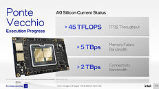
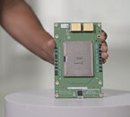
Intel in its 2021 Architecture Day presentation put out fine technical details of its Xe HPC Ponte Vecchio accelerator, including some [very] preliminary performance claims for its current A0-silicon-based prototype. The prototype operates at 1.37 GHz, but achieves out at least 45 TFLOPs of FP32 throughput. We calculated the clock speed based on simple math. Intel obtained the 45 TFLOPs number on a machine running a single Ponte Vecchio OAM (single MCM with two stacks), and a Xeon "Sapphire Rapids" CPU. 45 TFLOPs sees the processor already beat the advertised 19.5 TFLOPs of the NVIDIA "Ampere" A100 Tensor Core 40 GB processor. AMD isn't faring any better, with its production Instinct MI100 processor only offering 23.1 TFLOPs FP32.

AMD Zen 4 and RDNA3 Confirmed for 2022, Zen 3 Refresh

AMD CEO Dr Lisa Su, in the company's Q2-2021 financial results call, confirmed that the company is on-track to launch the Zen 4 CPU microarchitecture and RDNA3 graphics architecture, in 2022. Zen 4 would herald the first major desktop platform change since the original Zen architecture, with the introduction of a new CPU socket, and support for DDR5 memory. The RDNA3 graphics architecture, meanwhile, is expected to nearly triple SIMD resources over the previous generation, and introduce even more fixed-function hardware for raytracing.

In the meantime, AMD is preparing a counter to Intel's 12th Gen Core "Alder Lake-S" processor, in the form of Zen 3 with 3D Vertical Cache, which is also being referred to as the Zen 3+ architecture. These processors feature additional last-level cache, and the company claims a 15% gaming performance uplift, which should help it close the gaming performance gap with Intel, and win on sheer core-count of its big cores. It remains to be seen if Zen 3+ remains on Socket AM4 or if it debuts AM5, as AMD will be under pressure to match "Alder Lake" in platform I/O, which includes DDR5. Dr Su also confirmed that AMD has started shipping the Instinct MI200 "Aldebaran" compute accelerator based on the CDNA2 architecture. AMD's first MCM GPU with two logic dies, "Aldebaran" takes the fight to NVIDIA's top A100 series compute accelerators, and has already scored wins with ongoing HPC/supercomputing projects.

AMD MI200 "Aldebaran" Memory Size of 128GB Per Package Confirmed

The 128 GB per package memory size of AMD's upcoming Instinct MI200 HPC accelerator was confirmed, in a document released by Pawsey SuperComputing Centre, a Perth, Australia-based supercomputing firm that's popular with mineral prospecting companies located there. The company is currently working on Setonix, a 50-petaFLOP supercomputer being put together by HP Enterprise, which combines over 750 next-generation "Aldebaran" GPUs (referenced only as "AMD MI-Next GPUs"); and over 200,000 AMD EPYC "Milan" processor cores (the actual processor package count would be lower, and depend on the various core configs the builder is using).

The Pawsey document mentions 128 GB as the per-GPU memory. This corresponds with the rumored per-package memory of "Aldebaran." Recently imagined by Locuza_, an enthusiast who specializes in annotation of logic silicon dies, "Aldebaran" is a multi-chip module of two logic dies and eight HBM2E stacks. Each of the two logic dies, or chiplets, has 8,192 CDNA2 stream processors that add up to 16,384 on the package; and each of the two dies is wired to four HBM2E stacks over a 4096-bit memory bus. These are 128 Gbit (16 GB) stacks, so we have 64 GB memory per logic die, and 128 GB on the package. Find other drool worthy specs of the Pawsey Setonix in the screengrab below.

AMD CDNA2 "Aldebaran" MI200 HPC Accelerator with 256 CU (16,384 cores) Imagined

AMD Instinct MI200 will be an important product for the company in the HPC and AI supercomputing market. It debuts the CDNA2 compute architecture, and is based on a multi-chip module (MCM) codenamed "Aldebaran." PC enthusiast Locuza, who conjures highly detailed architecture based on public information, imagined what "Aldebaran" could look like. The MCM contains two logic dies, and eight HBM2E stacks. Each of the two dies has a 4096-bit HBM2E interface, which talks to 64 GB of memory (128 GB per package). A silicon interposer provides microscopic wiring among the ten dies.

Each of the two logic dies, or chiplets, has sixteen shader engines that have 16 compute units (CU), each. The CDNA2 compute unit is capable of full-rate FP64, packed FP32 math, and Matrix Engines V2 (fixed function hardware for matrix multiplication, accelerating DNN building, training, and AI inference). With 128 CUs per chiplet, assuming the CDNA2 CU has 64 stream processors, one arrives at 8,192 SP. Two such dies add up to a whopping 16,384, more than three times that of the "Navi 21" RDNA2 silicon. Each die further features its independent PCIe interface, and XGMI (AMD's rival to CXL), an interconnect designed for high-density HPC scenarios. A rudimentary VCN (Video CoreNext) component is also present. It's important to note here, that the CDNA2 CU, as well as the "Aldebaran" MCM itself, doesn't have a dual-use as a GPU, since it lacks much of the hardware needed for graphics processing. The MI200 is expected to launch later this year.

AMD Confirms CDNA2 Instinct MI200 GPU Will Feature at Least Two Dies in MCM Design

Today we've got the first genuine piece of information that confirms AMD's MCM approach to CDNA2, the next-gen compute architecture meant for ML/HPC/Exascale computing. This comes courtesy of a Linux kernel update, where AMD engineers annotated the latest Linux kernel patch with some considerations specific for their upcoming Aldebaran, CDNA2-based compute cards. Namely, the engineers clarify the existence of a "Die0" and a "Die1", where power data fetching should be allocated to Die0 of the accelerator card - and that the power limit shouldn't be set on the secondary die.

This confirms that Aldebaran will be made of at least two CDNA2 compute dies, and as (almost) always in computing, one seems to be tasked with general administration of both compute dies. It is unclear as of yet whether the HBM2 memory controller will be allocated to the primary die, or if there will be an external I/O die (much like in Zen) that AMD can leverage for off-chip communication. AMD's approach to CDNA2 will eventually find its way (in an updated form) for AMD's consumer-geared next-generation graphics architecture with RDNA3.

AMD Instinct MI200 "Aldebaran" to Launch Later This Year

AMD's next-generation HPC accelerator card, the Instinct MI200, is expected to launch later this year. CEO Dr Lisa Su, speaking at a financial event hosted by JPMorgan stated that the company would launch the next-generation of CDNA architecture this year. The card debuts the company's new CDNA2 compute architecture, and is on its way to supercomputers already announced. The Instinct MI200 HPC accelerator card is based on the new "Aldebaran" compute accelerator package, which is a multi-chip module of not just the compute silicon and memory dies; but one that has multiple compute dies.

AMD Instinct MI200 to Launch This Year with MCM Design

AMD is slowly preparing the next-generation of its compute-oriented flagship graphics card design called Instinct MI200 GPU. It is the card of choice for the exascale Frontier supercomputer, which is expected to make a debut later this year at the Oak Ridge Leadership Computing Facility. With the supercomputer planned for the end of this year, AMD Instinct MI200 is also going to get launched eight a bit before or alongside it. The Frontier exascale supercomputer is supposed to bring together AMD's next-generation Trento EPYC CPUs with Instinct MI200 GPU compute accelerators. However, it seems like AMD will utilize some new technologies for the making of this supercomputer. While we do not know what Trento EPYC CPUs will look like, it seems like Instinct MI200 GPU is going to feature a multi-chip-module (MCM) design with the new CDNA 2 GPU architecture. With this being the only information about the GPU, we have to wait a bit to find out more details.
AMD CDNA Die
Return to Keyword Browsing
Oct 31st, 2024 19:27 EDT change timezone

New Forum Posts

Popular Reviews

Controversial News Posts