Tuesday, November 29th 2022

Samsung Develops GDDR6W Memory Standard: Double the Bandwidth and Density of GDDR6 Through Packaging Innovations
As advanced graphics and display technologies develop, they are blurring the lines between metaverse and our everyday experience. Much of this important shift is being made possible by the advancement of memory solutions designed for graphics products. One of the biggest challenges for improving virtual reality is taking the complexities of real-world objects and environments and recreating them in a virtual space. Doing so requires massive memory and increased computing power. At the same time, the benefits of creating more true-to-life metaverse will be far reaching, including real-life simulations of complicated scenarios and more, sparking innovation across a number of industries.
This is the central idea behind one of the most popular concepts in virtual reality: digital twin. A digital twin is a virtual representation of an object or space. Updated in real-time in accordance with the actual environment, a digital twin spans the lifecycle of its source and uses simulation, machine learning and reasoning to help decision-making. While until recently this was not feasible proposition due to limitations on data processing and transference, digital twins are now gaining traction thanks to availability of high bandwidth technologies.

 Like other tech innovations, the gaming industry thrives on constant innovation, with new updates in speed and performance driving the market forward year after year. Thanks to the development of technologies like Ray Tracing in 3D rendering, which traces the reflection of light in a given scene, graphics in high-end AAA gaming are becoming hyper realistic and increasingly immersive.
Ray tracing enables the collection of light information to determine the color of each pixel through real-time calculation. This kind of calculation requires near-simultaneous computation of substantial amounts of data—between 60 to 140 pages worth for one second of an in-game scene. What's more, display quality is rising fast, with resolutions rapidly transitioning from 4K to 8K standard, while frame buffers are increasing to expand two times more than existing ones in response. That's why high capacity and high bandwidth are essential to meeting the growing memory demand as games continue to develop.
Developing 'GDDR6W' Graphics Memory, with Doubled Capacity and Performance Based on the Cutting-edge Fan-Out Wafer-Level Packaging (FOWLP) Technology
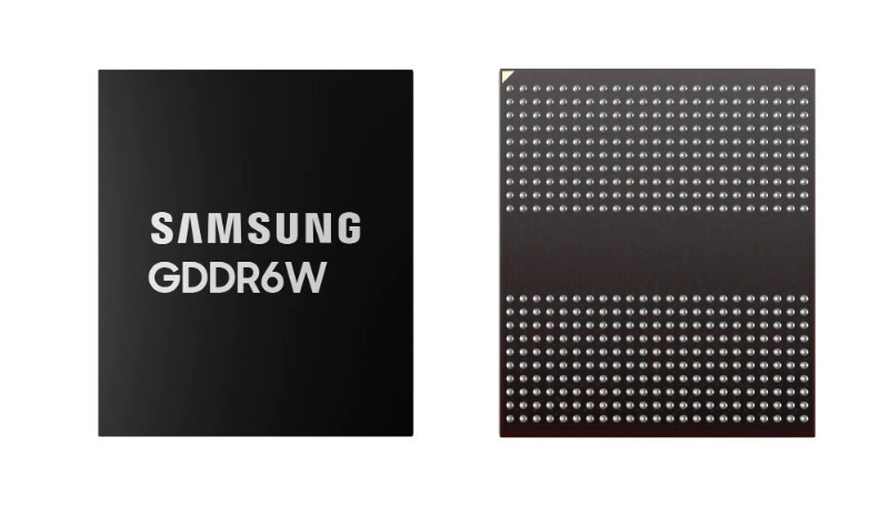
High performance, high capacity and high bandwidth memory solutions are helping bring the virtual realm to a closer match with reality. To meet this growing market demand, Samsung Electronics has developed GDDR6W (x64): the industry's first next-generation graphics DRAM technology.
GDDR6W builds on Samsung's GDDR6 (x32) products by introducing a Fan-Out Wafer-Level Packaging (FOWLP) technology, drastically increasing memory bandwidth and capacity.
Since its launch, GDDR6 has already seen significant improvements. Last July, Samsung developed a 24 Gbps GDDR6 memory, the industry's fastest graphics DRAM. GDDR6W doubles that bandwidth (performance) and capacity while remaining the identical size of GDDR6. Thanks to the unchanged footprint, new memory chips can easily be put into the same production processes customers have used for GDDR6, with the use of the FOWLP construction and stacking technology, cutting manufacturing time and costs.
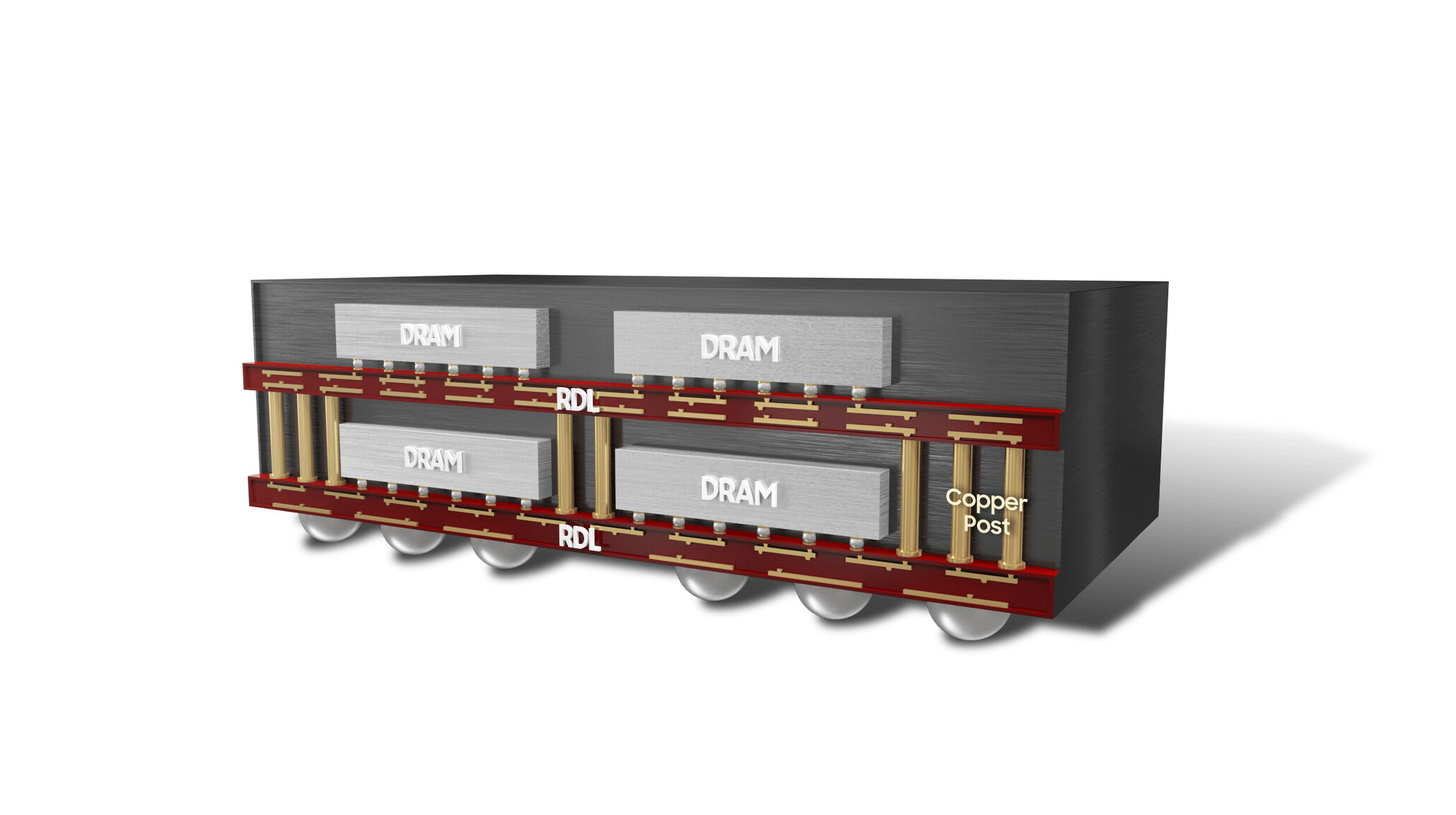
As shown in the picture below, since it can be equipped with twice as many memory chips in an identical size package, the graphic DRAM capacity has increased from 16Gb to 32Gb, while bandwidth and the number of I/Os has doubled from 32 to 64. In other words, the area required for memory has been reduced 50% compared to previous models.
Generally, the size of a package increases as more chips are stacked. But there are physical factors that limit the maximum height of a package. What's more, though stacking chips increases capacity, there is a trade-off in heat dissipation and performance. In order to overcome these trade-offs, we've applied our FOWLP technology to GDDR6W.
FOWLP technology directly mounts memory die on a silicon wafer, instead of a PCB. In doing so, RDL (Re-distribution layer) technology is applied, enabling much finer wiring patterns. Additionally, as there's no PCB involved, it reduces the thickness of the package and improves heat dissipation.
The height of the FOWLP-based GDDR6W is 0.7 mm - 36% slimmer than the previous package with a height of 1.1 mm. And despite the chip being multi-layered, it still offers the same thermal properties and performance as the existing GDDR6. Unlike GDDR6, however, the bandwidth of the FOWLP-based GDDR6W can be doubled thanks to the expanded I/O per single package.
Packaging refers to the process of cutting fabricated wafers into semiconductor shapes or connecting wires. In the industry, this is known as a 'back-end process.' While the semiconductor industry has continuously developed towards scaling circuits as much as possible during the front-end process, packaging technology is becoming more and more important as the industry approaches the physical limits of chip sizes limits. That's why Samsung is using its 3D IC package technology in GDDR6W, creating a single package by stacking a variety of chips in a wafer state. This is one of many innovations planned to make advanced packaging for GDDR6W faster and more efficient.
The newly developed GDDR6W technology can support HBM-level bandwidth at a system level. HBM2E has a system-level bandwidth of 1.6 TB/s based on 4K system-level I/O and a 3.2 Gbps transmission rate per pin. GDDR6W, on the other hand, can produce a bandwidth of 1.4 TB/s based on 512 system-level I/O and a transmission rate of 22Gpbs per pin. Furthermore, since GDDR6W reduces the number of I/O to about 1/8 compared with using HBM2E, it removes the necessity of using microbumps. That makes it more cost-effective without the need for an interposer layer.
"By applying an advanced packaging technology to GDDR6, GDDR6W delivers twice the memory capacity and performance of similar-sized packages," said CheolMin Park, Vice President of New Business Planning, Samsung Electronics Memory Business. "With GDDR6W, we're able to foster differentiated memory products that can satisfy various customer needs - a major step towards securing our leadership in the market."
Samsung Electronics completed the JEDEC standardization for GDDR6W products in the second quarter of this year. It has also announced that it will expand the application of GDDR6W to small form factor devices such as notebooks as well as new high-performance accelerators used for AI and HPC applications, through cooperation with its GPU partners.
This is the central idea behind one of the most popular concepts in virtual reality: digital twin. A digital twin is a virtual representation of an object or space. Updated in real-time in accordance with the actual environment, a digital twin spans the lifecycle of its source and uses simulation, machine learning and reasoning to help decision-making. While until recently this was not feasible proposition due to limitations on data processing and transference, digital twins are now gaining traction thanks to availability of high bandwidth technologies.

Ray tracing enables the collection of light information to determine the color of each pixel through real-time calculation. This kind of calculation requires near-simultaneous computation of substantial amounts of data—between 60 to 140 pages worth for one second of an in-game scene. What's more, display quality is rising fast, with resolutions rapidly transitioning from 4K to 8K standard, while frame buffers are increasing to expand two times more than existing ones in response. That's why high capacity and high bandwidth are essential to meeting the growing memory demand as games continue to develop.
Developing 'GDDR6W' Graphics Memory, with Doubled Capacity and Performance Based on the Cutting-edge Fan-Out Wafer-Level Packaging (FOWLP) Technology
High performance, high capacity and high bandwidth memory solutions are helping bring the virtual realm to a closer match with reality. To meet this growing market demand, Samsung Electronics has developed GDDR6W (x64): the industry's first next-generation graphics DRAM technology.
GDDR6W builds on Samsung's GDDR6 (x32) products by introducing a Fan-Out Wafer-Level Packaging (FOWLP) technology, drastically increasing memory bandwidth and capacity.
Since its launch, GDDR6 has already seen significant improvements. Last July, Samsung developed a 24 Gbps GDDR6 memory, the industry's fastest graphics DRAM. GDDR6W doubles that bandwidth (performance) and capacity while remaining the identical size of GDDR6. Thanks to the unchanged footprint, new memory chips can easily be put into the same production processes customers have used for GDDR6, with the use of the FOWLP construction and stacking technology, cutting manufacturing time and costs.
As shown in the picture below, since it can be equipped with twice as many memory chips in an identical size package, the graphic DRAM capacity has increased from 16Gb to 32Gb, while bandwidth and the number of I/Os has doubled from 32 to 64. In other words, the area required for memory has been reduced 50% compared to previous models.
Generally, the size of a package increases as more chips are stacked. But there are physical factors that limit the maximum height of a package. What's more, though stacking chips increases capacity, there is a trade-off in heat dissipation and performance. In order to overcome these trade-offs, we've applied our FOWLP technology to GDDR6W.
FOWLP technology directly mounts memory die on a silicon wafer, instead of a PCB. In doing so, RDL (Re-distribution layer) technology is applied, enabling much finer wiring patterns. Additionally, as there's no PCB involved, it reduces the thickness of the package and improves heat dissipation.
The height of the FOWLP-based GDDR6W is 0.7 mm - 36% slimmer than the previous package with a height of 1.1 mm. And despite the chip being multi-layered, it still offers the same thermal properties and performance as the existing GDDR6. Unlike GDDR6, however, the bandwidth of the FOWLP-based GDDR6W can be doubled thanks to the expanded I/O per single package.
Packaging refers to the process of cutting fabricated wafers into semiconductor shapes or connecting wires. In the industry, this is known as a 'back-end process.' While the semiconductor industry has continuously developed towards scaling circuits as much as possible during the front-end process, packaging technology is becoming more and more important as the industry approaches the physical limits of chip sizes limits. That's why Samsung is using its 3D IC package technology in GDDR6W, creating a single package by stacking a variety of chips in a wafer state. This is one of many innovations planned to make advanced packaging for GDDR6W faster and more efficient.
The newly developed GDDR6W technology can support HBM-level bandwidth at a system level. HBM2E has a system-level bandwidth of 1.6 TB/s based on 4K system-level I/O and a 3.2 Gbps transmission rate per pin. GDDR6W, on the other hand, can produce a bandwidth of 1.4 TB/s based on 512 system-level I/O and a transmission rate of 22Gpbs per pin. Furthermore, since GDDR6W reduces the number of I/O to about 1/8 compared with using HBM2E, it removes the necessity of using microbumps. That makes it more cost-effective without the need for an interposer layer.
"By applying an advanced packaging technology to GDDR6, GDDR6W delivers twice the memory capacity and performance of similar-sized packages," said CheolMin Park, Vice President of New Business Planning, Samsung Electronics Memory Business. "With GDDR6W, we're able to foster differentiated memory products that can satisfy various customer needs - a major step towards securing our leadership in the market."
Samsung Electronics completed the JEDEC standardization for GDDR6W products in the second quarter of this year. It has also announced that it will expand the application of GDDR6W to small form factor devices such as notebooks as well as new high-performance accelerators used for AI and HPC applications, through cooperation with its GPU partners.
30 Comments on Samsung Develops GDDR6W Memory Standard: Double the Bandwidth and Density of GDDR6 Through Packaging Innovations
512-bit bus is fine, but wouldn't 768-bit be possible with this ?
Theoretical 32 GB 512-bit @ 22 GHz = 1408 GB/sec and needs 8 (which is 4 less) memory chips
Perhaps they will be able to translate this tech to their m.2's, so we can FINALLY get some seriously higher capacity drives instead of the puny 1, 2, 4, & 8TB ones that we have to settle for ATM
This tech is more about packaging than pure speed. A desktop card will be able to use half the memory chip for the same bus size. They will be able to use a smaller PCB, a smaller heatsink and simplify the packaging. I don't think that it will be a huge benefits on that side except maybe for low profile cards and similar stuff.
I think the real benefits will be on mobile GPU. they will be able to do much denser packaging leaving more room for cooling or other stuff.You would also need 8 MCD, and there is no room to connect that to Navi31, it would require a larger chip. And you still have to face the increased cost for routing a 512 bit bus. (Plus on RDNA3, the added cost of routing 2 more MCD to the CGD).
Also NAND is already stacked, in a MASSIVE way, If you buy an 8GB M2 SSD, it will likely be using NAND that is 144 layers.!
I recognize you're just copy/pasting from Samsung, but... wtf is going on here? Did Facebook / Meta / Mark Zuckerberg just pay a ton of ad money to Samsung (and Fidelity for that matter: institutional.fidelity.com/app/funds-and-products/etf/snapshot/FIIS_ETF_FMET/fidelity-metaverse-etf.html) ??
There's clearly a media blitz going on trying to make Metaverse a thing. It feels very astroturfed / fake to me though. Anyone else getting this feeling?
--------
Anyway, GDDR6W, faster better than GDDR6x (EDIT: Woops, better than GDDR6. Seems like GDDR6x might be a "different branch"?? Maybe incompatible with this new packaging format??). Got it. Good news for GPU makers I guess, but... its a stretch to paint this as part of the "metaverse" (whatever that is...). I'm cool with the overall information being presented, but I'm just... curious... where this metaverse social-media blitz is coming from.
Modern and less modern DRAM uses the latter. I found these sources from 2007 that mention through-silicon vias as the new tech versus wire bonding as the old tech used to connect the dies:
phys.org/news/2007-04-samsung-highly-efficient-stacking-dram.html
bit-tech.net/reviews/tech/memory/the_secrets_of_pc_memory_part_2/6/
Monolithic stacking in DRAM is still on the drawing board, I'm sure a lot of money is being poured into research, and it will be a breakthrough when it arrives, but it's not about to arrive soon.
I agree that each RDNA3 MCD has a 64-bit wide memory bus and it's difficult to fit more than 6 on a single package. However, future RDNA4 MCD can have 96-bit/128-bit wide memory bus. That's what GDDR6W is targeting anyway.Moar bandwidth comes at an increased cost anyway. That's expected.
On another note, Nvidia would have benefitted a lot from something like this in 2020 with Ampere (in terms of VRAM size).
RTX 3080 came with 320-bit 19 GHz = 760 GB/sec bandwidth but only had 10 GB capacity.
Considering GDDR6 was at 14 GHz in Ampere, 448-bit 14 GHz = 784 GB/sec bandwidth with 14 GB VRAM size.