News Posts matching #CoWoS

Return to Keyword Browsing

SK hynix Strengthens AI Memory Leadership & Partnership With Host at the TSMC 2024 Tech Symposium

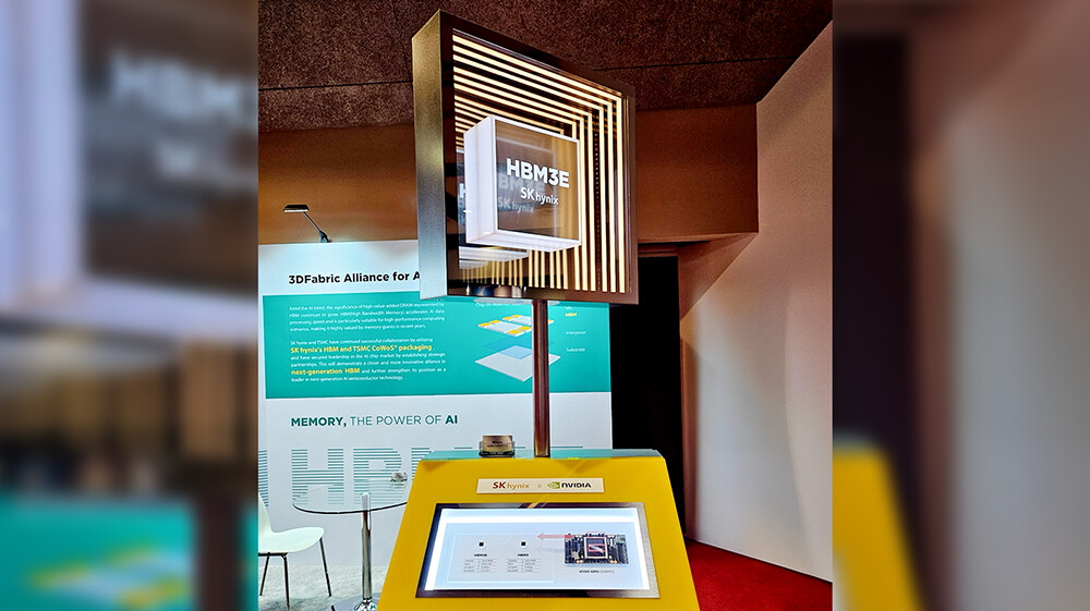
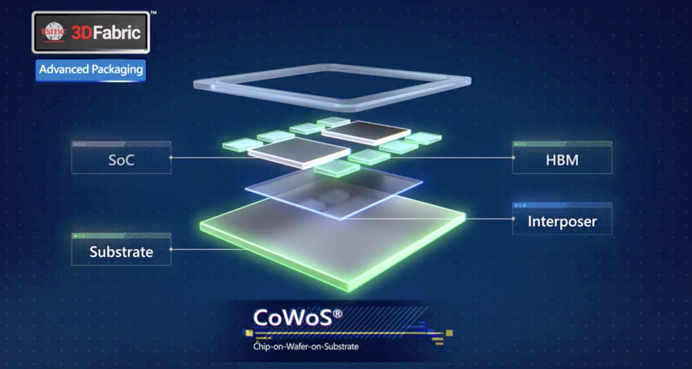
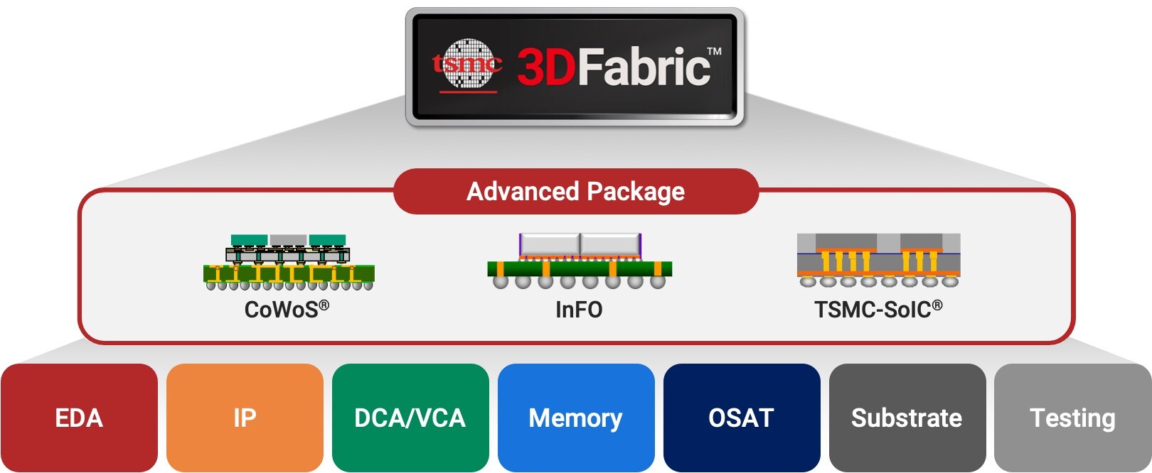
SK hynix showcased its next-generation technologies and strengthened key partnerships at the TSMC 2024 Technology Symposium held in Santa Clara, California on April 24. At the event, the company displayed its industry-leading HBM AI memory solutions and highlighted its collaboration with TSMC involving the host's CoWoS advanced packaging technology.

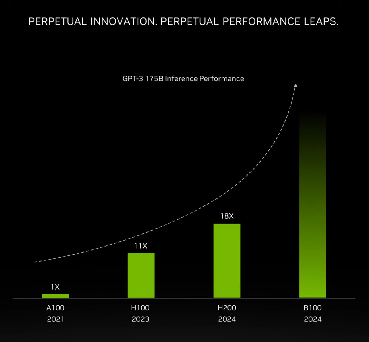
TSMC, a global semiconductor foundry, invites its major partners to this annual conference in the first half of each year so they can share their new products and technologies. Attending the event under the slogan "Memory, the Power of AI," SK hynix received significant attention for presenting the industry's most powerful AI memory solution, HBM3E. The product has recently demonstrated industry-leading performance, achieving input/output (I/O) transfer speed of up to 10 gigabits per second (Gbps) in an AI system during a performance validation evaluation.

TSMC Celebrates 30th North America Technology Symposium with Innovations Powering AI with Silicon Leadership

TSMC today unveiled its newest semiconductor process, advanced packaging, and 3D IC technologies for powering the next generation of AI innovations with silicon leadership at the Company's 2024 North America Technology Symposium. TSMC debuted the TSMC A16 technology, featuring leading nanosheet transistors with innovative backside power rail solution for production in 2026, bringing greatly improved logic density and performance. TSMC also introduced its System-on-Wafer (TSMC-SoW) technology, an innovative solution to bring revolutionary performance to the wafer level in addressing the future AI requirements for hyperscaler datacenters.

This year marks the 30th anniversary of TSMC's North America Technology Symposium, and more than 2,000 attended the event, growing from less than 100 attendees 30 years ago. The North America Technology Symposium in Santa Clara, California kicks off TSMC Technology Symposiums around the world in the coming months. The symposium also features an "Innovation Zone," designed to highlight the technology achievements of our emerging start-up customers.

SK hynix Collaborates with TSMC on HBM4 Chip Packaging

SK hynix Inc. announced today that it has recently signed a memorandum of understanding with TSMC for collaboration to produce next-generation HBM and enhance logic and HBM integration through advanced packaging technology. The company plans to proceed with the development of HBM4, or the sixth generation of the HBM family, slated to be mass-produced from 2026, through this initiative.

SK hynix said the collaboration between the global leader in the AI memory space and TSMC, a top global logic foundry, will lead to more innovations in HBM technology. The collaboration is also expected to enable breakthroughs in memory performance through trilateral collaboration between product design, foundry, and memory provider. The two companies will first focus on improving the performance of the base die that is mounted at the very bottom of the HBM package. HBM is made by stacking a core DRAM die on top of a base die that features TSV technology, and vertically connecting a fixed number of layers in the DRAM stack to the core die with TSV into an HBM package. The base die located at the bottom is connected to the GPU, which controls the HBM.

Demand for NVIDIA's Blackwell Platform Expected to Boost TSMC's CoWoS Total Capacity by Over 150% in 2024

NVIDIA's next-gen Blackwell platform, which includes B-series GPUs and integrates NVIDIA's own Grace Arm CPU in models such as the GB200, represents a significant development. TrendForce points out that the GB200 and its predecessor, the GH200, both feature a combined CPU+GPU solution, primarily equipped with the NVIDIA Grace CPU and H200 GPU. However, the GH200 accounted for only approximately 5% of NVIDIA's high-end GPU shipments. The supply chain has high expectations for the GB200, with projections suggesting that its shipments could exceed millions of units by 2025, potentially making up nearly 40 to 50% of NVIDIA's high-end GPU market.

Although NVIDIA plans to launch products such as the GB200 and B100 in the second half of this year, upstream wafer packaging will need to adopt more complex and high-precision CoWoS-L technology, making the validation and testing process time-consuming. Additionally, more time will be required to optimize the B-series for AI server systems in aspects such as network communication and cooling performance. It is anticipated that the GB200 and B100 products will not see significant production volumes until 4Q24 or 1Q25.

Nvidia CEO Reiterates Solid Partnership with TSMC

One key takeaway from the ongoing GTC is that Nvidia's AI empire has taken shape with strong partnerships from TSMC and other Taiwanese makers, such as those major server ODMs.

According to the news report from the technology-focused media DIGITIMES Asia, during his keynote at GTC on March 18, Huang underscored his company's partnerships with TSMC, as well as the supply chain in Taiwan. Speaking to the press later, Huang said Nvidia will have a very strong demand for CoWoS, the advanced packaging services TSMC offers.

TSMC Reportedly Investing $16 Billion into New CoWoS Facilities

TSMC is experiencing unprecedented demand from AI chip customers—unnamed parties have (fancifully) requested the construction of entirely new fabrication facilities. Taiwan's leading semiconductor contract manufacturer seems to concentrating on "sensible" expansions, mainly in the area of CoWoS packaging output—according to an Economic Daily report, company leadership and local government were negotiating over the construction of four new advanced packaging plants. Insiders propose that plans have been revised—an investment in excess of 500 billion yuan ($16 billion) will enable the founding of six new CoWoS-focused facilities. TSMC is expected to make an official announcement next month—industry moles reckon that construction work will start in April. Two (of the six total) advanced packaging plants could become fully operational before the conclusion of 2024.

Lately, TSMC has initiated an ambitious recruitment drive—targeting around 6000 new workers. A touring entity is tasked with the attraction of "talents with high enthusiasm for semiconductors." The majority of new recruits are likely heading to new or expanded Taiwan-based facilities. The Economic Daily report proposes that Chiayi City's technological hub will play host to TSMC's new CoWoS packaging plants. A DigiTimes Asia news piece (from January) posited that TSMC leadership anticipates CoWoS output reaching 44,000 units by the end of 2024. This predicted tally could grow, thanks to the (rumored) activation of additional factories. CoWoS packaging is considered to be a vital aspect of AI accelerators—insiders believe that TSMC's latest investment will boost production of NVIDIA H100 GPUs. The combined output of six new CoWoS plants will assist greatly in the creation of next-gen B100 chips.

NVIDIA B100 "Blackwell" AI GPU Technical Details Leak Out

Jensen Huang's opening GTC 2024 keynote is scheduled to happen tomorrow afternoon (13:00 Pacific time)—many industry experts believe that the NVIDIA boss will take the stage and formally introduce his company's B100 "Blackwell" GPU architecture. An enlightened few have been treated to preview (AI and HPC) units—including Dell's CEO, Jeff Clarke—but pre-introduction leaks have not flowed out. Team Green is likely enforcing strict conditions upon a fortunate selection of trusted evaluators, within a pool of ecosystem partners and customers.

Today, a brave soul has broken that silence—tech tipster, AGF/XpeaGPU, fears repercussions from the leather-jacketed one. They revealed a handful of technical details, a day prior to Team Green's highly anticipated unveiling: "I don't want to spoil NVIDIA B100 launch tomorrow, but this thing is a monster. 2 dies on (TSMC) CoWoS-L, 8x8-Hi HBM3E stacks for 192 GB of memory." They also crystal balled an inevitable follow-up card: "one year later, B200 goes with 12-Hi stacks and will offer a beefy 288 GB. And the performance! It's... oh no Jensen is there... me run away!" Reuters has also joined in on the fun, with some predictions and insider information: "NVIDIA is unlikely to give specific pricing, but the B100 is likely to cost more than its predecessor, which sells for upwards of $20,000." Enterprise products are expected to arrive first—possibly later this year—followed by gaming variants, maybe months later.

HBM3 Initially Exclusively Supplied by SK Hynix, Samsung Rallies Fast After AMD Validation

TrendForce highlights the current landscape of the HBM market, which as of early 2024, is primarily focused on HBM3. NVIDIA's upcoming B100 or H200 models will incorporate advanced HBM3e, signaling the next step in memory technology. The challenge, however, is the supply bottleneck caused by both CoWoS packaging constraints and the inherently long production cycle of HBM—extending the timeline from wafer initiation to the final product beyond two quarters.

The current HBM3 supply for NVIDIA's H100 solution is primarily met by SK hynix, leading to a supply shortfall in meeting burgeoning AI market demands. Samsung's entry into NVIDIA's supply chain with its 1Znm HBM3 products in late 2023, though initially minor, signifies its breakthrough in this segment.

TSMC Plans to Put a Trillion Transistors on a Single Package by 2030

During the recent IEDM conference, TSMC previewed its process roadmap for delivering next-generation chip packages packing over one trillion transistors by 2030. This aligns with similar long-term visions from Intel. Such enormous transistor counts will come through advanced 3D packaging of multiple chipsets. But TSMC also aims to push monolithic chip complexity higher, ultimately enabling 200 billion transistor designs on a single die. This requires steady enhancement of TSMC's planned N2, N2P, N1.4, and N1 nodes, which are slated to arrive between now and the end of the decade. While multi-chipset architectures are currently gaining favor, TSMC asserts both packaging density and raw transistor density must scale up in tandem. Some perspective on the magnitude of TSMC's goals include NVIDIA's 80 billion transistor GH100 GPU—among today's largest chips, excluding wafer-scale designs from Cerebras.

Yet TSMC's roadmap calls for more than doubling that, first with over 100 billion transistor monolithic designs, then eventually 200 billion. Of course, yields become more challenging as die sizes grow, which is where advanced packaging of smaller chiplets becomes crucial. Multi-chip module offerings like AMD's MI300X and Intel's Ponte Vecchio already integrate dozens of tiles, with PVC having 47 tiles. TSMC envisions this expansion to chip packages housing more than a trillion transistors via its CoWoS, InFO, 3D stacking, and many other technologies. While the scaling cadence has recently slowed, TSMC remains confident in achieving both packaging and process breakthroughs to meet future density demands. The foundry's continuous investment ensures progress in unlocking next-generation semiconductor capabilities. But physics ultimately dictates timelines, no matter how aggressive the roadmap.

TSMC Ramps Up CoWoS Advanced Packaging Production to Meet Soaring AI Chip Demand

The burgeoning AI market is significantly impacting TSMC's CoWoS (Chip on Wafer on Substrate) advanced packaging production capacity, causing it to overflow due to high demand from major companies like NVIDIA, AMD, and Amazon. To accommodate this, TSMC is in the process of expanding its production capacity by acquiring additional CoWoS machines from equipment manufacturers like Xinyun, Wanrun, Hongsu, Titanium, and Qunyi. These expansions are expected to be operational in the first half of the next year, leading to an increased monthly production capacity, potentially close to 30,000 pieces, enabling TSMC to cater to more AI-related orders. These endeavors to increase capacity are in response to the amplified demand for AI chips from their applications in various domains, including autonomous vehicles and smart factories.

Despite TSMC's active steps to enlarge its CoWoS advanced packaging production, the overwhelming client demand is driving the company to place additional orders with equipment suppliers. It has been indicated that NVIDIA is currently TSMC's largest CoWoS advanced packaging customer, accounting for 60% of its production capacity. Due to the surge in demand, companies like AMD, Amazon, and Broadcom are also placing urgent orders, leading to a substantial increase in TSMC's advanced process capacity utilization. The overall situation indicates a thriving scenario for equipment manufacturers with clear visibility of orders extending into the following year, even as they navigate the challenges of fulfilling the rapidly growing and immediate demand in the AI market.

Strong Cloud AI Server Demand Propels NVIDIA's FY2Q24 Data Center Business to Surpass 76% for the First Time

NVIDIA's latest financial report for FY2Q24 reveals that its data center business reached US$10.32 billion—a QoQ growth of 141% and YoY increase of 171%. The company remains optimistic about its future growth. TrendForce believes that the primary driver behind NVIDIA's robust revenue growth stems from its data center's AI server-related solutions. Key products include AI-accelerated GPUs and AI server HGX reference architecture, which serve as the foundational AI infrastructure for large data centers.

TrendForce further anticipates that NVIDIA will integrate its software and hardware resources. Utilizing a refined approach, NVIDIA will align its high-end, mid-tier, and entry-level GPU AI accelerator chips with various ODMs and OEMs, establishing a collaborative system certification model. Beyond accelerating the deployment of CSP cloud AI server infrastructures, NVIDIA is also partnering with entities like VMware on solutions including the Private AI Foundation. This strategy extends NVIDIA's reach into the edge enterprise AI server market, underpinning steady growth in its data center business for the next two years.

TSMC Said to Start Construction of 1.4 nm Fab in 2026

According to Taiwanese media, TSMC will start production of its first 1.4 nm fab in 2026, with chip production in the fab said to start sometime in 2027 or 2028. The new fab will be located in Longtan Science Park outside of Hsinchu in Taiwan, where many of TSMC's current fabs are located. TSMC is currently constructing a 2 nm and below node R&D facility at a nearby plot of land to where the new fab is expected to be built. This facility is expected to be finished in 2025 and TSMC has been allocated a total area of just over 158 hectares of land for future expansion in the area.

In related news, TSMC is expected to be charging US$25,000 per 2 nm GAA wafer, which is an increase of about a fifth compared to its 3 nm wafers which are going for around US$20,000. This is largely due to the nodes being fully booked and TSMC being able to charge a premium for its cutting edge nodes. TSMC is also expanding in CoWoS packaging facilities due to increased demand from both AMD and NVIDIA for AI related products. Currently TSMC is said to be able to output 12,000 CoWoS wafers per month and this is twice as much as last year, yet TSMC is unable to meet demand from its customers.

Major CSPs Aggressively Constructing AI Servers and Boosting Demand for AI Chips and HBM, Advanced Packaging Capacity Forecasted to Surge 30~40%

TrendForce reports that explosive growth in generative AI applications like chatbots has spurred significant expansion in AI server development in 2023. Major CSPs including Microsoft, Google, AWS, as well as Chinese enterprises like Baidu and ByteDance, have invested heavily in high-end AI servers to continuously train and optimize their AI models. This reliance on high-end AI servers necessitates the use of high-end AI chips, which in turn will not only drive up demand for HBM during 2023~2024, but is also expected to boost growth in advanced packaging capacity by 30~40% in 2024.

TrendForce highlights that to augment the computational efficiency of AI servers and enhance memory transmission bandwidth, leading AI chip makers such as Nvidia, AMD, and Intel have opted to incorporate HBM. Presently, Nvidia's A100 and H100 chips each boast up to 80 GB of HBM2e and HBM3. In its latest integrated CPU and GPU, the Grace Hopper Superchip, Nvidia expanded a single chip's HBM capacity by 20%, hitting a mark of 96 GB. AMD's MI300 also uses HBM3, with the MI300A capacity remaining at 128 GB like its predecessor, while the more advanced MI300X has ramped up to 192 GB, marking a 50% increase. Google is expected to broaden its partnership with Broadcom in late 2023 to produce the AISC AI accelerator chip TPU, which will also incorporate HBM memory, in order to extend AI infrastructure.

TSMC Showcases New Technology Developments at 2023 Technology Symposium

TSMC today showcased its latest technology developments at its 2023 North America Technology Symposium, including progress in 2 nm technology and new members of its industry-leading 3 nm technology family, offering a range of processes tuned to meet diverse customer demands. These include N3P, an enhanced 3 nm process for better power, performance and density, N3X, a process tailored for high performance computing (HPC) applications, and N3AE, enabling early start of automotive applications on the most advanced silicon technology.

With more than 1,600 customers and partners registered to attend, the North America Technology Symposium in Santa Clara, California is the first of the TSMC's Technology Symposiums around the world in the coming months. The North America symposium also features an Innovation Zone spotlighting the exciting technologies of 18 emerging start-up customers.

Chinese GPU Maker Biren Technology Loses its Co-Founder, Only Months After Revealing New GPUs

Golf Jiao, a co-founder and general manager of Biren Technology, has left the company late last month according to insider sources in China. No official statement has been issued by the executive team at Biren Tech, and Jiao has not provided any details regarding his departure from the fabless semiconductor design company. The Shanghai-based firm is a relatively new startup - it was founded in 2019 by several former NVIDIA, Qualcomm and Alibaba veterans. Biren Tech received $726.6 million in funding for its debut range of general-purpose graphics processing units (GPGPUs), also defined as high-performance computing graphics processing units (HPC GPUs).

The company revealed its ambitions to take on NVIDIA's Ampere A100 and Hopper H100 compute platforms, and last August announced two HPC GPUs in the form of the BR100 and BR104. The specifications and performance charts demonstrated impressive figures, but Biren Tech had to roll back its numbers when it was hit by U.S Government enforced sanctions in October 2022. The fabless company had contracted with TSMC to produce its Biren range, and the new set of rules resulted in shipments from the Taiwanese foundry being halted. Biren Tech cut its work force by a third soon after losing its supply chain with TSMC, and the engineering team had to reassess how the BR100 and BR104 would perform on a process node larger than the original 7 nm design. It was decided that a downgrade in transfer rates would appease the legal teams, and get newly redesigned Biren silicon back onto the assembly line.

TSMC Launches OIP 3DFabric Alliance to Shape the Future of Semiconductor and System Innovations

TSMC today announced the Open Innovation Platform (OIP) 3DFabric Alliance at the 2022 Open Innovation Platform Ecosystem Forum. The new TSMC 3DFabric Alliance is TSMC's sixth OIP Alliance and the first of its kind in the semiconductor industry that joins forces with partners to accelerate 3D IC ecosystem innovation and readiness, with a full spectrum of best-in-class solutions and services for semiconductor design, memory modules, substrate technology, testing, manufacturing, and packaging. This alliance will help customers achieve speedy implementation of silicon and system-level innovations and enable next-generation HPC and mobile applications using TSMC's 3DFabric technologies, a comprehensive family of 3D silicon stacking and advanced packaging technologies.

"3D silicon stacking and advanced packaging technologies open the door to a new era of chip-level and system-level innovation, and also require extensive ecosystem collaboration to help designers navigate the best path through the myriad options and approaches available to them," said Dr. L.C. Lu, TSMC fellow and vice president of design and technology platform. "Through the collective leadership of TSMC and our ecosystem partners, our 3DFabric Alliance offers customers an easy and flexible way to unlocking the power of 3D IC in their designs, and we can't wait to see the innovations they can create with our 3DFabric technologies."

AMD's CEO Lisa Su Planning Trip to Taiwan, Said to be Visiting TSMC to Secure Future Wafer Allocation

Based on a report by Tom's Hardware, AMD's CEO Lisa Su is planning a trip to Taiwan in the next couple of months. It is said that she is planning to meet with multiple partners in Taiwan, such as ASUS, Acer and maybe more importantly, ASMedia, which will be the sole maker of chipsets for AMD, once the X570 chipset is discontinued. AMD is apparently also seeing various less well known partners that deliver parts for its CPUs, such as Nan Ya PCB, Unimicron Technologies and Kinsus Interconnects.

However, it appears that the main reason for Lisa Su herself to visit Taiwan will be to meet with TSMC, to discuss future collaboration with CC Wei, TSMC's chief executive. This is so AMD can secure enough wafer allocation on future nodes, such as its 3 nm and 2 nm class nodes. The move to these nodes is obviously not happening in the near future for AMD, but considering that TSMC is currently the leading foundry and is operating at capacity, it makes sense to get in early, as the competition is stiff when it comes to getting wafer allocation on cutting edge nodes. It's unclear which exact 3 nm class node AMD will be aiming for, but it might be the N3P node, which is said to kick off production sometime next year. Lisa Su is also said to have meetings with TSMC, SPIL and Ase Technology when it comes to advanced packaging for AMD's products. This includes technologies such as chip-on-wafer-on-substrate (CoWoS) and fan-out embedded bridge (FO-EB), with AMD already being expected to use some of these technologies in its upcoming Navi 3x GPUs.

Biren Technology Unveils BR100 7 nm HPC GPU with 77 Billion Transistors

Chinese company Biren Technology has recently unveiled the Biren BR100 HPC GPU during their Biren Explore Summit 2022 event. The Biren BR100 features an in-house chiplet architecture with 77 billion transistors and is manufactured on a 7 nm process using TSMC's 2.5D CoWoS packaging technology. The card is equipped with 300 MB of onboard cache alongside 64 GB of HBM2E memory running at 2.3 TFLOPs. This combination delivers performance above that of the NVIDIA Ampere A100 achieving 1024 TFLOPs in 16-bit floating point operations.

The company also announced the BR104 which features a monolithic design and should offer approximately half the performance of the BR100 at a TDP of 300 W. The Biren BR104 will be available as a standard PCIe card while the BR100 will come in the form of an OAM compatible board with a custom tower cooler. The pricing and availability information for these cards is currently unknown.

NVIDIA H100 SXM Hopper GPU Pictured Up Close

ServeTheHome, a tech media outlet focused on everything server/enterprise, posted an exclusive set of photos of NVIDIA's latest H100 "Hopper" accelerator. Being the fastest GPU NVIDIA ever created, H100 is made on TSMC's 4 nm manufacturing process and features over 80 billion transistors on an 814 mm² CoWoS package designed by TSMC. Complementing the massive die, we have 80 GB of HBM3 memory that sits close to the die. Pictured below, we have an SXM5 H100 module packed with VRM and power regulation. Given that the rated TDP for this GPU is 700 Watts, power regulation is a serious concern and NVIDIA managed to keep it in check.

On the back of the card, we see one short and one longer mezzanine connector that acts as a power delivery connector, different from the previous A100 GPU layout. This board model is labeled PG520 and is very close to the official renders that NVIDIA supplied us with on launch day.

Tianshu Zhixin Big Island GPU is a 37 TeraFLOP FP32 Computing Monster

Tianshu Zhixin, a Chinese startup company dedicated to designing advanced processors for accelerating various kinds of tasks, has officially entered the production of its latest GPGPU design. Called "Big Island" GPU, it is the company's entry into the GPU market, currently dominated by AMD, NVIDIA, and soon Intel. So what is so special about Tianshu Zhixin's Big Island GPU, making it so important? Firstly, it represents China's attempt of independence from the outside processor suppliers, ensuring maximum security at all times. Secondly, it is an interesting feat to enter a market that is controlled by big players and attempt to grab a piece of that cake. To be successful, the GPU needs to represent a great design.

And great it is, at least on paper. The specifications list that Big Island is currently being manufactured on TSMC's 7 nm node using CoWoS packaging technology, enabling the die to feature over 24 billion transistors. When it comes to performance, the company claims that the GPU is capable of crunching 37 TeraFLOPs of single-precision FP32 data. At FP16/BF16 half-precision, the chip is capable of outputting 147 TeraFLOPs. When it comes to integer performance, it can achieve 317, 147, and 295 TOPS in INT32, INT16, and IN8 respectively. There is no data on double-precision floating-point numbers, so the chip is optimized for single-precision workloads. There is also 32 GB of HBM2 memory present, and it has 1.2 TB of bandwidth. If we compare the chip to the competing offers like NVIDIA A100 or AMD MI100, the new Big Island GPU outperforms both at single-precision FP32 compute tasks, for which it is designed.
Tianshu Zhixin Big Island Tianshu Zhixin Big Island Tianshu Zhixin Big Island Tianshu Zhixin Big Island
Pictures of possible solutions follow.

Chinese Tianshu Zhixin Announces Big Island GPGPU on 7 nm, 24 billion Transistors

Chinese company Shanghai Tianshu Zhixin Semiconductor Co., Ltd., commonly known (at least in Asia) as Tianshu Zhixin, has announced the availability of their special-purpose GPGPU, affectionately referred to as Big Island (BI). The BI chip is the first fully domestic-designed solution for the market it caters to, and features close to the latest in semiconductor manufacturing, being built on a 7 nm process featuring 2.5D CoWoS (chip-on-wafer-on-substrate) packaging. The chip is built towards AI and HPC applications foremost, with applications in other industries such as education, medicine, and security. The manufacturing and packaging processes seem eerily similar to those available from Taiwanese TSMC.

Tianshu Zhixin started work on the BI chip as early as 2018, and has announced that the chip features support for most AI and HPC data processing formats, including FP32, FP16, BF16, INT32, INT16, and INT8 (this list is not exhaustive). The company says the chip offers twice the performance of existing mainstream products on the market, and emphasizes its price/performance ratio. The huge chip (it packs as many as 24 billion transistors) is being teased by the company as offering as much as 147 TFLOPs in FP126 workloads, compared to 77.97 TFLOPs in the NVIDIA A100 (54 billion transistors) and 184.6 TFLOPS from the AMD Radeon Instinct MI100 (estimated at 50 billion transistors).

TSMC to Enter Mass Production of 6th Generation CoWoS Packaging in 2023, up to 12 HBM Stacks

TSMC, the world's leading semiconductor manufacturing company, is rumored to start production of its 6th generation Chip-on-Wafer-on-Substrate (CoWoS) packaging technology. As the silicon scaling is getting ever so challenging, the manufacturers have to come up with a way to get as much performance as possible. That is where TSMC's CoWoS and other chiplet technologies come. They allow designers to integrate many integrated circuits on a single package, making for a cheaper overall product compared to if the product used one big die. So what is so special about 6th generation CoWoS technology from TSMC, you might wonder. The new generation is said to enable a massive 12 stacks of HBM memory on a package. You are reading that right. Imagine if each stack would be an HBM2E variant with 16 GB capacity that would be 192 GB of memory on the package present. Of course, that would be a very expensive chip to manufacture, however, it is just a showcase of what the technology could achieve.

Update 16:44 UTC—TheEnglish DigiTimes report indicates that this technology is expected to see mass production in 2023.

TSMC Begins Construction of 2 nm Manufacturing Facility

TSMC, the leading semiconductor foundry in the world, has reportedly begun construction of its 2 nm manufacturing facility. According to a DigiTimes report, translated by @chiakokhua on Twitter, besides the construction of 2 nm R&D center, TSMC has also started the construction of the manufacturing facility for that node, so it will be ready in time. Please do note that the node name doesn't represent the size of the transistor, so it will not actually be 2 nm wide. The new facilities will be located near TSMC's headquarters in Hsinchu Science Park, Taiwan. The report also confirms the first details about the node, specifically that it will use Gate-All-Around (GAA) technology. And there is also another interesting piece of information regarding even smaller node, the planning for 1 nm node has begun according to the source.

Besides advanced nodes, TSMC also laid out clear plans to accelerate the push of advanced packaging technology. That includes SoIC, InFO, CoWoS, and WoW. All of these technologies are classified as "3D Fabric" by the company, even though some are 2.5D. These technologies will be mass-produced at "ZhuNan" and "NanKe" facilities starting in the second half of 2021, and are expected to significantly contribute to the company's profits. It is also reported that the competing foundry, Samsung, has a 3D packaging technology of its own called X-cube, however, it is attracting customers a lot slower than TSMC due to the high costs of the new technology.

Rambus Advances HBM2E Performance to 4.0 Gbps for AI/ML Training Applications

Rambus Inc. (NASDAQ: RMBS), a premier silicon IP and chip provider making data faster and safer, today announced it has achieved a record 4 Gbps performance with the Rambus HBM2E memory interface solution consisting of a fully-integrated PHY and controller. Paired with the industry's fastest HBM2E DRAM from SK hynix operating at 3.6 Gbps, the solution can deliver 460 GB/s of bandwidth from a single HBM2E device. This performance meets the terabyte-scale bandwidth needs of accelerators targeting the most demanding AI/ML training and high-performance computing (HPC) applications.

"With this achievement by Rambus, designers of AI and HPC systems can now implement systems using the world's fastest HBM2E DRAM running at 3.6 Gbps from SK hynix," said Uksong Kang, vice president of product planning at SK hynix. "In July, we announced full-scale mass-production of HBM2E for state-of-the-art computing applications demanding the highest bandwidth available."

TSMC Details 3nm N3, 5nm N5, and 3DFabric Technology

TSMC on Monday kicked off a virtual tech symposium, where it announced its new 12 nm N12e node for IoT edge devices, announced the new 3DFabric Technology, and detailed progress on its upcoming 5 nm N5 and 3 nm N3 silicon fabrication nodes. The company maintains that the N5 (5 nm) node offers the benefits of a full node uplift over its current-gen N7 (7 nm), which recently clocked over 1 billion chips shipped. The N5 node incorporates EUV lithography more extensively than N6/N7+, and in comparison to N7 offers 30% better power at the same performance, 15% more performance at the same power, and an 80% increase in logic density. The company has commenced high-volume manufacturing on this node.

2021 will see the introduction and ramp-up of the N5P node, an enhancement of the 5 nm N5 node, offering a 10% improvement in power at the same performance, or 5% increase in performance at the same power. A nodelet of the N5 family of nodes, called N4, could see risk production in Q4 2021. The N4 node is advertised as "4 nm," although the company didn't get into its iso-power/iso-performance specifics over the N5 node. The next major node for TSMC will be the 3 nm N3 node, with massive 25%-30% improvement in power at the same performance, or 10%-15% improvement in performance at same power, compared to N5. It also offers a 70% logic density gain over N5. 3DFabric technology is a new umbrella term for TSMC's CoWoS (chip on wafer on substrate), CoW (chip on wafer), and WoW (wafer on wafer) 3-D packaging innovations, with which it plans to offer packaging innovations that compete with Intel's various new 3D chip packaging technologies on the anvil.
Return to Keyword Browsing
May 1st, 2024 03:42 EDT change timezone

New Forum Posts

Popular Reviews

Controversial News Posts