News Posts matching #HKMG

Return to Keyword Browsing

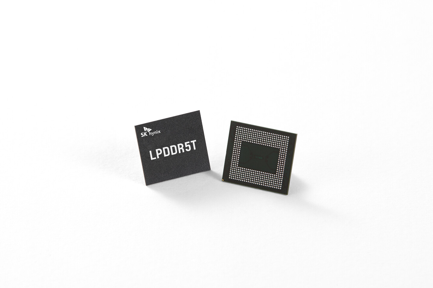
SK Hynix's LPDDR5T, World's Fastest Mobile DRAM, Completes Compatibility Validation with Qualcomm

SK hynix Inc. announced today that it has started commercialization of the LPDDR5T (Low Power Double Data Rate 5 Turbo), the world's fastest DRAM for mobile with 9.6 Gbps speed. The company said that it has obtained the validation that the LPDDR5T is compatible with Qualcomm Technologies' new Snapdragon 8 Gen 3 Mobile Platform, marking the industry's first case for such product to be verified by the U.S. company.

SK hynix has proceeded with the compatibility validation of the LPDDR5T, following the completion of the development in January, with support from Qualcomm Technologies. The completion of the process means that it is compatible with Snapdragon 8 Gen 3. With the validation process with Qualcomm Technologies, a leader in wireless telecommunication products and services, and other major mobile AP (Application Processor) providers successfully completed, SK hynix expects the range of the LPDDR5T adoption to grow rapidly.

SK hynix Starts Mass Production of Industry's First 24GB LPDDR5X DRAM

SK hynix Inc. (or "the company", www.skhynix.com) announced today that it has begun supplying the industry's first 24-gigabyte (GB) Low Power Double Data Rate 5X (LPDDR5X) mobile DRAM package to its customers, following the mass production of LPDDR5X in November 2022. SK hynix, in January, developed LPDDR5T, which is an upgraded product of LPDDR5X prior to the development of the 8th generation LPDDR6, and is currently processing customer validation.

"The company integrated the High-K Metal Gate (HKMG) process in the 24 GB LPDDR5X package, enabling the product to deliver outstanding power efficiency and performance," said SK hynix. "The addition of the 24 GB package to our mobile DRAM product portfolio has given us a more flexibility in accommodating customers' needs."

SK hynix Develops LPDDR5T, World's Fastest Mobile DRAM

SK hynix Inc. announced today that it has developed the world's fastest mobile DRAM 'LPDDR5T (Low Power Double Data Rate 5 Turbo)' and provided sample products to customers. The new product, LPDDR5T, operates at a data rate of 9.6 gigabits per second (Gbps), 13% faster than the previous generation LPDDR5X unveiled in November 2022. To highlight the maximum speed the product features, SK hynix added 'Turbo' at the end of the standard name LPDDR5.

LPDDR5T, which operates in the ultra-low voltage range of 1.01 to 1.12 V set by the JEDEC (Joint Electron Device Engineering Council), is a product that not only features utmost speed but ultra-low power consumption. "The company pushed the technology to new limits in just two months after LPDDR5X, mobile DRAM with 8.5 Gbps specification, was introduced to the market in November 2022," SK hynix said. "We will solidify our leadership in the mobile DRAM market by providing products of various storage capacities that meet customers' needs."

TSMC (Not Intel) Makes the Vast Majority of Logic Tiles on Intel "Meteor Lake" MCM

Intel's next-generation "Meteor Lake" processor is the first mass-production client processor to embody the company's IDM 2.0 manufacturing strategy—one of building processors with multiple logic tiles interconnected with Foveros and a base-tile (essentially an interposer). Each tile is built on a silicon fabrication process most suitable to it, so that the most advanced node could be reserved for the component that benefits from it the most. For example, while you need the SIMD components of the iGPU to be built on an advanced low-power node, you don't need its display controller and media engine to, and these could be relegated to a tile built on a less advanced node. This way Intel is able to maximize its use of wafers for the most advanced nodes in a graded fashion.

Japanese tech publication PC Watch has annotated the "Meteor Lake" SoC, and points out that the vast majority of the chip's tiles and logic die-area is manufactured on TSMC nodes. The MCM consists of four logic tiles—the CPU tile, the Graphics tile, the SoC tile, and the I/O tile. The four sit on a base tile that facilitates extreme-density microscopic wiring interconnecting the logic tiles. The base tile is built on the 22 nm HKMG silicon fabrication node. This tile lacks any logic, and only serves to interconnect the tiles. Intel has an active 22 nm node, and decided it has the right density for the job.

Samsung Launches Industry's First 24Gbps GDDR6 Memory

Samsung Electronics Co., Ltd., the world leader in advanced memory technology, today announced that it has begun sampling the industry's first 16-gigabit (Gb) Graphics Double Data Rate 6 (GDDR6) DRAM featuring 24-gigabit-per-second (Gbps) processing speeds. Built on Samsung's third-generation 10-nanometer-class (1z) process using extreme ultraviolet (EUV) technology, the new memory is designed to significantly advance the graphics performance for next-generation graphics cards (Video Graphics Arrays), laptops and game consoles, as well as artificial intelligence-based applications and high-performance computing (HPC) systems.

"The explosion of data now being driven by AI and the metaverse is pushing the need for greater graphics capabilities that can process massive data sets simultaneously, at extremely high speeds," said Daniel Lee, executive vice president of the Memory Product Planning Team at Samsung Electronics. "With our industry-first 24 Gbps GDDR6 now sampling, we look forward to validating the graphics DRAM on next-generation GPU platforms to bring it to market in time to meet an onslaught of new demand."

Samsung Develops Industry's First HKMG-Based DDR5 Memory; Ideal for Bandwidth-Intensive Advanced Computing Applications

Samsung Electronics Co., Ltd., the world leader in advanced memory technology, today announced that it has expanded its DDR5 DRAM memory portfolio with the industry's first 512 GB DDR5 module based on High-K Metal Gate (HKMG) process technology. Delivering more than twice the performance of DDR4 at up to 7,200 megabits per second (Mbps), the new DDR5 will be capable of orchestrating the most extreme compute-hungry, high-bandwidth workloads in supercomputing, artificial intelligence (AI) and machine learning (ML), as well as data analytics applications.

"Samsung is the only semiconductor company with logic and memory capabilities and the expertise to incorporate HKMG cutting-edge logic technology into memory product development," said Young-Soo Sohn, Vice President of the DRAM Memory Planning/Enabling Group at Samsung Electronics. "By bringing this type of process innovation to DRAM manufacturing, we are able to offer our customers high-performance, yet energy-efficient memory solutions to power the computers needed for medical research, financial markets, autonomous driving, smart cities and beyond."

Intel Launches B365 Express Chipset on 22nm Process, Possibly a Re-branded Z170

Intel today introduced the B365 Express desktop motherboard chipset as an in-between to its B360 Express and H370 Express chipsets. This model is part of Intel's optical enlargement of its motherboard chipsets to the 22 nm HKMG+ silicon fabrication node, to free up 14 nm++ for processors. Despite this, the TDP of the chipset remains unchanged at 6 Watts. The B365 has a couple of feature additions and subtractions over B360. To begin with it has a wider PCI-Express downstream root-complex, with 20 gen 3.0 lanes, on par with H370 Express. The B360, if you'll recall, only has 12 downstream PCIe lanes. This means B365 motherboards will have additional M.2 and U.2 connectivity.

According to the ARK specifications page for the B365 Express, this chip completely lacks integrated 10 Gbps USB 3.1 gen 2 connectivity. Perhaps the expanded downstream PCIe is really meant for motherboard vendors to use third-party USB 3.1 gen 2 controller chips. You still get eight 5 Gbps USB 3.0 ports (notice we didn't say USB 3.1 gen 1, because don't expect fast-charging features). The chipset also loses the latest generation Wireless AC integrated MAC. All of these point to the possibility of the B365 Express being a re-branded Z170 with locked CPU overclocking. Adding credence to this theory is the fact that while the B360 uses ME version 12, the B365 uses the older ME version 11. Much like the H310C, the B365 could include platform support for Windows 7.

Toshiba to Collaborate with GLOBALFOUNDRIES on FFSA Manufacturing

Toshiba Corporation today announced that the company will collaborate with GLOBALFOUNDRIES in the manufacture of Toshiba's FFSA (Fit Fast Structured Array) products. Toshiba will expand its FFSA business through production at GLOBALFOUNDRIES's fabs. Initial products will be manufactured using GLOBALFOUNDRIES 65nm-LPe and 40nm-LP processes, with plans to extend the collaboration to the company's 28nm High-K Metal Gate (HKMG) technology.

Toshiba's FFSA products, developed in collaboration with BaySand Inc. of the U.S., can be configured simply by customizing the design of a few metal layers. This customization process secures a much shorter development turn-around-time than with conventional ASIC devices, and satisfies increasing market needs for high performance, high specifications and low power technologies. At a time of ever-shorter product life cycles, time available for development is at a premium, and solutions that meet demand and allow tweaking of the specifications until just before the start of trial production increase the freedom and flexibility of developers.

RockChip Builds SoCs on GlobalFoundries' 28 nm HKMG Process

GLOBALFOUNDRIES and Fuzhou Rockchip Electronics Co., Ltd. today announced that Rockchip's next-generation mobile processors are ramping to production on GLOBALFOUNDRIES' 28 nm High-K Metal Gate (HKMG) process technology. Based on a multi-core ARM Cortex-A9 design, the RK3188 and RK3168 chips are optimized for tomorrow's high-performance, low-cost tablets that require long-lasting battery life (see product specifications in annex).

The combination of Rockchip's design and GLOBALFOUNDRIES' 28 nm HKMG process technology resulted in a mainstream tablet System-on-Chip (SoC) capable of operating at up to 1.8 GHz performance, while still maintaining the power efficiency expected by mobile device users. The chips began sampling to OEMs in early 2013 and are now ramping to support a wide range of manufacturers.

AMD "Jaguar" Micro-architecture Takes the Fight to Atom with AVX, SSE4, Quad-Core

AMD hedged its low-power CPU bets on the "Bobcat" micro-architecture for the past two years now. Intel's Atom line of low-power chips caught up in power-efficiency, CPU performance, to an extant iGPU performance, and recent models even feature out-of-order execution. AMD unveiled its next-generation "Jaguar" low-power CPU micro-architecture for APUs in the 5W - 25W TDP range, targeting everything from tablets to entry-level notebooks, and nettops.

At its presentation at the 60th ISSC 2013 conference, AMD detailed "Jaguar," revealing a few killer features that could restore the company's competitiveness in the low-power CPU segment. To begin with, APUs with CPU cores based on this micro-architecture will be built on TSMC's 28-nanometer HKMG process. Jaguar allows for up to four x86-64 cores. The four cores, unlike Bulldozer modules, are completely independent, and only share a 2 MB L2 cache.

AMD Announces 2012 FX "Vishera" Line of Performance Desktop Processors

AMD announced the 2012 FX "Vishera" line of eight-core, six-core, and quad-core desktop processors. Based on the new "Piledriver" CPU micro-architecture, the new processors feature increased performance and an updated instruction set, over the previous generation. To begin with, the processors are based around the "Vishera" silicon, built on the 32 nm HKMG process at Global Foundries. With a transistor count of 1.2 billion and a die area of 315 mm², Vishera packs four Piledriver modules, with two cores each, 2 MB L2 cache per module (8 MB total), and 8 MB of L3 cache. Eight-, six-, and four-core models are carved out by toggling the number of modules between four, three, and two.

The Vishera silicon also features an updated CPU instruction set, which includes SSE/2/3/S3/4.1/4.2/4A, AVX, AES-NI, FMA/FMA2/FMA3, XOP, and F16C. An x86 processor by design, Vishera features the AMD64 x86-64 instruction set. Its updated integrated memory controller supports up to 64 GB of dual-channel DDR3 memory, with a standard speed of DDR3-1866 MHz, and more possible with overclocking. The memory interface is single, monolithic 128-bit, unlike the dual 64-bit IMC approach of the "Stars" micro-architecture. Built in the same socket AM3+ package as the previous generation FX, the new chips are compatible with existing AM3+ motherboards with a BIOS update. The 2012 FX processor lineup includes a total of four models, the FX-8350 flagship eight-core, FX-8320 performance eight-core, FX-6300 mainstream six-core, and FX-4300 value quad-core. All models feature unlocked base-clock multipliers, making each of them fit for overclocking. Their specifications and target SEP pricing are tabled below. Market prices could be about 5~10% above the SEP prices.

Samsung and STMicroelectronics Enter Strategic Relationship for 32 nm and 28 nm Tech

Samsung Electronics, Co., Ltd., a world leader in advanced semiconductor technology solutions, announced foundry production of STMicroelectronics' leading products using 32/28nm High-K Metal Gate (HKMG) process technology. Samsung Electronics' foundry business has been selected by STMicroelectronics to provide it with products at the 32/28nm process node. The relationship has already resulted in taping-out of a dozen ST advanced system-on-chip (SoC) devices for mobile, consumer and network applications.

"We have successfully started production of STMicroelectronics' new-generation 32/28nm SoC products," said Kwang-Hyun Kim, executive vice president of Foundry business, Device Solutions, Samsung Electronics. "A foundry relationship with ST demonstrates our commitment to advanced process technology and our 32/28nm HKMG process-technology leadership. We have aggressively ramped 32/28nm capacity and will continue to deliver the most advanced process solutions to our customers."

AMD A-Series "Trinity" Desktop APUs Set for October 1 Launch

According to an OCWorkbench report, AMD will officially launch its second generation A-series desktop APUs on the very first day of Q4 2012, October 1. The launch will include a contingent of socket FM2 motherboards from various manufacturers, based on AMD A55, A75, and A85X chipsets. Among the A-series socket FM2 models launched on October 1, are A10-5800K, A10-5700, A8-5600K, A8-5500, Athlon X4 750K/740, A6-5400K and A4-5300. Built on the 32 nm HKMG process by Globalfoundries, AMD A-series "Trinity" APUs combine up to four x86-64 CPU cores based on the "Piledriver" micro-architecture, with a Radeon HD 7000 series GPU core, with up to 384 stream processors based on the VLIW4 architecture.

GLOBALFOUNDRIES Silicon Validates 28nm AMS Production Design

At next week's Design Automation Conference (DAC) in San Francisco, Calif., GLOBALFOUNDRIES plans to demonstrate an enhanced silicon-validated design flow for its 28nm Super Low Power (SLP) technology with Gate First High-k Metal Gate (HKMG). The flow provides proven and complete front-to-back support for advanced analog/mixed-signal (AMS) design using the industry's latest design automation technology. In addition, the company will reveal jointly developed design flows with its EDA partners in certifying both analog and digital "double patterning aware" flows for its 20nm process, with silicon validation expected in early 2013 at that technology node.

As a result of GLOBALFOUNDRIES' commitment to silicon validation of flows before releasing them, customers have the confidence to produce signoff-ready 28nm digital and analog designs using the industry's most advanced set of design tools, tool scripts, and methodologies from the leading EDA suppliers. The company's tight collaboration with the design tool and IP ecosystem also accelerates its ability to develop working flows for advanced nodes such as 20nm, providing their advantages in gate density, performance, and lower power to customers ahead of other foundries.

GLOBALFOUNDRIES Improves IC Reliability with Customized Circuit Checks

Mentor Graphics Corp. today announced that GLOBALFOUNDRIES is helping its customers improve reliability checking by adding Calibre PERC to select 28nm bulk CMOS design enablement flows. Calibre PERC will give designers access to the new reliability verification rules developed by the IBM Semiconductor Development Alliance (ISDA), augmented with GLOBALFOUNDRIES specific checks to help prevent external latch-up. Using Calibre PERC's unique architecture, complex reliability rules that require the integration of logical (net list) and layout (GDS) information can be fully automated, eliminating manual spreadsheet-based efforts and reducing the chances of design errors.

"In the past, verification of latch-up immunity depended on manual layout checks and rough approximations of device and interconnect resistance using traditional mechanisms," said Bill Liu, vice president of design enablement at GLOBALFOUNDRIES. "Now our customers can perform accurate measurements and analysis automatically using Calibre PERC's data integration capability. For example, some of our customers are currently using PERC to accurately determine the resistance of the paths in complex output driver arrays as a function of device spacing. This allows them to easily and accurately detect points in the circuit where latch-up could be an issue and to make appropriate improvements."

NVIDIA Credits Close Collaboration with TSMC for Kepler's Energy Efficiency

Despite the fact that NVIDIA is frantically seeking out other semiconductor foundries for high-volume manufacturing its 28 nm chip designs, and despite some looming irritants, NVIDIA appears to value its relationship with TSMC highly. NVIDIA's senior vice president for Advanced Technology Group Joe Greco, in a recent company blog post, credited close collaboration with TSMC for the stellar energy-efficiency (performance/Watt) figures NVIDIA's Kepler architecture has been able to achieve.

"The advancement that TSMC offered was a new optimized process technology. Kepler is manufactured using TSMC's 28nm high performance (HP) process, the foundry's most advanced 28nm process which uses their first-generation high-K metal gate (HKMG) technology and second generation SiGe (Silicon Germanium) straining," read the blog post. "Using TSMC's 28nm HP process enabled us to reduce active power by about 15 percent and leakage by about 50 percent compared to 40nm, resulting in an overall improvement in power efficiency of about 35 percent (see charts)."

Samsung’s New Quad-Core Application Processor Drives Advanced Feature Sets

Samsung Electronics Co. Ltd., a world leader in advanced semiconductor solutions, today introduced the industry's first quad-core application processor built on the High-k Metal Gate (HKMG) low-power process technology. With unprecedented performance capabilities exceeding 1.4GHz based on the ARM CORTEX A9 quad-core, the powerful, yet energy-efficient Exynos 4 Quad, allows system-level architects to integrate maximized power efficiencies into smartphones and tablets which enables double the processing power at a 20 percent lower power bill over its predecessor, the 45nm process-based Exynos 4 Dual.

"The quad-core processor offers phenomenal multitasking abilities surpassing any single or dual application processor. Since all the cores must share a single battery, the power management and efficiency in the limited battery capacity are indispensable for mobile computing devices," said Taehoon Kim, vice president of System LSI marketing, Device Solutions, Samsung Electronics. "Given the diverse functionalities consumers are demanding from their mobile devices today, the Exynos 4 Quad meets those high-performance needs while keeping power consumption very low."

GLOBALFOUNDRIES Dresden Fab Ships 250,000th 32 nm HKMG Wafer

GLOBALFOUNDRIES today announced that its Fab 1 in Dresden, Germany has shipped a quarter of a million semiconductor wafers based on 32nm High-k Metal Gate (HKMG) technology. The milestone represents a significant lead over other foundries in HKMG manufacturing and carries on a long tradition of rapidly ramping leading-edge technologies to volume production.

On a unit basis, cumulative 32nm shipments for the first five quarters of wafer production are more than double that achieved during the same period of the 45nm technology ramp, demonstrating that the overall 32nm ramp has significantly outpaced the 45nm ramp, despite the integration of a number of new and complex elements in both design and process technologies.

First 28 nm Cortex-A9 POP Available for GLOBALFOUNDRIES 28nm-SLP HKMG Process

ARM today announced the availability of the ARM Cortex-A9 MPCore Processor Optimization Pack (POP) for GLOBALFOUNDRIES' 28 nm-SLP High-K Metal Gate process technology. Optimized for mobile, networking and enterprise applications, the energy-efficient ARM POP 28 nm-SLP for Cortex-A9 processors delivers a performance range from 1 GHz to 1.6 GHz for worst case conditions, with up to 2 GHz in typical conditions. This provides a wide range of flexibility for System-on-Chip (SoC) designers to optimize performance and energy-efficiency using the ARM Artisan Physical IP Platform and Cortex-A9 POP.

GLOBALFOUNDRIES and ARM Deliver Optimized SoC Solution based on ARM Cortex-A Series

GLOBALFOUNDRIES and ARM today revealed the latest advances in their longstanding collaboration to deliver optimized system-on-chip (SoC) solutions for ARM Cortex-A series processor designs using ARM Artisan advanced physical IP and GLOBALFOUNDRIES' leading-edge process technologies. The companies announced the industry's first test chip based on a dual-core Cortex-A9 processor operating at frequencies of more than 2.5GHz. In addition, a 20nm tape out using GLOBALFOUNDRIES' Technology Qualification Vehicle (TQV) was also announced for SoCs based on Cortex-A9 processors.

The two companies worked closely together to develop a TQV strategy that allows GLOBALFOUNDRIES to optimize its advanced process technology for customer designs based on Cortex-A series processors. The solution is more than a standard test chip. Each TQV is designed to emulate a full specification SoC and aims to improve performance, lower power consumption and facilitate a faster path to market for foundry customers.

AMD to Turn to TSMC for ''Bulldozer'' Manufacturing

AMD is rumored to be seeking ties with TSMC, Taiwan's premier semiconductor manufacturing foundry, for future manufacturing of its "Bulldozer" architecture processors, according to a report by DonanimHaber. This has two very distinct implications: first, AMD could be facing issues with GlobalFoundries 32 nm HKMG node, its de facto foundry for CPU manufacturing, and second, this could just be an obvious development of future low-power APUs based on the new x86 architecture being manufactured at TSMC, much like how current E-series and C-series APUs are.

Then again, AMD doesn't exactly have any APUs in works that use "Bulldozer" architecture for the x86 cores, rather, its successor codenamed "Piledriver". Another couple of important things to note here are that TSMC does not have a 32 nm bulk node (it was scrapped with the transition to 28 nm bulk), and its HKMG (high-K metal gate transistor) manufacturing technology is deployed rather recently. It would be interesting to follow this development.

AMD Trinity A-Series APUs to Pack Radeon 7000 Series Graphics

An internal presentation slide leaked to the press reveals some details of AMD's next generation "Trinity" APUs that succeed current generation A-Series "Llano" Fusion series. The presentation was run by AMD's principal foundry partner, Global Foundries, outlining upcoming products built on the 32 nm High-K metal gate transistor (HKMG) process. With Trinity, AMD is expecting a 50% improvement in gigaFLOP performance over the present generation, which doesn't sound far-fetched considering it will use next-generation Piledriver CPU core architecture and Radeon HD 7000 series graphics, which uses VLIW4 stream processor architecture.

Piledriver is an evolved x86 architecture that uses the modular shared resource design of Bulldozer, with much higher IPC compared to Stars architecture. VLIW4 stream processors ensure higher performance per square millimeter die area. Trinity will be available for notebooks as "Comal" and "Virgo" for desktops. They will be branded in the A-Series. AMD expects a 2012 market entry for the two.

AMD Introduces Vision A6-3650 and A8-3850 Desktop APUs

AMD announced two of its first Vision A-Series accelerated processing units (APUs) for desktops today. Built in the socket FM1 package, the A6-3650 and A8-3850 are fabricated on the 32 nm HKMG process. Both pack four x86-64 cores, and while the A6 has 320 stream processors in the GPU component, the A8 has 400 of them. Both chips have 4 MB of cache, dual-channel DDR3-1866 MHz IMCs, and PCI-Express 2.0 hubs to drive discrete graphics.

The AMD A8-3850 has its four x86-64 cores clocked at 2.90 GHz, with the Radeon HD 6550D GPU engine clocked at 600 MHz. This chip has a TDP of 100W, it is priced at US $135. The AMD A6-3650 has its CPU component clocked at 2.60 GHz, and Radeon HD 6530D GPU engine clocked at 443 MHz. This chip goes for US $115. With these two, AMD is targeting higher models of Sandy Bridge-based Pentium Dual-Core and Core i3 Sandy Bridge chips. Both will be available in stores by July 3.

Elpida Uses High-k Metal Gate Technology to Develop 2-gigabit DDR2 Mobile RAM

Elpida Memory, Inc., Japan's leading global supplier of Dynamic Random Access Memory (DRAM), today announced the DRAM industry's first-ever use of high-k metal gate (HKMG) technology to develop a 2-gigabit DDR2 Mobile RAM (LPDDR2) at the 40nm-class DRAM node.

HKMG is technology that uses insulator film with a high dielectric constant (abbreviated to "high-k," a semiconductor industry measure of how much charge a material can hold) in the transistor gate to reduce current leakage and improve transistor performance. Metal gate electrodes that are required for the high-k dielectrics process are also used. Some makers of logic semiconductors have started to use HKMG, but higher heat treatment temperatures after HKMG formation and complicated DRAM structural characteristics have prevented consistent application in the DRAM fabrication process. Elpida, however, has managed to lower the heat treatment load and overcome certain memory device structural complications.

Intel Reveals New Logos and a Die Shot of Second Generation Core Processors

At the keynote of Intel Developer Forum 2010, the silicon giant gave a sneak-peak into its upcoming processor brand, revealing new product logos (case badges), and a die-shot of the Sandy Bridge quad-core silicon. Intel retains the Core i3, Core i5, and Core i7 brand identifiers, but refers to the family of processors based on the Sandy Bridge architecture as second-generation Core processors or the 2011 Intel Core processors. For the same reason, processor model numbers start with the 2000 series as detailed in this article.

The die shot reveals integration of the IGP-embedded northbridge component completely into the processor die. In "Clarkdale" Core i3 and Core i5 processors, the northbridge component was present on a separate die from the CPU die, with a QPI link connecting the two dies on the same package. The Sandy Bridge quad-core die is known to feature 6 MB of L3 cache, a dual-channel DDR3 IMC, and a DirectX 10.1 compliant graphics processor. Apart from merely driving graphics, the IGP also feature several media-acceleration features that speed up video encoding. Sandy Bridge is fabricated on the 32 nanometer HKMG process. The evolution of Intel's architectures is shown on the last picture. The "Nehalem" chip there is the Lynnfield quad-core processor that completely lacks an IGP, "Westmere" is the Clarkdale dual-core processor that has an IGP and memory controller on a second (larger) 45 nm die. The chip to the right is a 32 nm Sandy Bridge that integrates a quad-core chip with an IGP-embedded northbridge.
Return to Keyword Browsing
May 2nd, 2024 21:15 EDT change timezone

New Forum Posts

Popular Reviews

Controversial News Posts