News Posts matching #HPC

Return to Keyword Browsing

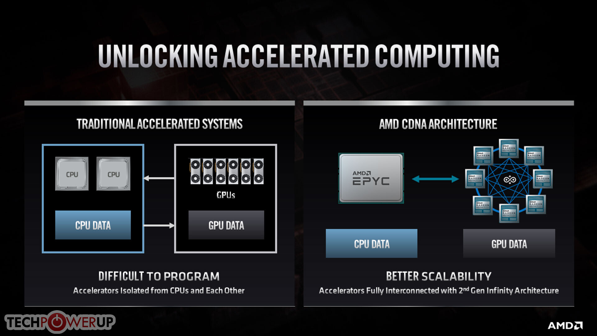
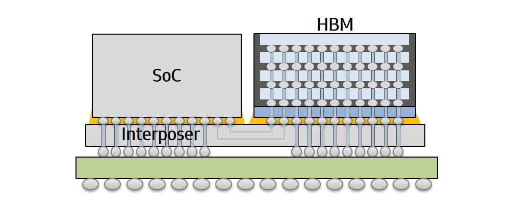
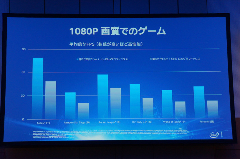
Micron to Launch HBM2 Memory This Year

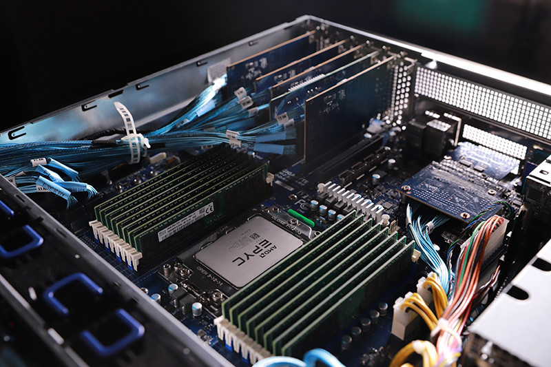
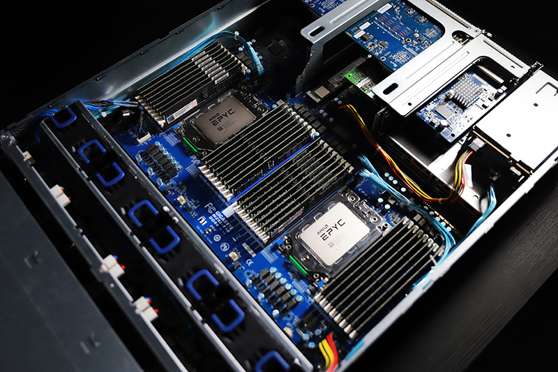
Micron Technologies, in the latest earnings report, announced that they will start shipping High-Bandwidth Memory 2 (HBM2) DRAM. Used for high-performance graphics cards, server processors and all kinds of processors, HBM2 memory is wanted and relatively expensive solution, however, when Micron enters the market of its manufacturing, prices, and the market should adjust for the new player. Previously, only SK-Hynix and Samsung were manufacturing the HBM2 DRAM, however, Micron will join them and they will again form a "big-three" pact that dominates the memory market.

Up until now, Micron used to lay all hopes on its proprietary Hybrid Memory Cube (HMC) DRAM type, which didn't gain much traction from customers and it never really took off. Only a few rare products used it, as Fujitsu SPARC64 XIfx CPU used in Fujitsu PRIMEHPC FX100 supercomputer introduced in 2015. Micron announced to suspend works on HMC in 2018 and decided to devote their efforts to GDDR6 and HBM development. So, as a result, we are seeing that they will launch HBM2 DRAM products sometime this year.
Micron HMC High-Bandwidth Memory

Intel Scales Neuromorphic Research System to 100 Million Neurons

Today, Intel announced the readiness of Pohoiki Springs, its latest and most powerful neuromorphic research system providing the computational capacity of 100 million neurons. The cloud-based system will be made available to members of the Intel Neuromorphic Research Community (INRC), extending their neuromorphic work to solve larger, more complex problems.

"Pohoiki Springs scales up our Loihi neuromorphic research chip by more than 750 times, while operating at a power level of under 500 watts. The system enables our research partners to explore ways to accelerate workloads that run slowly today on conventional architectures, including high-performance computing (HPC) systems." -Mike Davies, director of Intel's Neuromorphic Computing Lab.
Intel Pohoiki Springs Intel Pohoiki Springs Intel Pohoiki Springs Intel Pohoiki Springs

AMD Announces the CDNA and CDNA2 Compute GPU Architectures

AMD at its 2020 Financial Analyst Day event unveiled its upcoming CDNA GPU-based compute accelerator architecture. CDNA will complement the company's graphics-oriented RDNA architecture. While RDNA powers the company's Radeon Pro and Radeon RX client- and enterprise graphics products, CDNA will power compute accelerators such as Radeon Instinct, etc. AMD is having to fork its graphics IP to RDNA and CDNA due to what it described as market-based product differentiation.

Data centers and HPCs using Radeon Instinct accelerators have no use for the GPU's actual graphics rendering capabilities. And so, at a silicon level, AMD is removing the raster graphics hardware, the display and multimedia engines, and other associated components that otherwise take up significant amounts of die area. In their place, AMD is adding fixed-function tensor compute hardware, similar to the tensor cores on certain NVIDIA GPUs.
AMD Datacenter GPU Roadmap CDNA CDNA2 AMD CDNA Architecture AMD Exascale Supercomputer

AMD Financial Analyst Day 2020 Live Blog

AMD Financial Analyst Day presents an opportunity for AMD to talk straight with the finance industry about the company's current financial health, and a taste of what's to come. Guidance and product teasers made during this time are usually very accurate due to the nature of the audience. In this live blog, we will post information from the Financial Analyst Day 2020 as it unfolds.
20:59 UTC: The event has started as of 1 PM PST. CEO Dr Lisa Su takes stage.

Kingston Releases DC1000M U.2 NVMe SSDs for Mixed-use in Data Centers

Kingston Digital, Inc., the Flash memory affiliate of Kingston Technology Company, Inc., a world leader in memory products and technology solutions, today announced the availability of DC1000M, a new U.2 data center NVMe PCIe SSD. DC1000M is designed to support a wide range of data-intensive enterprise workloads, including Cloud computing, web hosting, high-performance computing (HPC), virtual infrastructures, artificial intelligence and deep learning applications. DC1000M joins the recently released DC1000B NVMe boot drive, the VMware Ready DC500 series SATA SSDs and DC450R to form the most complete range of superior enterprise-class data center storage solutions in the market.

"Mission critical services and Cloud-based applications depend not only on lightning-fast IOPS and bandwidth, but also on the consistency and predictability of the data being serviced," said Keith Schimmenti, enterprise SSD business manager, Kingston. "DC1000M provides the stability and low latency for the evolving data center, while powering the workloads that require one drive write per day (1 DWPD) endurance."

Ampere Computing Uncovers 80 Core "Cloud-Native" Arm Processor

Ampere Computing, a startup focusing on making HPC and processors from cloud applications based on Arm Instruction Set Architecture, today announced the release of a first 80 core "cloud-native" processor based on the Arm ISA. The new Ampere Altra CPU is the company's first 80 core CPU meant for hyper scalers like Amazon AWS, Microsoft Azure, and Google Cloud. Being built on TSMC's 7 nm semiconductor manufacturing process, the Altra is a CPU that is utilizing a monolithic die to achieve maximum performance. Using Arm's v8.2+ instruction set, the CPU is using the Neoverse N1 platform as its core, to be ready for any data center workload needed. It also borrows a few security features from v8.3 and v8.5, namely the hardware mitigations of speculative attacks.

When it comes to the core itself, the CPU is running at 3.0 GHz frequency and has some very interesting specifications. The design of the core is such that it is 4-wide superscalar Out of Order Execution (OoOE), which Ampere refers to as "aggressive" meaning that there is a lot of data throughput going on. The cache levels are structured in a way that there is 64 KB of L1D and L1I cache per core, along with 1 MB of L2 cache per core as well. For system-level cache, there is 32 MB of L3 available to the SoC. All of the caches have Error-correcting code (ECC) built-in, giving the CPU a much-needed feature. There are two 128-bit wide Single Instruction Multiple Data (SIMD) units, which are there to do parallel processing if needed. There is no mention if they implement Arm's Scalable Vector Extensions (SVE) or not.

TSMC to Hire 4000 new Staff for Next-Generation Semiconductor Node Development

TSMC is set to hire about 4000 new staff members to gain a workforce for its development of next-generation semiconductor manufacturing nodes. The goal of the company is to gather talent so it can develop the world's leading semiconductor nodes, like 3 nm and below. With 15 billion USD planned for R&D purposes alone this year, TSMC is investing a big part of its capital back into development on new and improved technology. Markets such as 5G and High-Performance Computing are leading the charge and require smaller, faster, and more efficient semiconductor nodes, which TSMC plans to deliver. To gather talent, TSMC started job listing using recruitment website TaiwanJobs and started campaigns on university campuses to attract grad students.

ASUS Announces Exclusive Power Balancer Technology and Servers with New 2nd Gen Intel Xeon Scalable

ASUS, the leading IT Company in server systems, server motherboards, workstations and workstation motherboards today announced exclusive Power Balancer technology to support the new 2nd Gen Intel Xeon Scalable Processor (extended Cascade Lake-SP refresh SKUs) across all server product lineups, including the RS720/720Q/700 E9, RS520/500 E9 and ESC8000/4000 G4 series server systems and Z11 server motherboards.

In complex applications, such as high-performance computing (HPC), AI or edge computing, balancing performance and power consumption is always a challenge. With Power Balancer technology and the new 2nd Gen Intel Xeon Scalable Processor, ASUS servers save up to 31 watts power per node on specific workloads and achieve even better efficiency with more servers in large-scale environments, significantly decreasing overall power consumption for a much lower total cost of ownership and optimized operations.

Samsung Launches 3rd-Generation "Flashbolt" HBM2E Memory

Samsung Electronics, the world leader in advanced memory technology, today announced the market launch of 'Flashbolt', its third-generation High Bandwidth Memory 2E (HBM2E). The new 16-gigabyte (GB) HBM2E is uniquely suited to maximize high performance computing (HPC) systems and help system manufacturers to advance their supercomputers, AI-driven data analytics and state-of-the-art graphics systems in a timely manner.

"With the introduction of the highest performing DRAM available today, we are taking a critical step to enhance our role as the leading innovator in the fast-growing premium memory market," said Cheol Choi, executive vice president of Memory Sales & Marketing at Samsung Electronics. "Samsung will continue to deliver on its commitment to bring truly differentiated solutions as we reinforce our edge in the global memory marketplace."

Europe Readies its First Prototype of Custom HPC Processor

European Processor Initiative (EPI) is a Europe's project to kickstart a homegrown development of custom processors tailored towards different usage models that the European Union might need. The first task of EPI is to create a custom processor for high-performance computing applications like machine learning, and the chip prototypes are already on their way. The EPI chairman of the board Jean-Marc Denis recently spoke to the Next Platform and confirmed some information regarding the processor design goals and the timeframe of launch.

Supposed to be manufactured on TSMC's 6 nm EUV (TSMC N6 EUV) technology, the EPI processor will tape-out at the end of 2020 or the beginning of 2021, and it is going to be heterogeneous. That means that on its 2.5D die, many different IPs will be present. The processor will use a custom ARM CPU, based on a "Zeus" iteration of Neoverese server core, meant for general-purpose computation tasks like running the OS. When it comes to the special-purpose chips, EPI will incorporate a chip named Titan - a RISC-V based processor that uses vector and tensor processing units to compute AI tasks. The Titan will use every new standard for AI processing, including FP32, FP64, INT8, and bfloat16. The system will use HBM memory allocated to the Titan processor, have DDR5 links for the CPU, and feature PCIe 5.0 for the inner connection.

Intel Unveils Xe DG1-SDV Graphics Card, Demonstrates Intent to Seriously Compete in the Gaming Space

At a media event on Wednesday, Intel invited us to check out their first working modern discrete graphics card, the Xe DG1 Software Development Vehicle (developer-edition). Leading the event was our host Ari Rauch, Intel Vice President and General Manager for Graphics Technology Engineering and dGPU Business. Much like gruff developer-editions of game consoles released to developers several quarters ahead of market launch, the DG1-SDV allows software developers to discover and learn the Xe graphics architecture, and develop optimization processes for their current and future software within their organizations. We walked into the event expecting to see a big ugly PCB with a bare fan-heatsink and a contraption that sort-of looks like a graphics card; but were pleasantly surprised with what we saw: a rather professional product design.

What we didn't get at the event, through, was a juicy technical breakdown of the Xe graphics architecture, and its various components that add up to the GPU. We still left pleasantly surprised for what we were shown: it works! The DG1-SDV is able to play games at 1080p, even if they are technically lightweight titles like "Warframe," and aren't maxing out settings. The SDV is a 15.2 cm-long graphics card that relies on the PCI-Express slot for power entirely (and hence pulling less than 75 W).

Samsung Starts Production of AI Chips for Baidu

Baidu, a leading Chinese-language Internet search provider, and Samsung Electronics, a world leader in advanced semiconductor technology, today announced that Baidu's first cloud-to-edge AI accelerator, Baidu KUNLUN, has completed its development and will be mass-produced early next year. Baidu KUNLUN chip is built on the company's advanced XPU, a home-grown neural processor architecture for cloud, edge, and AI, as well as Samsung's 14-nanometer (nm) process technology with its I-Cube (Interposer-Cube) package solution.

The chip offers 512 gigabytes per second (GBps) memory bandwidth and supplies up to 260 Tera operations per second (TOPS) at 150 watts. In addition, the new chip allows Ernie, a pre-training model for natural language processing, to infer three times faster than the conventional GPU/FPGA-accelerating model. Leveraging the chip's limit-pushing computing power and power efficiency, Baidu can effectively support a wide variety of functions including large-scale AI workloads, such as search ranking, speech recognition, image processing, natural language processing, autonomous driving, and deep learning platforms like PaddlePaddle.

Intel Announces New GPU Architecture and oneAPI for Unified Software Stack at SC19

At Supercomputing 2019, Intel unveiled its vision for extending its leadership in the convergence of high-performance computing (HPC) and artificial intelligence (AI) with new additions to its data-centric silicon portfolio and an ambitious new software initiative that represents a paradigm shift from today's single-architecture, single-vendor programming models.

Addressing the increasing use of heterogeneous architectures in high-performance computing, Intel expanded on its existing technology portfolio to move, store and process data more effectively by announcing a new category of discrete general-purpose GPUs optimized for AI and HPC convergence. Intel also launched the oneAPI industry initiative to deliver a unified and simplified programming model for application development across heterogenous processing architectures, including CPUs, GPUs, FPGAs and other accelerators. The launch of oneAPI represents millions of Intel engineering hours in software development and marks a game-changing evolution from today's limiting, proprietary programming approaches to an open standards-based model for cross-architecture developer engagement and innovation.

AMD Reports Third Quarter 2019 Financial Results

AMD (NASDAQ:AMD) today announced revenue for the third quarter of 2019 of $1.80 billion, operating income of $186 million, net income of $120 million and diluted earnings per share of $0.11. On a non-GAAP(*) basis, operating income was $240 million, net income was $219 million and diluted earnings per share was $0.18.

"Our first full quarter of 7 nm Ryzen, Radeon and EPYC processor sales drove our highest quarterly revenue since 2005, our highest quarterly gross margin since 2012 and a significant increase in net income year-over-year," said Dr. Lisa Su, AMD president and CEO. "I am extremely pleased with our progress as we have the strongest product portfolio in our history, significant customer momentum and a leadership product roadmap for 2020 and beyond."

PCI-Express Gen 6.0 Specification to Finalize by 2021

With 64 Gbps bandwidth per lane, 256 Gbps in x4, and a whopping 1 Tbps in x16 (128 GB/s per direction), PCI-Express 6.0 will debut in 2021 as 5G adoption hits critical mass in markets across the globe, to support server nodes, high-bandwidth network infrastructure, and lighting fast I/O for HPC and AI applications. Development of the new standard is already underway, with the specification having achieved a pre-release version 0.3, according to the PCI-SIG, the body that develops and maintains the PCI IP.

Further development, prototyping, and testing of the standard will run through 2020 as drafts of the standard are dispatched to interested parties. With the specification published in 2021, the first devices implementing it could arrive the following year. Granted, very few devices need 1 Tbps bandwidth, but the exercise of doubling bandwidth every 3 or so years has its maximum impact on devices that only have wiring for one PCIe lane, and directly impacts bandwidth of other I/O specifications that are derived from PCIe, such as USB, Thunderbolt, CXL, etc.

Intel Mobility Xe GPUs to Feature Up to Twice the Performance of Previous iGPUs

Intel at the Intel Developer Conference 'IDC' 2019 in Tokyo revealed their performance projections for mobility Xe GPUs, which will supersede their current consumer-bound UHD620 graphics under the Gen 11 architecture. The company is being vocal in that they can achieve an up to 2x performance uplift over their previous generation - but that will likely only take place in specific scenarios, and not as a rule of thumb. Just looking at Intel's own performance comparison graphics goes to show that we're mostly looking at between 50% and 70% performance improvements in popular eSports titles, which are, really, representative of most of the gaming market nowadays.

The objective is to reach above 60 FPS in the most popular eSports titles, something that Gen 11 GPUs didn't manage with their overall IPC and dedicated die-area. We've known for some time that Intel's Xe (as in, exponential) architecture will feature hardware-based raytracing, and the architecture is being developed for scalability that goes all the way from iGPUs to HPC platforms.

Samsung Develops Industry's First 12-Layer 3D-TSV Chip Packaging Technology

Samsung Electronics Co., Ltd., a world leader in advanced semiconductor technology, today announced that it has developed the industry's first 12-layer 3D-TSV (Through Silicon Via) technology. Samsung's new innovation is considered one of the most challenging packaging technologies for mass production of high-performance chips, as it requires pinpoint accuracy to vertically interconnect 12 DRAM chips through a three-dimensional configuration of more than 60,000 TSV holes, each of which is one-twentieth the thickness of a single strand of human hair.

The thickness of the package (720 µm) remains the same as current 8-layer High Bandwidth Memory-2 (HBM2) products, which is a substantial advancement in component design. This will help customers release next-generation, high-capacity products with higher performance capacity without having to change their system configuration designs. In addition, the 3D packaging technology also features a shorter data transmission time between chips than the currently existing wire bonding technology, resulting in significantly faster speed and lower power consumption.

New NetCAT Vulnerability Exploits DDIO on Intel Xeon Processors to Steal Data

DDIO, or Direct Data I/O, is an Intel-exclusive performance enhancement that allows NICs to directly access a processor's L3 cache, completely bypassing the a server's RAM, to increase NIC performance and lower latencies. Cybersecurity researchers from the Vrije Universiteit Amsterdam and ETH Zurich, in a research paper published on Tuesday, have discovered a critical vulnerability with DDIO that allows compromised servers in a network to steal data from every other machine on its local network. This include the ability to obtain keystrokes and other sensitive data flowing through the memory of vulnerable servers. This effect is compounded in data centers that have not just DDIO, but also RDMA (remote direct memory access) enabled, in which a single server can compromise an entire network. RDMA is a key ingredient in shoring up performance in HPCs and supercomputing environments. Intel in its initial response asked customers to disable DDIO and RDMA on machines with access to untrusted networks, while it works on patches.

The NetCAT vulnerability spells big trouble for web hosting providers. If a hacker leases a server in a data-center with RDMA and DDIO enabled, they can compromise other customers' servers and steal their data. "While NetCAT is powerful even with only minimal assumptions, we believe that we have merely scratched the surface of possibilities for network-based cache attacks, and we expect similar attacks based on NetCAT in the future," the paper reads. We hope that our efforts caution processor vendors against exposing microarchitectural elements to peripherals without a thorough security design to prevent abuse." The team also published a video briefing the nature of NetCAT. AMD EPYC processors don't support DDIO.
The video detailing NetCAT follows.

GIGABYTE Smashes 11 World Records with New AMD EPYC 7002 Processors

GIGABYTE, a leading server systems builder which recently released a total of 17 new AMD EPYC 7002 Series "Rome" server platforms simultaneously with AMD's own official launch of their next generation CPU, is proud to announce that our new systems have already broken 11 different SPEC benchmark world records. These new world records have not only been achieved against results from all alternative processor based systems but even against competing vendor solutions using the same 2nd Generation AMD EPYC 7002 Series "Rome" processor platform, illustrating that GIGABYTE's system design and engineering is perfectly optimized to deliver the maximum performance possible from the 2nd Generation AMD EPYC.

2nd Gen AMD EPYC Processors Set New Standard for the Modern Datacenter

At a launch event today, AMD was joined by an expansive ecosystem of datacenter partners and customers to introduce the 2nd Generation AMD EPYC family of processors that deliver performance leadership across a broad number of enterprise, cloud and high-performance computing (HPC) workloads. 2nd Gen AMD EPYC processors feature up to 64 "Zen 2" cores in leading-edge 7 nm process technology to deliver record-setting performance while helping reduce total cost of ownership (TCO) by up to 50% across numerous workloads. At the event, Google and Twitter announced new 2nd Gen AMD EPYC processor deployments and HPE and Lenovo announced immediate availability of new platforms.

"Today, we set a new standard for the modern datacenter with the launch of our 2nd Gen AMD EPYC processors that deliver record-setting performance and significantly lower total cost of ownership across a broad set of workloads," said Dr. Lisa Su, president and CEO, AMD. "Adoption of our new leadership server processors is accelerating with multiple new enterprise, cloud and HPC customers choosing EPYC processors to meet their most demanding server computing needs."

NVIDIA Brings CUDA to ARM, Enabling New Path to Exascale Supercomputing

NVIDIA today announced its support for Arm CPUs, providing the high performance computing industry a new path to build extremely energy-efficient, AI-enabled exascale supercomputers. NVIDIA is making available to the Arm ecosystem its full stack of AI and HPC software - which accelerates more than 600 HPC applications and all AI frameworks - by year's end. The stack includes all NVIDIA CUDA-X AI and HPC libraries, GPU-accelerated AI frameworks and software development tools such as PGI compilers with OpenACC support and profilers. Once stack optimization is complete, NVIDIA will accelerate all major CPU architectures, including x86, POWER and Arm.

"Supercomputers are the essential instruments of scientific discovery, and achieving exascale supercomputing will dramatically expand the frontier of human knowledge," said Jensen Huang, founder and CEO of NVIDIA. "As traditional compute scaling ends, power will limit all supercomputers. The combination of NVIDIA's CUDA-accelerated computing and Arm's energy-efficient CPU architecture will give the HPC community a boost to exascale."

The EPI Announces Successful First Steps Towards a Made-in-Europe High-performance Microprocessor

The European Processor Initiative(EPI), crucial element of the European exascale strategy, delivers its first architectural design to the European Commission and welcomes new partners Almost six months in, the project that kicked off last December has already delivered its first architectural designs to the European Commission, thus marking initial milestones successfully executed. The project that will be the cornerstone of the EU's strategic plans in HPC initially brought together 23 partners from 10 European countries, but has now welcomed three more strong additions to its EPI family. EPI consortium aims to bring a low-power microprocessor to the market and ensure that the key competences for high-end chip design remain in Europe. The European Union's Horizon 2020 program funds this project with a special Framework Partnership Agreement. The initial stage is a three-year Specific Grant Agreement, which lasts until November 2021.

Samsung Successfully Completes 5nm EUV Development

Samsung Electronics Co., Ltd., a world leader in advanced semiconductor technology, today announced that its 5-nanometer (nm) FinFET process technology is complete in its development and is now ready for customers' samples. By adding another cutting-edge node to its extreme ultraviolet (EUV)-based process offerings, Samsung is proving once again its leadership in the advanced foundry market.

Compared to 7 nm, Samsung's 5 nm FinFET process technology provides up to a 25 percent increase in logic area efficiency with 20 percent lower power consumption or 10 percent higher performance as a result of process improvement to enable us to have more innovative standard cell architecture. In addition to power performance area (PPA) improvements from 7 nm to 5 nm, customers can fully leverage Samsung's highly sophisticated EUV technology. Like its predecessor, 5 nm uses EUV lithography in metal layer patterning and reduces mask layers while providing better fidelity.

Intel Announces Broadest Product Portfolio for Moving, Storing, and Processing Data

Intel Tuesday unveiled a new portfolio of data-centric solutions consisting of 2nd-Generation Intel Xeon Scalable processors, Intel Optane DC memory and storage solutions, and software and platform technologies optimized to help its customers extract more value from their data. Intel's latest data center solutions target a wide range of use cases within cloud computing, network infrastructure and intelligent edge applications, and support high-growth workloads, including AI and 5G.

Building on more than 20 years of world-class data center platforms and deep customer collaboration, Intel's data center solutions target server, network, storage, internet of things (IoT) applications and workstations. The portfolio of products advances Intel's data-centric strategy to pursue a massive $300 billion data-driven market opportunity.

Without Silicon, Intel Scores First Exascale Computer Design Win for Xe Graphics - AURORA Supercomputer

This here is an interesting piece of tech news for sure, in that Intel has already scored a pretty massive design win for not one, but two upcoming products. Intel's "Future Xeon Scalable Processors" and the company's "Xe Compute Architecture" have been tapped by the U.S. Department of Energy for incorporation into the new AURORA Supercomputer - one that will deliver exascale performance. AURORA is to be developed in a partnership between Intel and Cray, using the later's Shasta systems and its "Slingshot" networking fabric. But these are not the only Intel elements in the supercomputer design: Intel's DC Optane persistent memory will also be employed (in an as-of-yet-unavailable version of it as well), making this a full win across the prow for Intel.
Return to Keyword Browsing
Jul 1st, 2025 21:34 CDT change timezone

New Forum Posts

Popular Reviews

TPU on YouTube

Controversial News Posts