Thursday, March 5th 2020

AMD Financial Analyst Day 2020 Live Blog
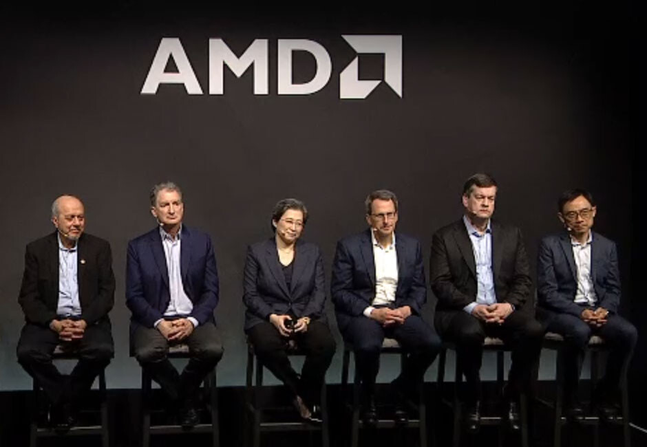
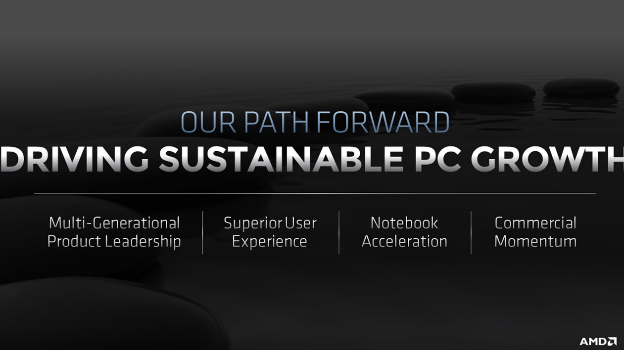
AMD Financial Analyst Day presents an opportunity for AMD to talk straight with the finance industry about the company's current financial health, and a taste of what's to come. Guidance and product teasers made during this time are usually very accurate due to the nature of the audience. In this live blog, we will post information from the Financial Analyst Day 2020 as it unfolds. 20:59 UTC: The event has started as of 1 PM PST. CEO Dr Lisa Su takes stage.


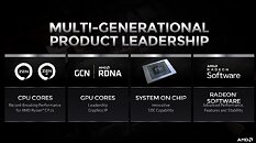
21:05 UTC: AMD details its strategy, that the backbones of its business are "Graphics", "Compute" and "Solutions". 21:07 UTC: High performance computing (including enterprise HPC) is a focus area for AMD.
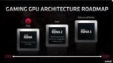
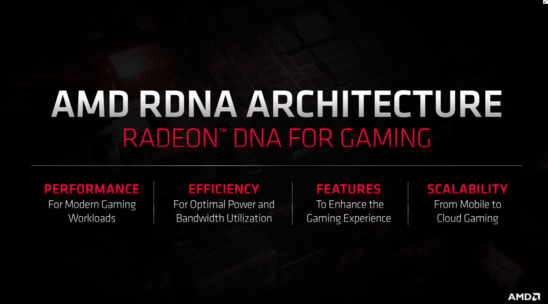
 21:08 UTC: RDNA will last us for the next five years, AMD will continue to invest in their Radeon Graphics RDNA architecture.
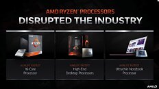
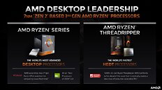
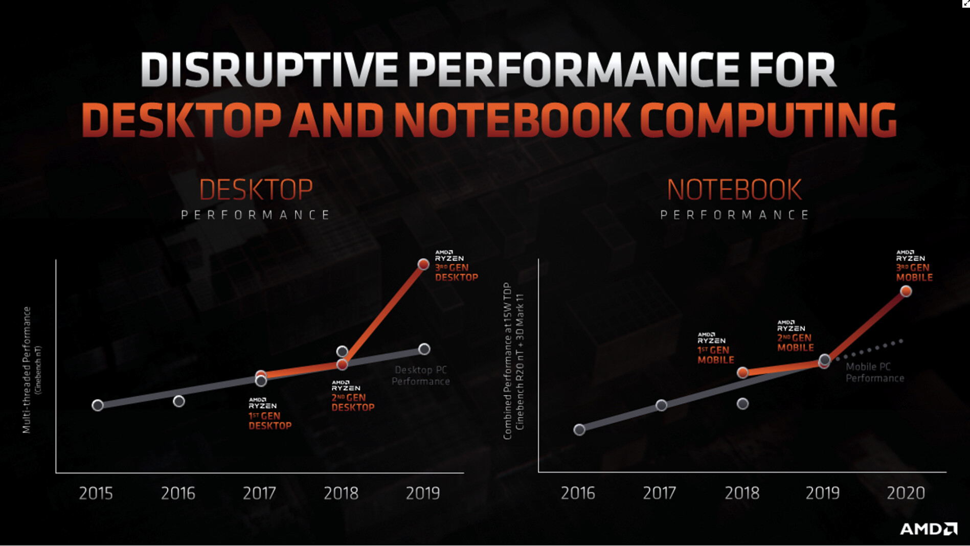
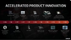 21:10 UTC: When AMD entered the market with Ryzen, suddenly performance went up significantly for both segments. Intel's dominance has been holding back progress.
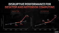
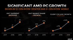
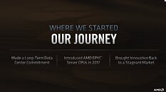
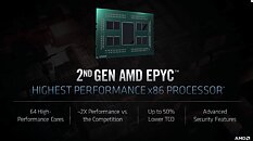
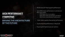
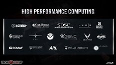
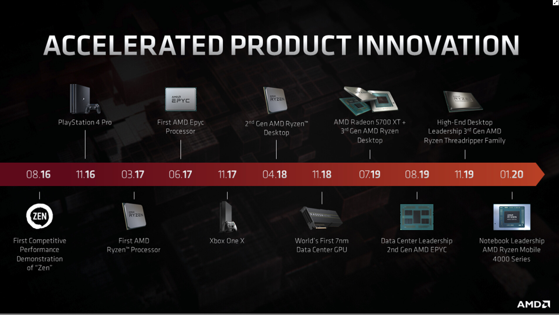
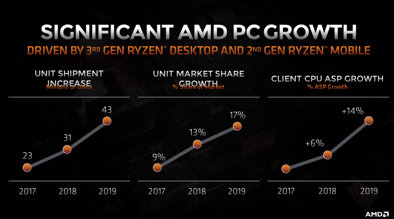
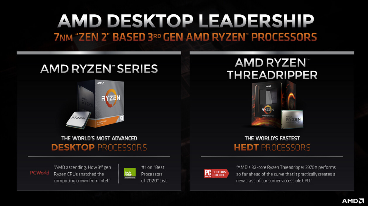
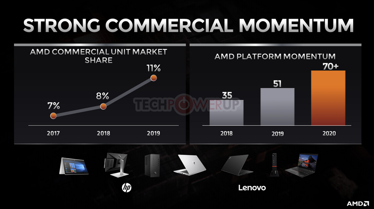
 21:11 UTC: AMD highlights how 2019 was a key year for the company. 8% of market share growth per quarter. "Very proud of Department of Energy supercomputer deployment wins."
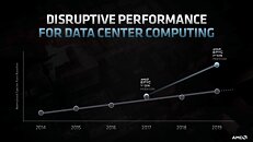
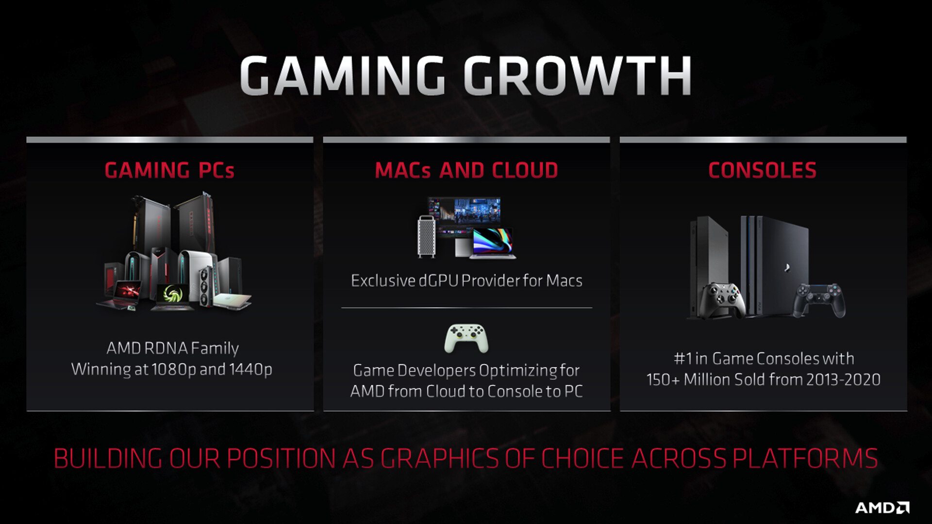
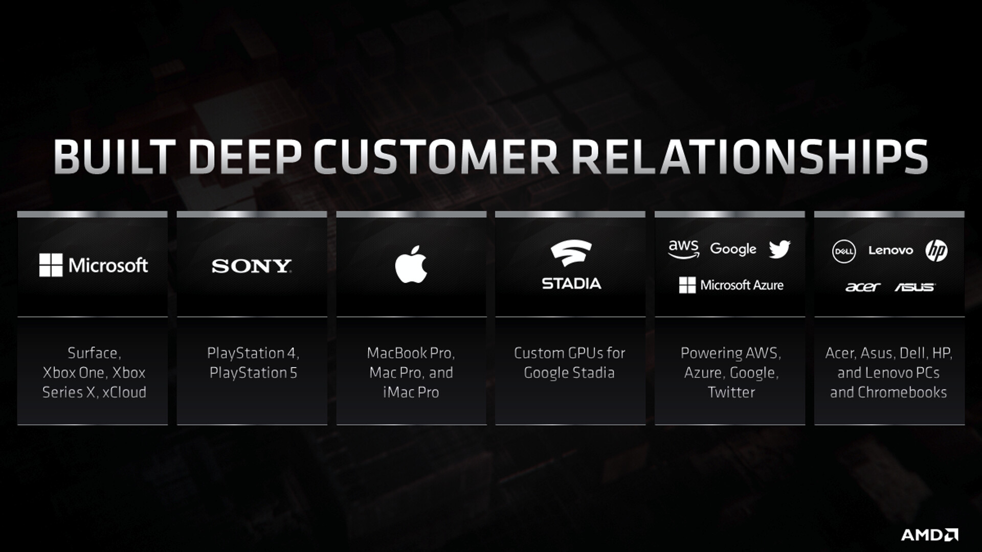
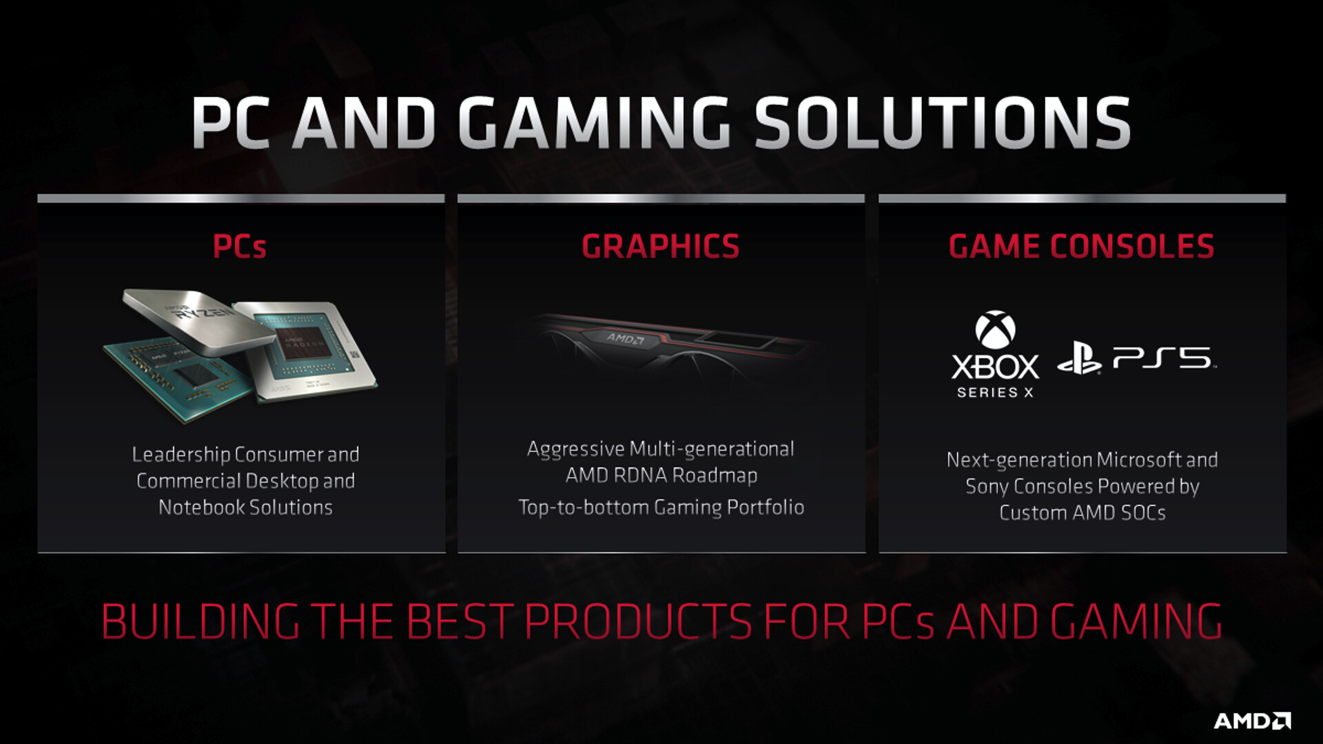
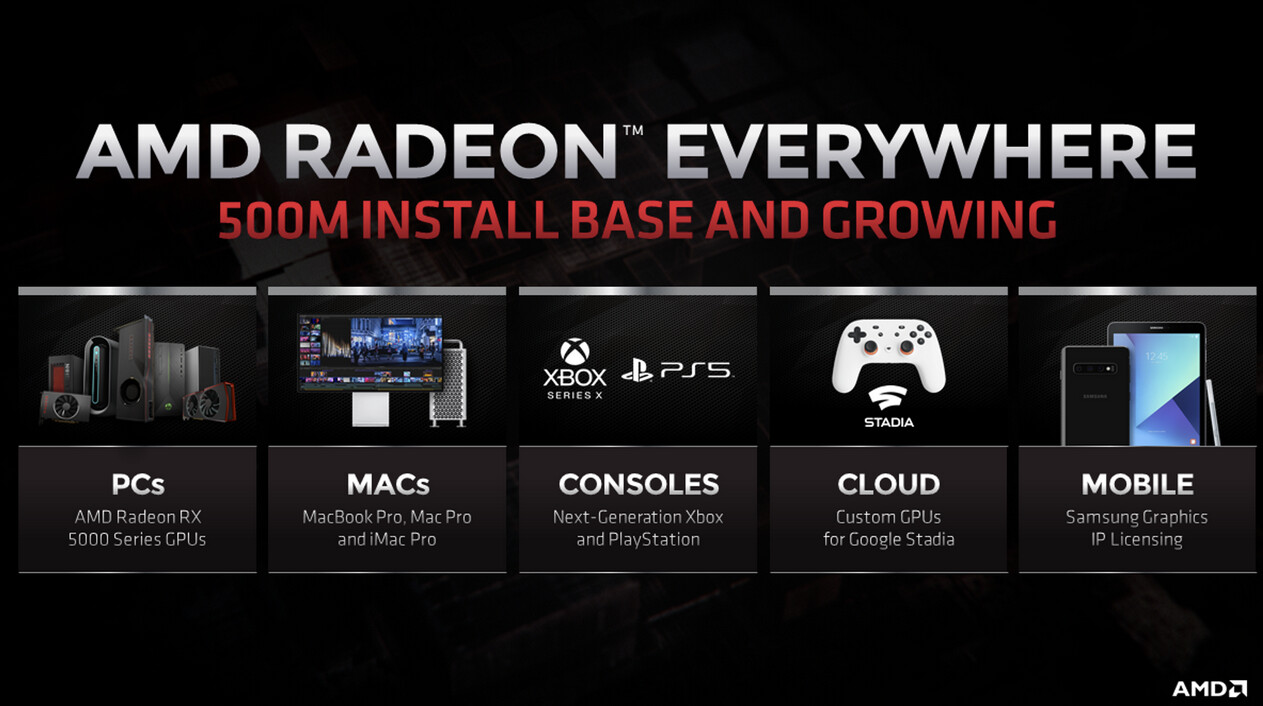
 21:15 UTC: "We're continuing to invest in graphics, winning in 1080p and 1440p". AMD is the exclusive partner for Apple Macs, and lead game consoles.
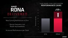
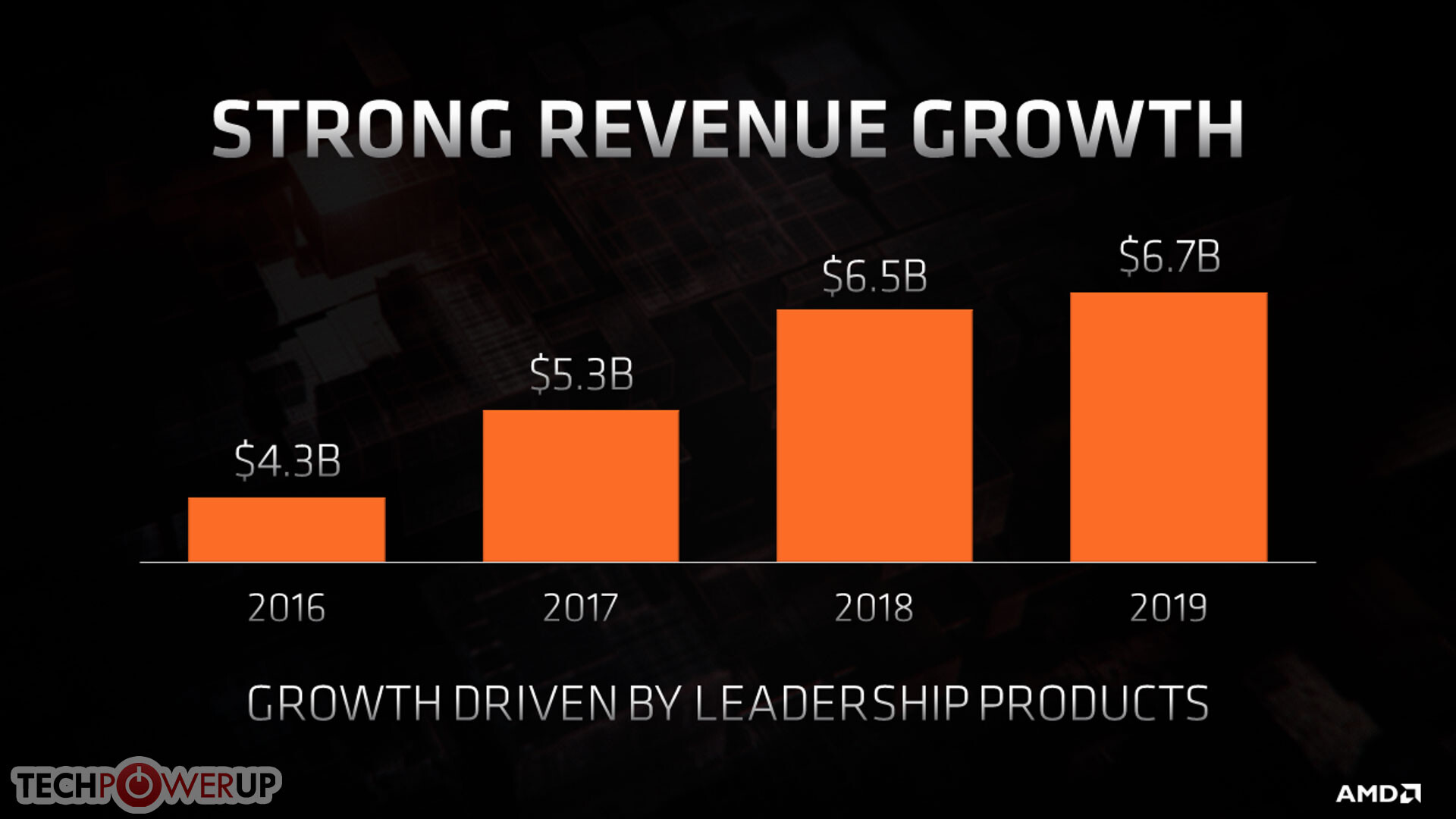
 21:17 UTC: AGR (annual growth rate) detailed. All businesses contributed — roughly 14% year-over-year improvement, every year, since 2015.
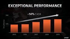
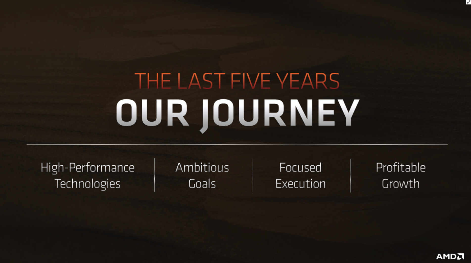
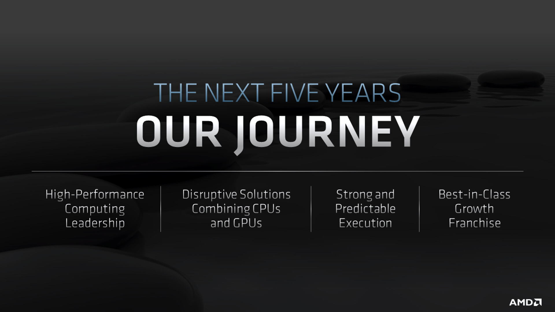
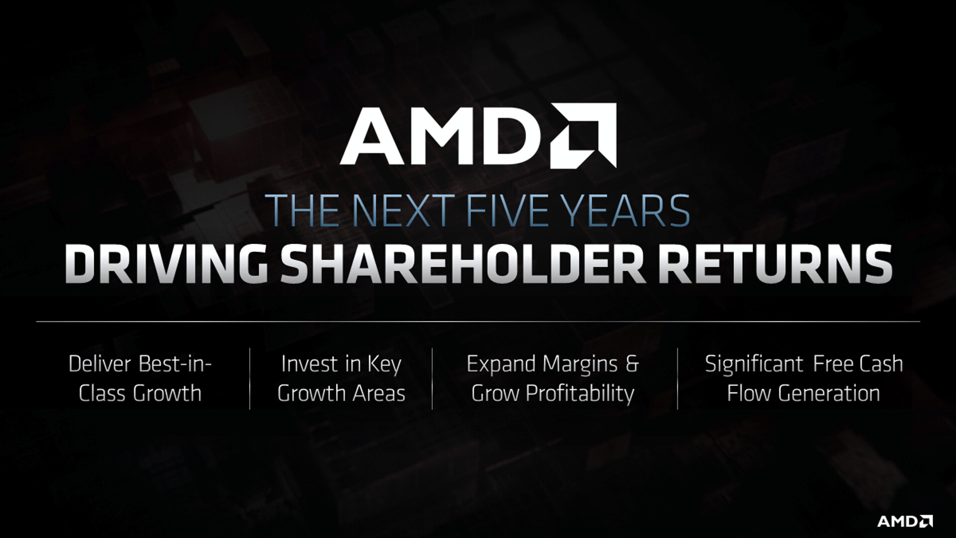
 21:19 UTC: AMD is very optimistic about the next five years, as they focus on expansion in they key market areas.
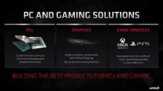
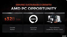
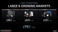
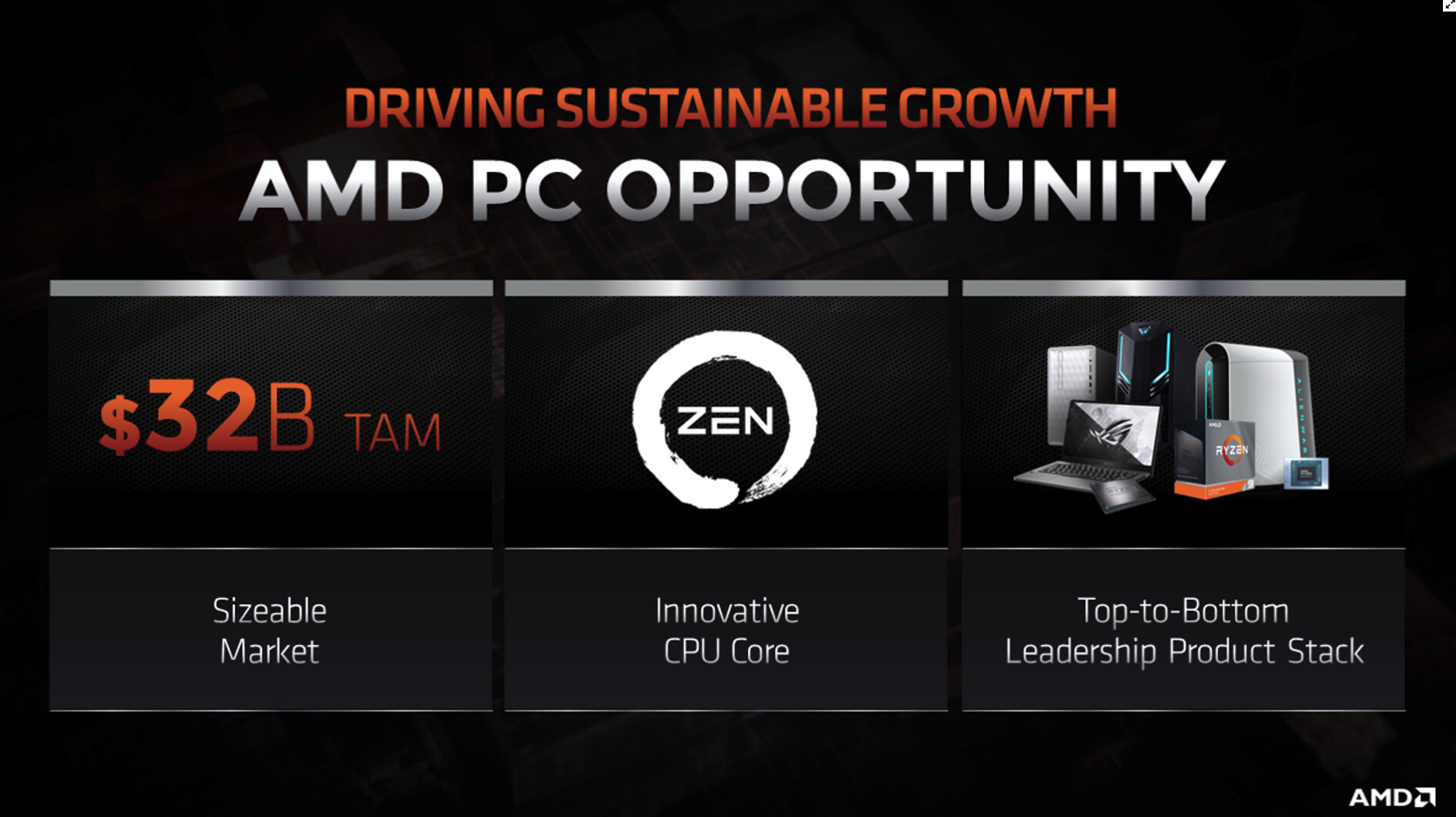
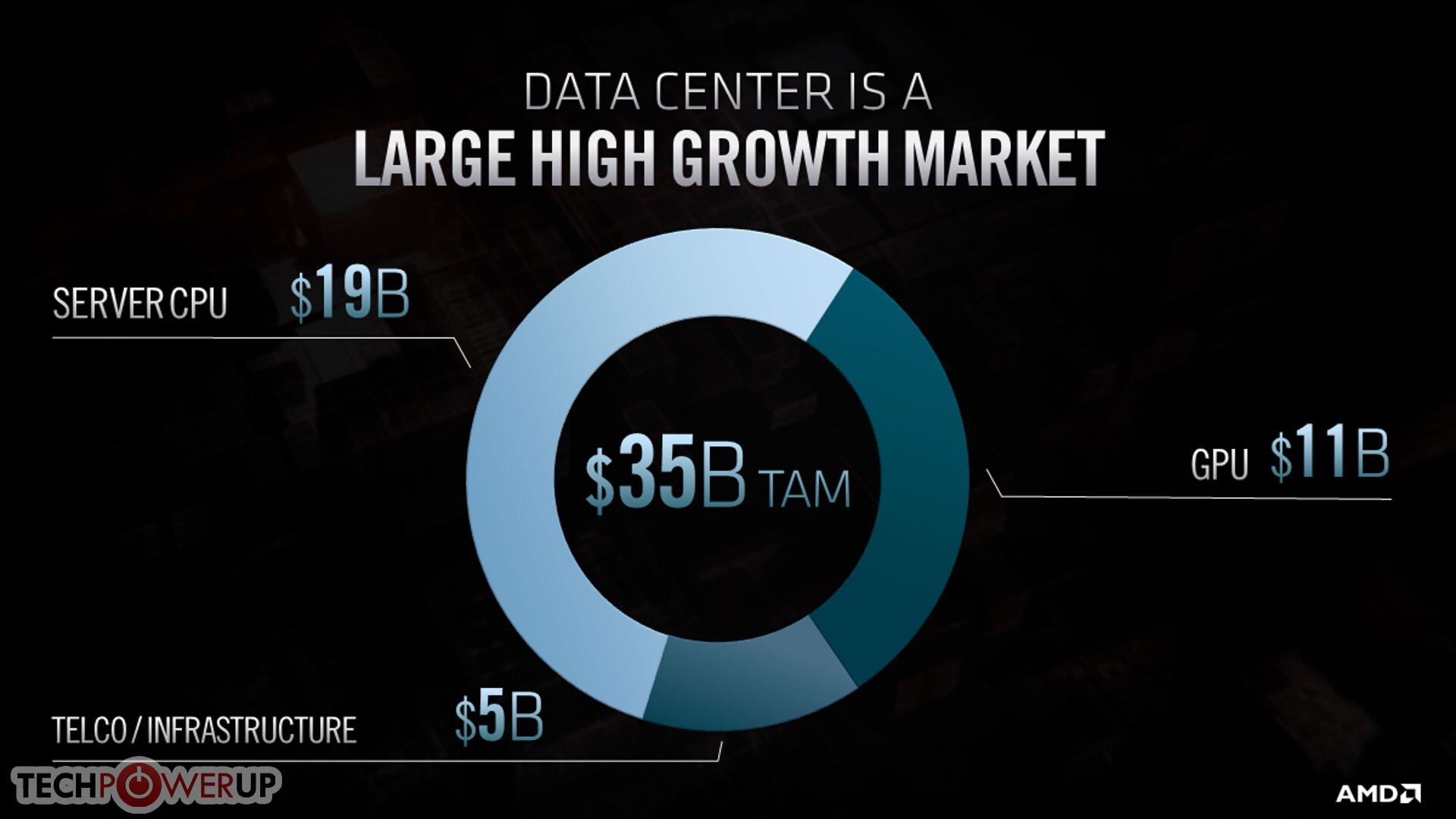
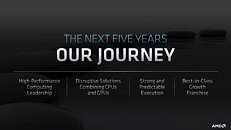 21:21 UTC: AMD recognizes the markets its playing with. Datacenter is worth $35 billion each year, and is mostly untapped for AMD. The PC market at $32 billion per year isn't growing much anymore, but it's a huge market that's important for AMD. Gaming (consumer graphics and game consoles): "we this as a good market, lots of people are gaming, these are exciting opportunities for us".
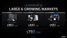 21:22 UTC: Here goes. AMD CEO talks about tech investments on upcoming tech. Zen 3 and RDNA 2 confirmed!
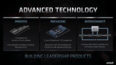
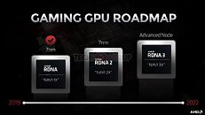
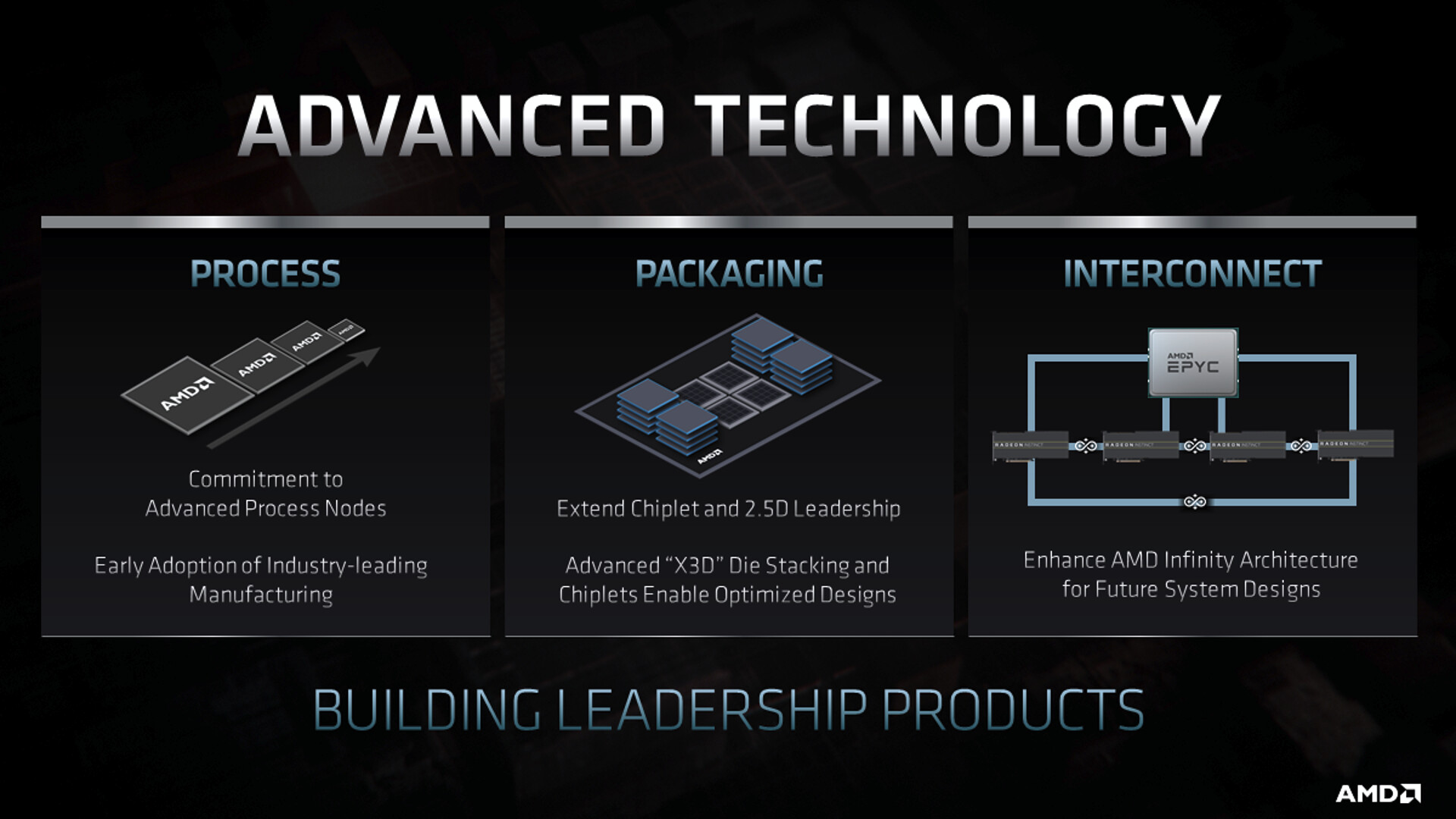
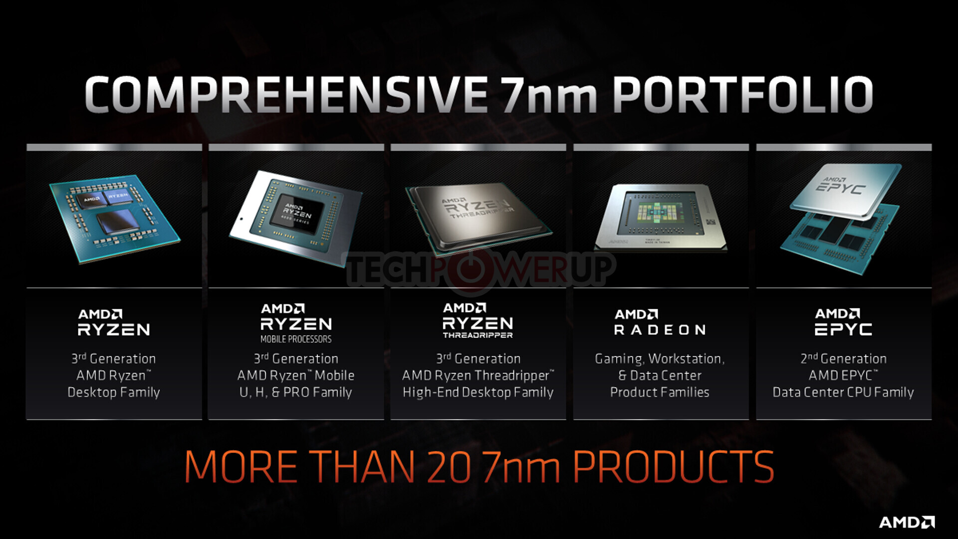
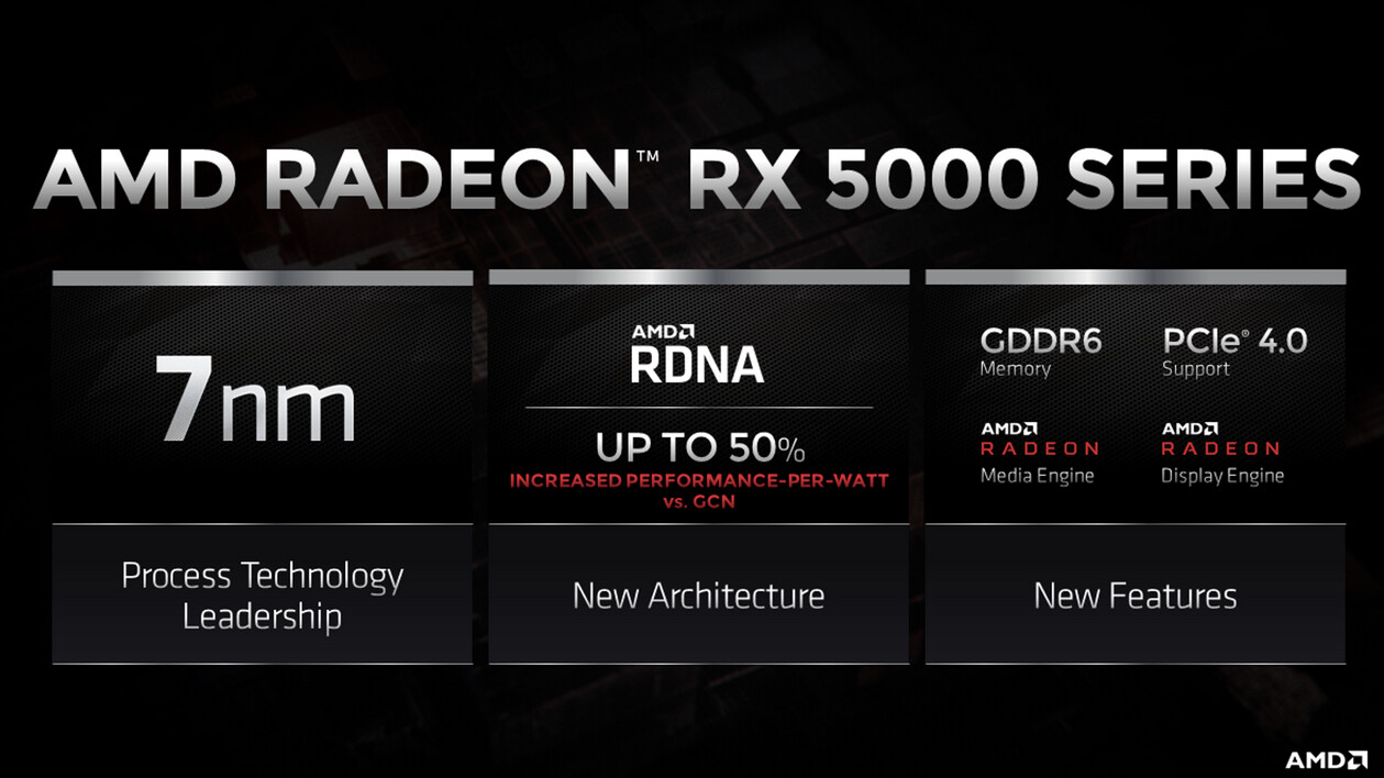
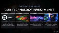 21:23 UTC: AMD talks about Zen 3 on 7 nanometer, and Zen 4 on 5 nm. On the Radeon side, RDNA2 will use 7 nm and RDNA 3 will use an "Advanced Node". Looks like, unlike on the CPU side, they aren't fully decided yet on the fabrication process for RDNA 3. AMD is putting heavy investment in process and packaging, AMD is betting on X3D die-stacking being the next big thing.
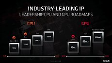
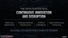
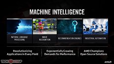
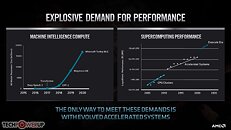
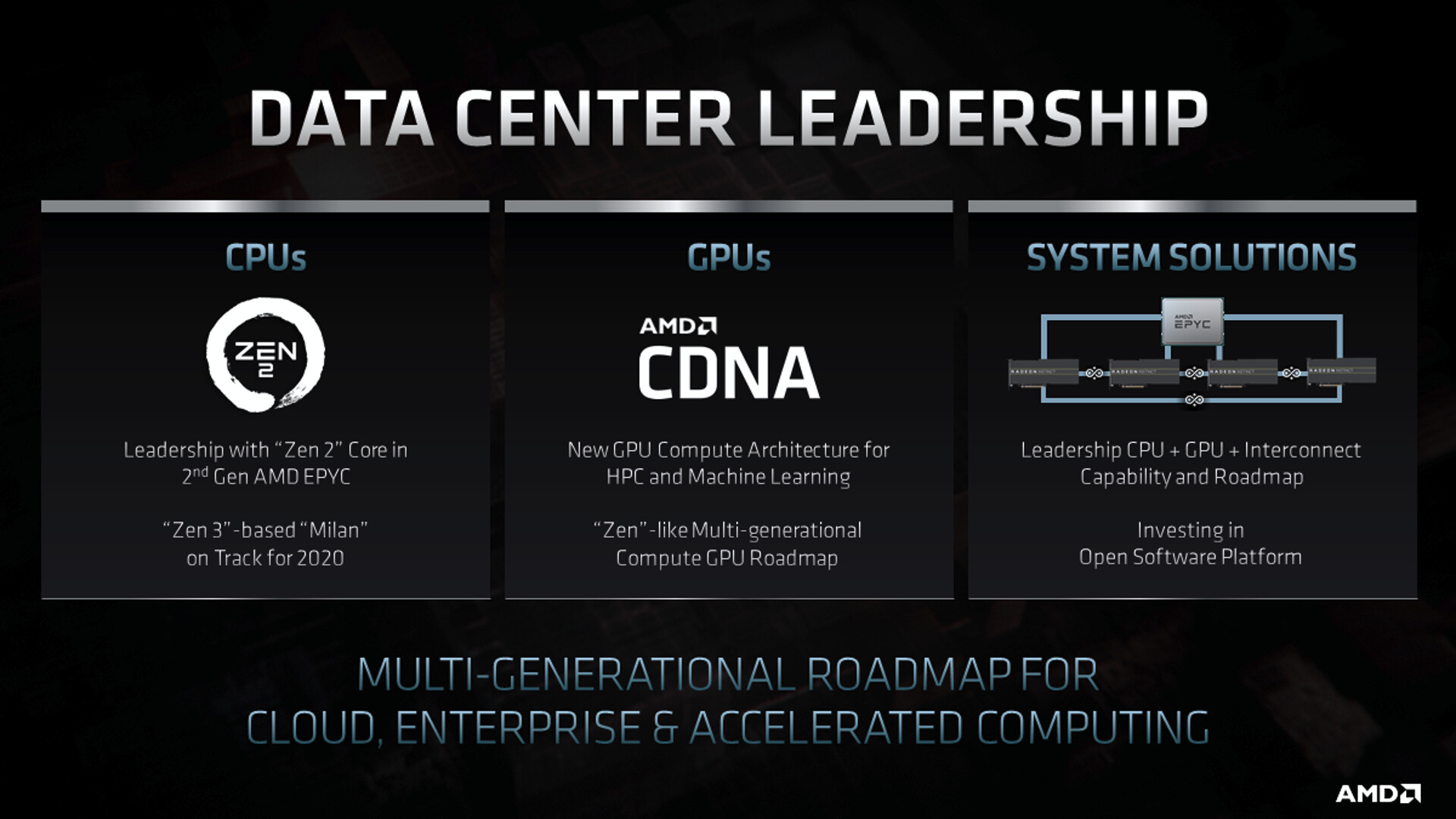
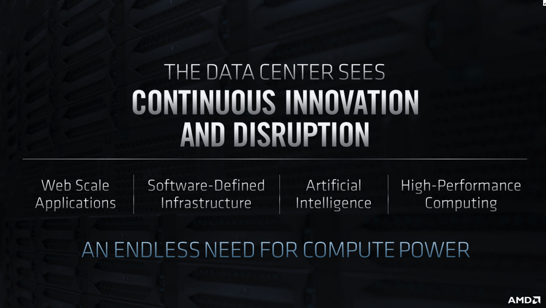
 21:25 UTC: There is an insatiable demand for compute in the data-center market. Computation model sizes are growing tremendously.
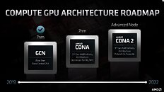
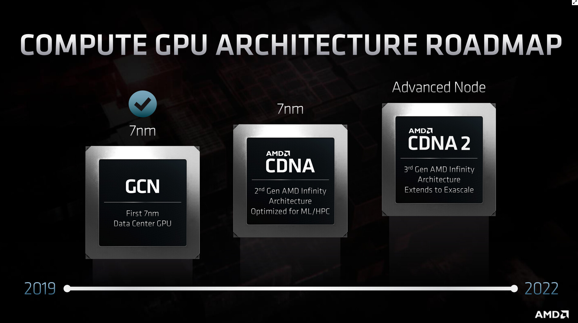
 21:26 UTC: For the datacenter AMD is preparing a new architecture called "CDNA", for GPU-based compute accelerators. GPUs without raster hardware is happening.
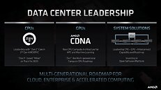 21:28 UTC: AMD is adding value to the PC market. Note the image in the middle, under "graphics". Is this the new AMD VGA reference design? Looks like the company is finally moving away from blower coolers!
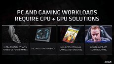
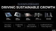
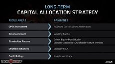
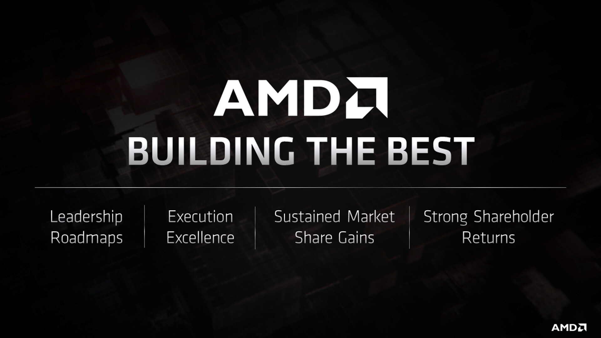
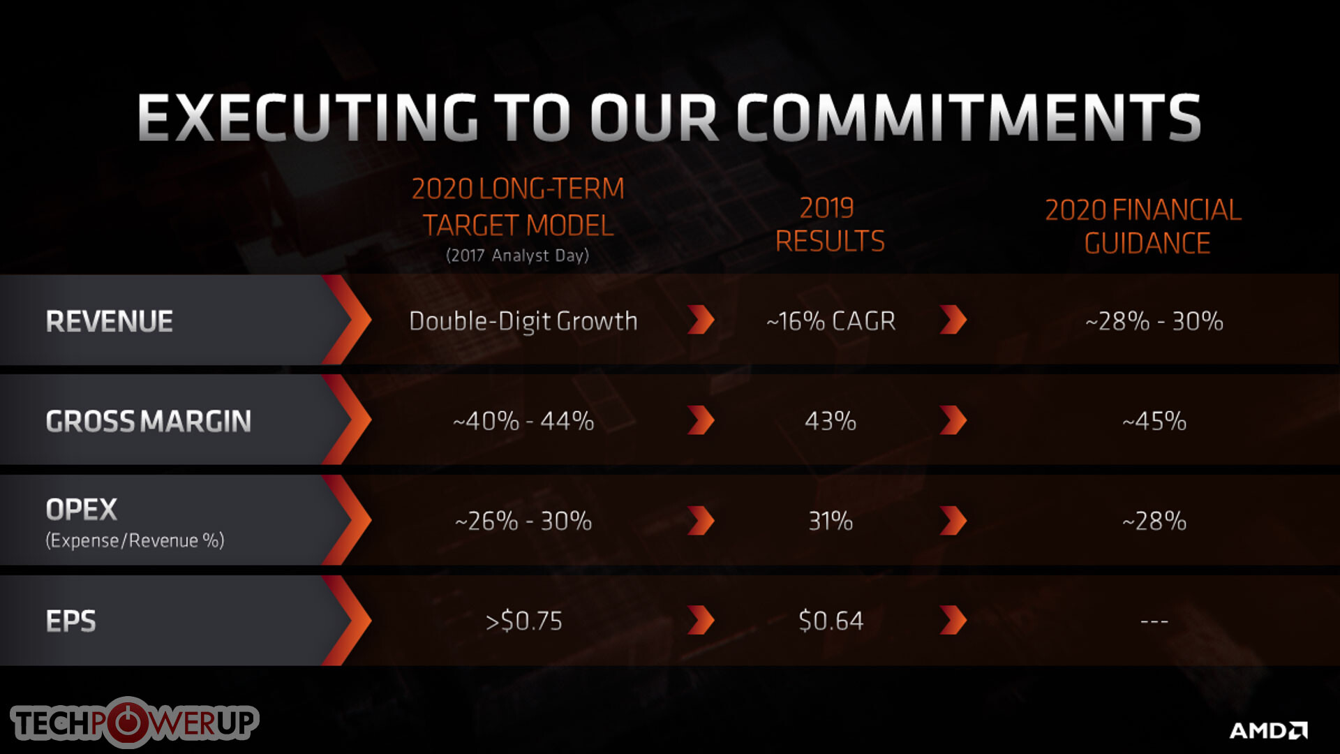
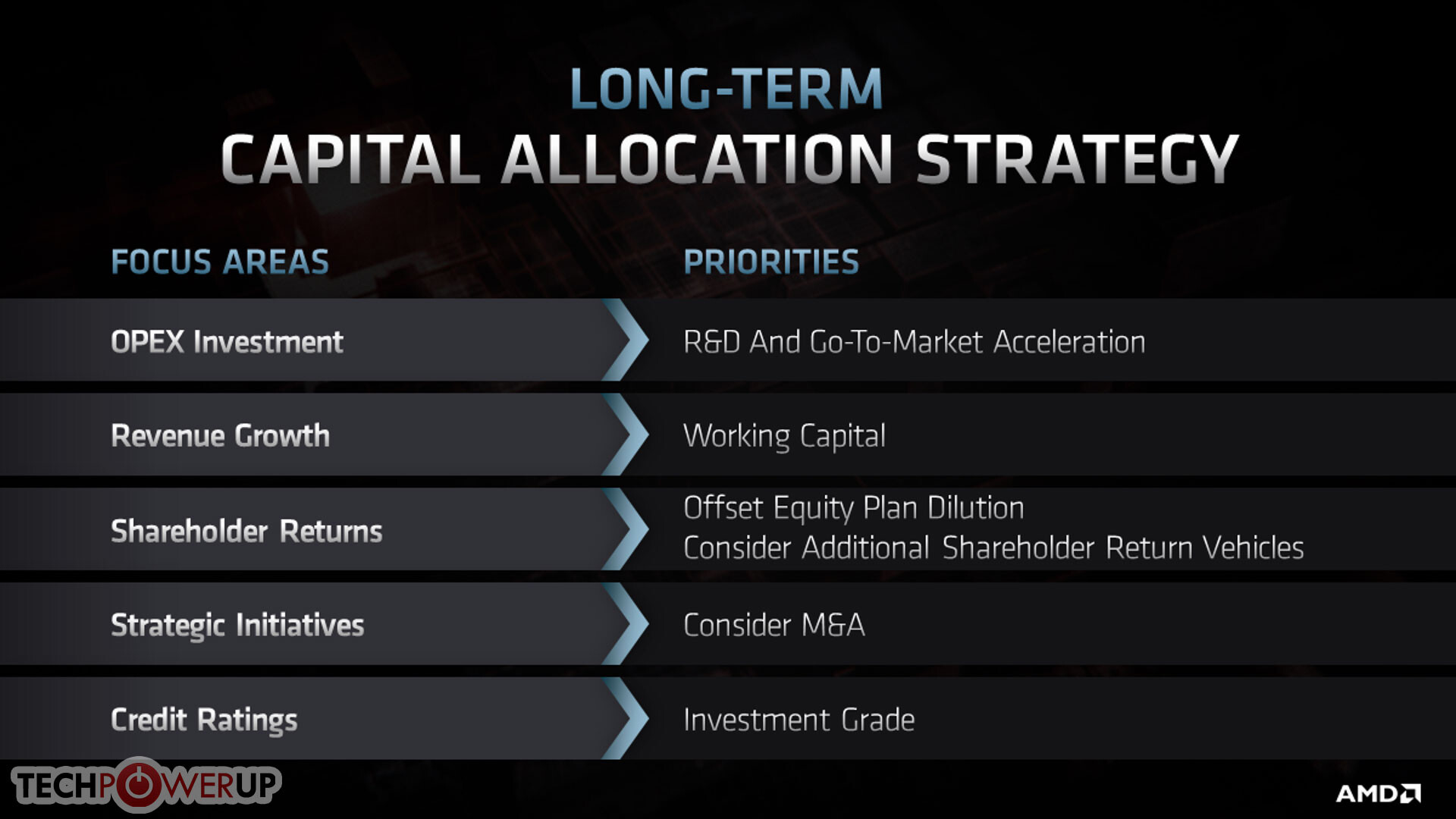
21:30 UTC: AMD has a strategy in place to drive shareholder returns over the next 5 years.
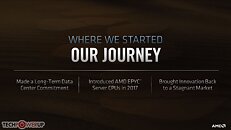
21:32 UTC: What was unrealistic/ambitious in 2017 is realistic now.

21:35 UTC: CTO Mark Papermaster takes stage. Talks about reengineering of the engineering approach at AMD.
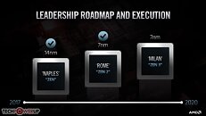
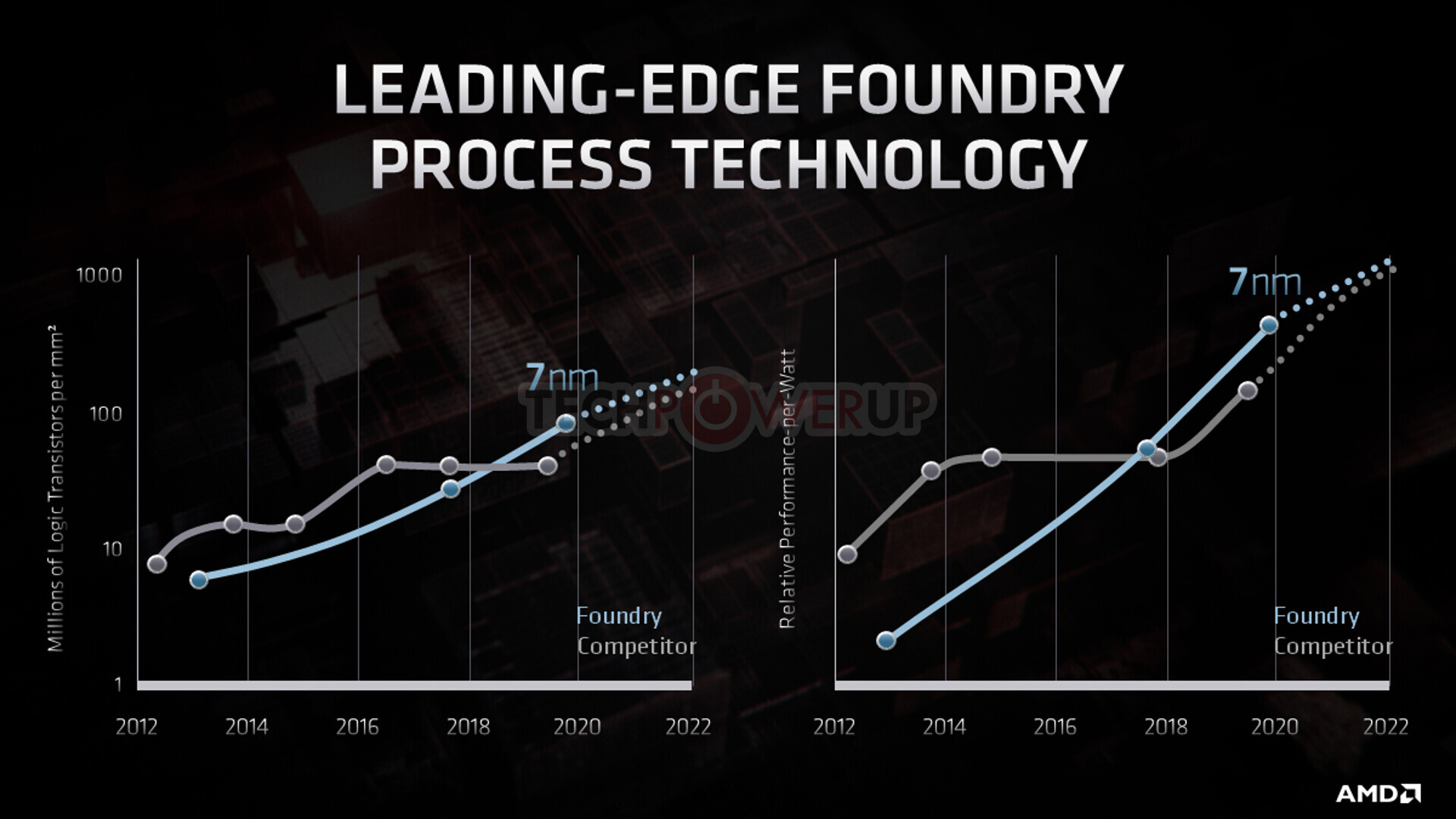
 21:46 UTC: AMD 7 nm execution detailed.
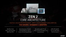
 21:47 UTC: AMD is confident that they process technology will be able to compete with Intel's upcoming 7 nanometer tech.
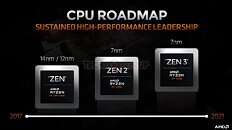
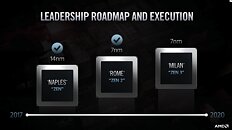
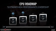
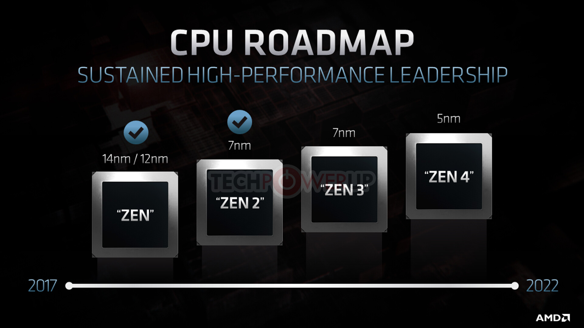
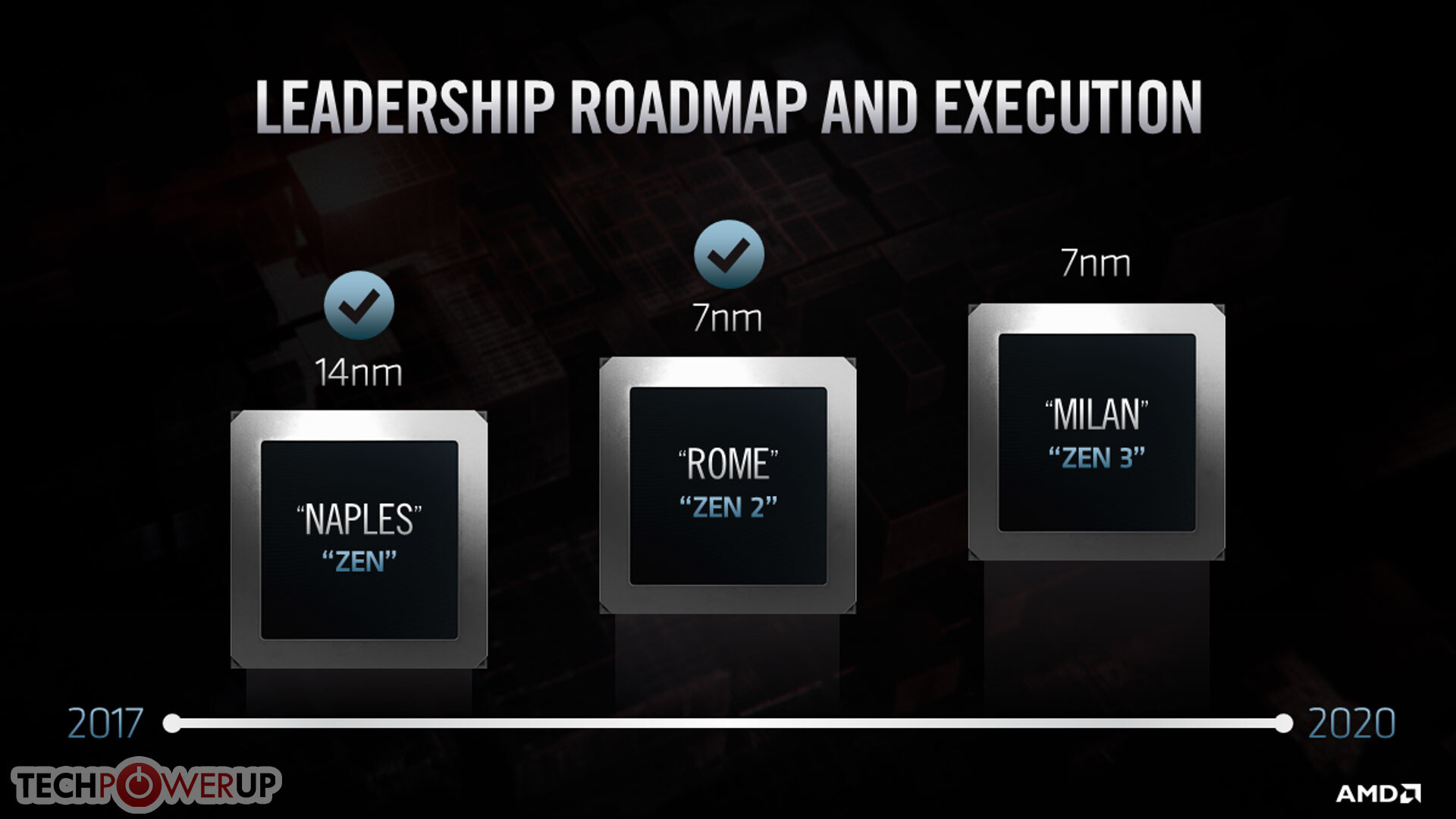
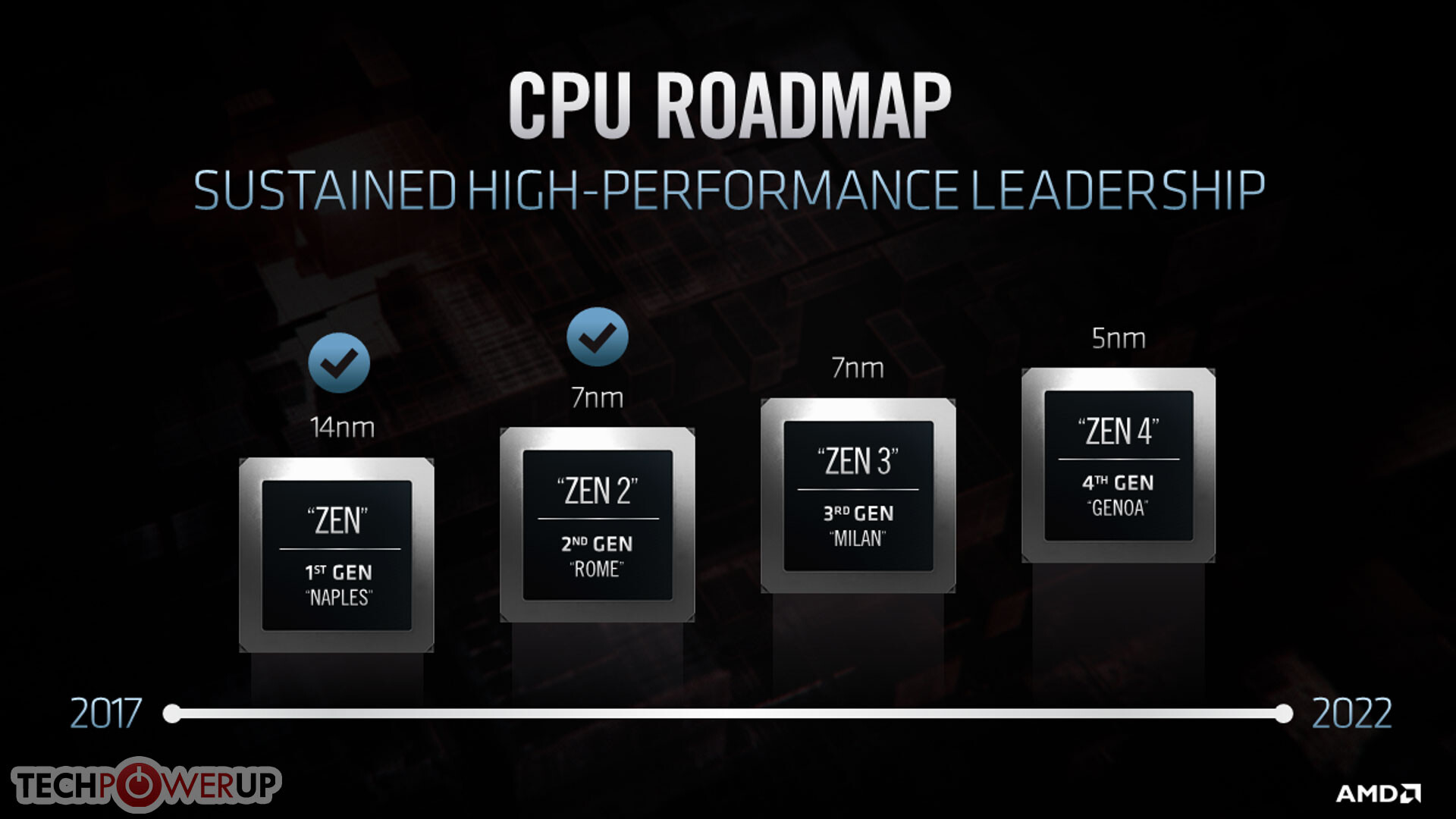
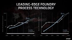 21:48 UTC: The AMD CPU roadmap is detailed for the years leading up to 2022. Here we see Zen 3 on 7 nanometer, and Zen 4 on 5 nanometer, both at TSMC. AMD is aware that their competition isn't resting, so they're investing a lot into future technologies.
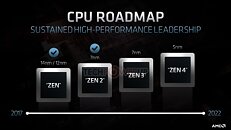
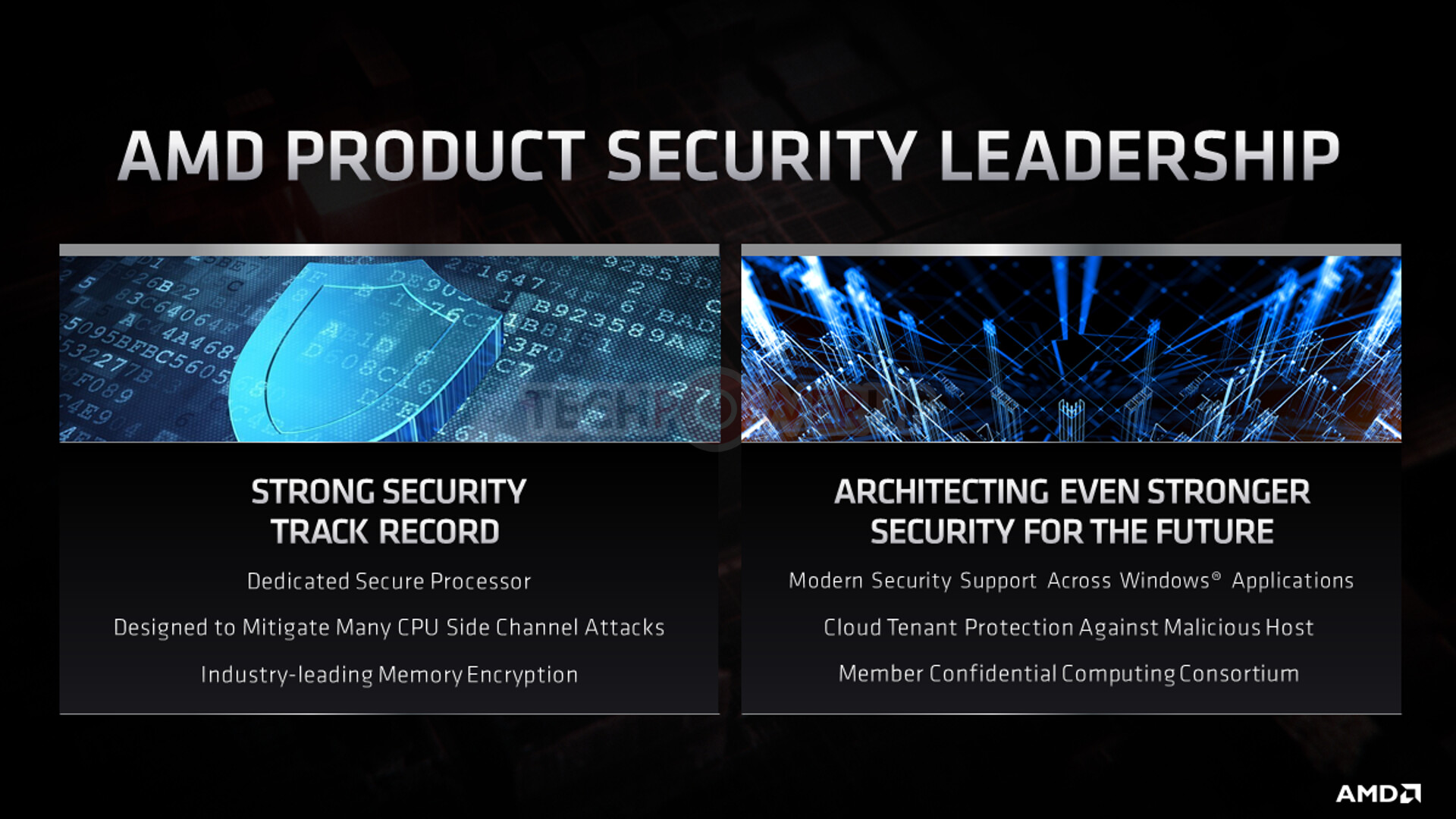
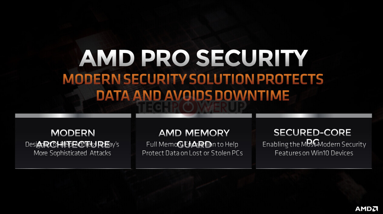
 21:49 UTC: Papermaster takes a moment to talk about superior CPU security. AMD microarchitectures largely immune to side-channel attacks. AMD implements memory encryption.
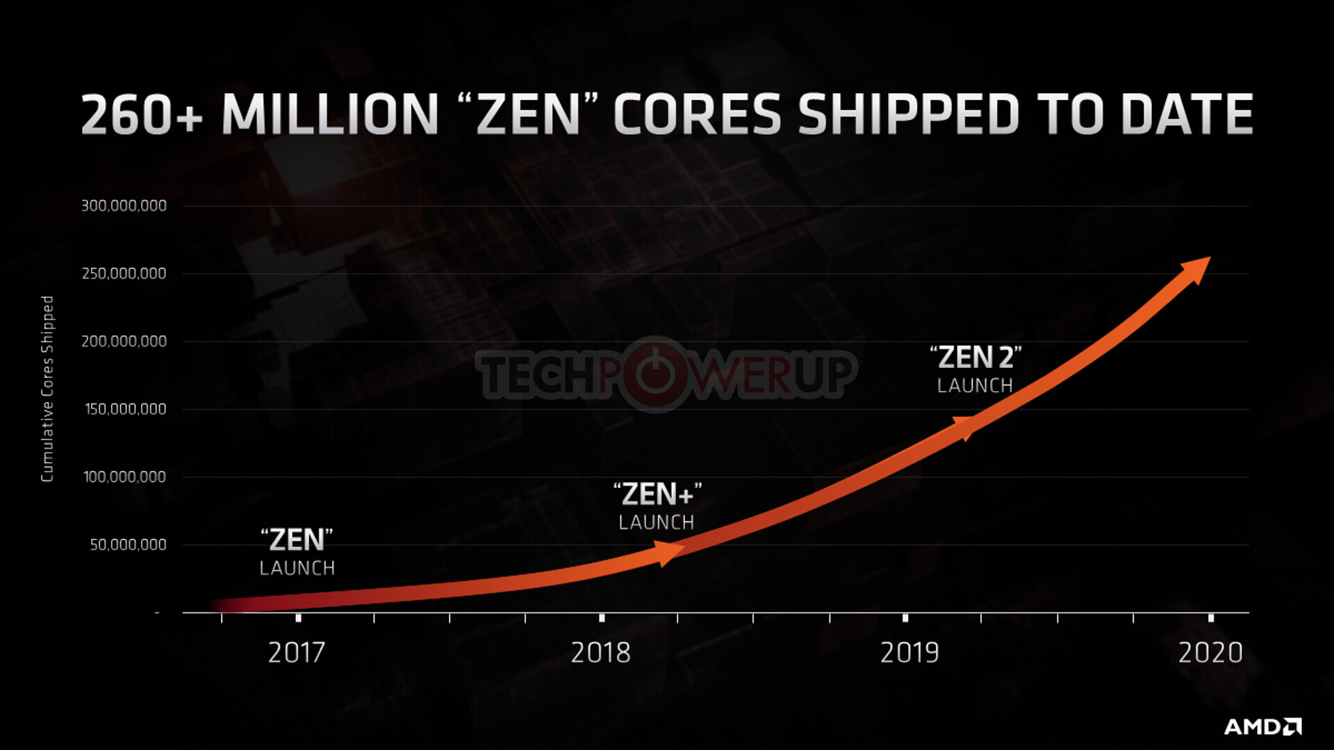
 21:50 UTC: AMD has shipped 260 million+ Zen cores shipped to date!
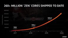
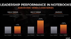
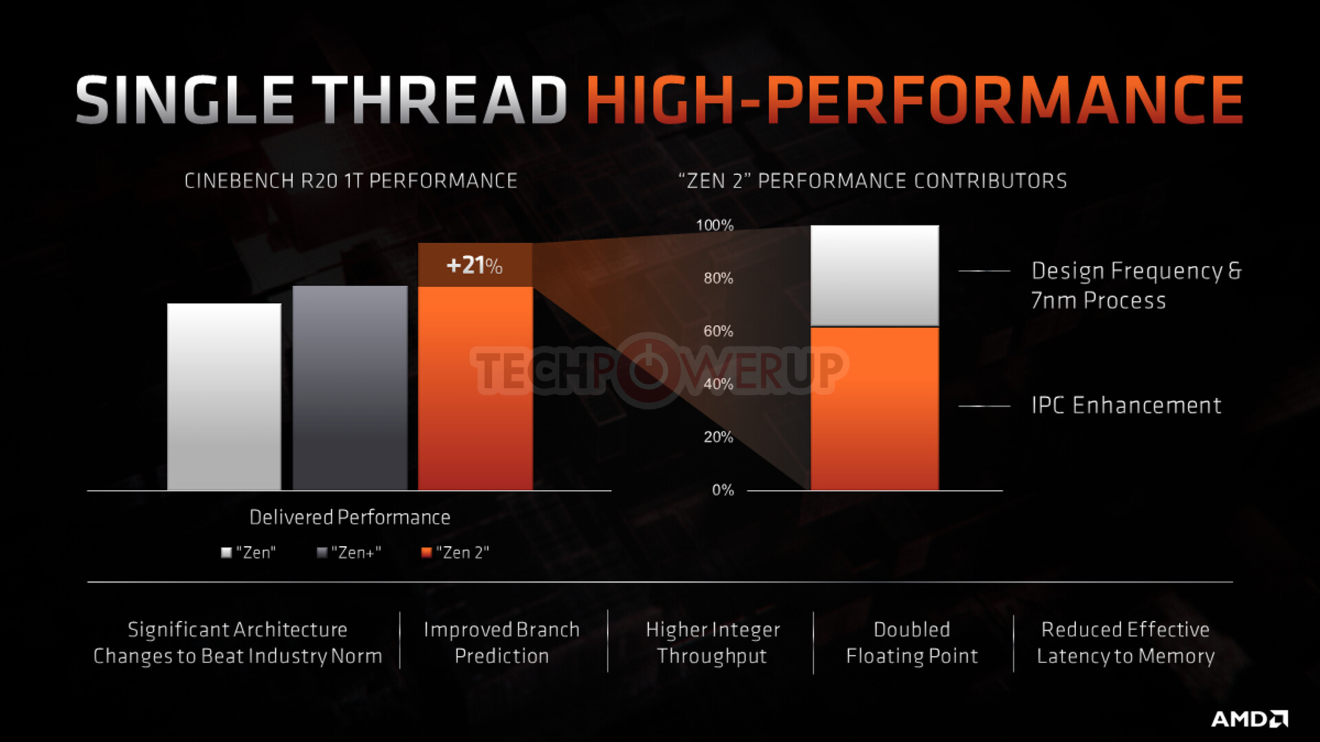
21:51 UTC: AMD is committed to improving IPC of its processors. They're reporting on their single-threaded performance gains, and how they were achieved.
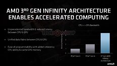
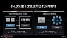
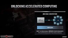
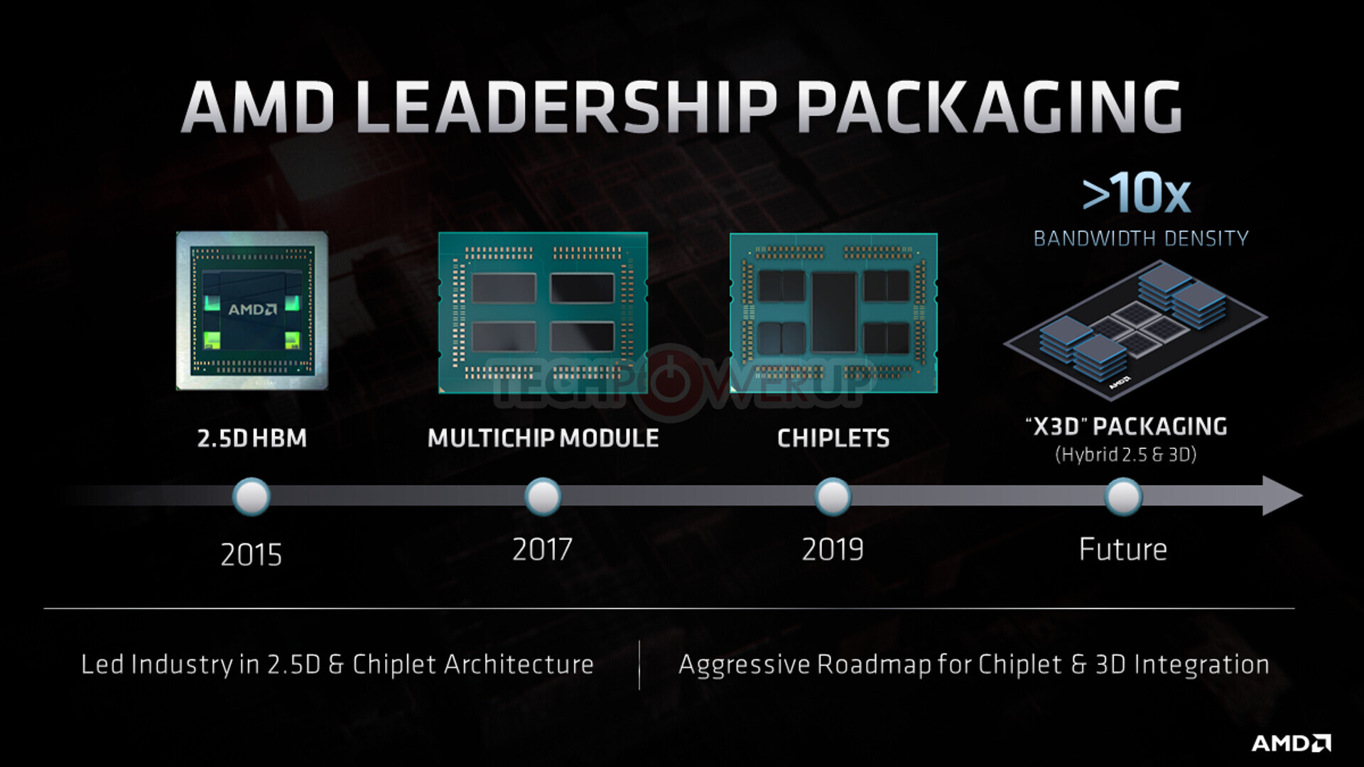
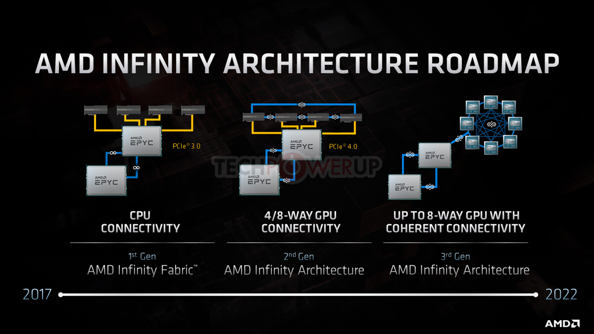
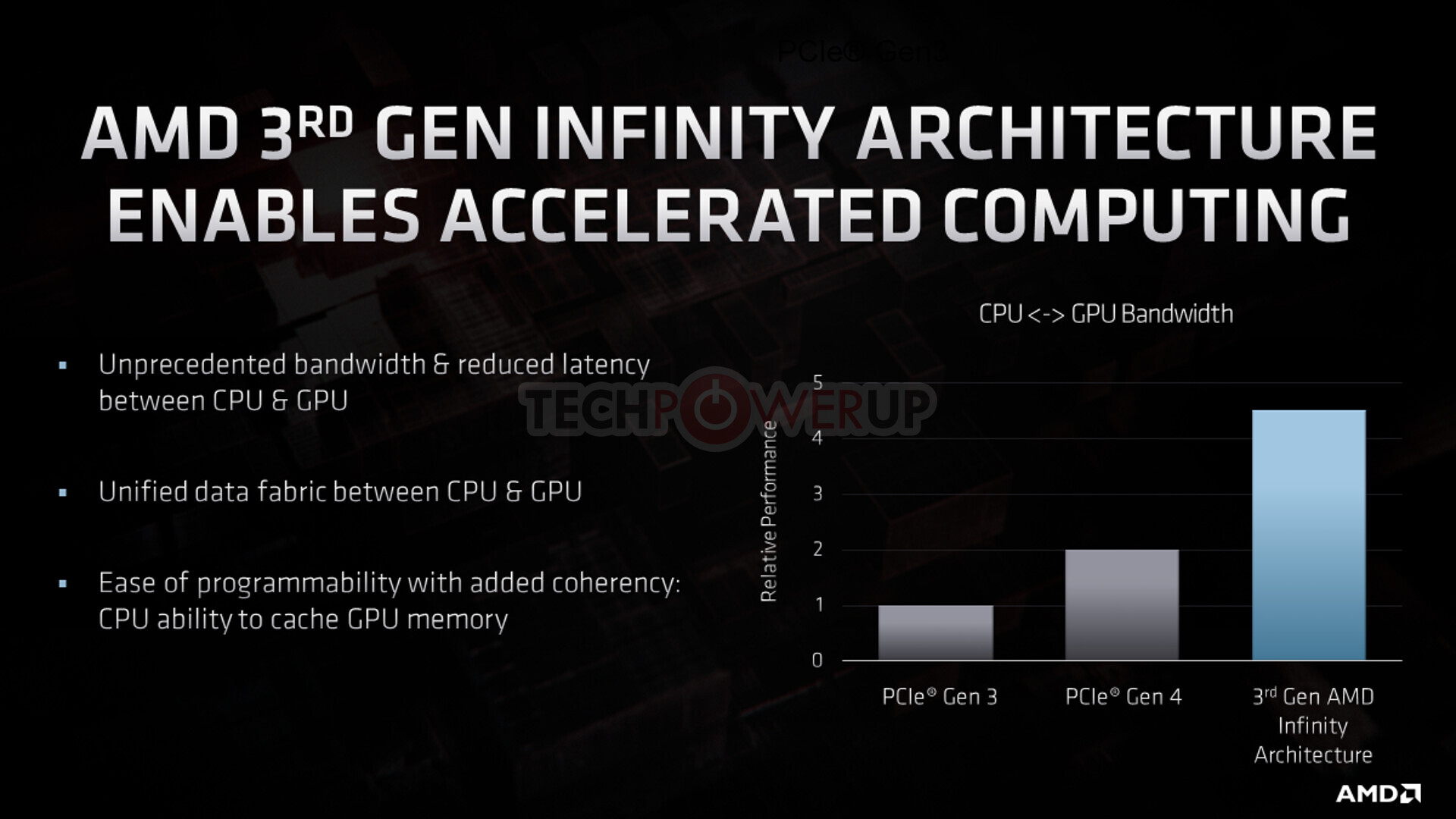
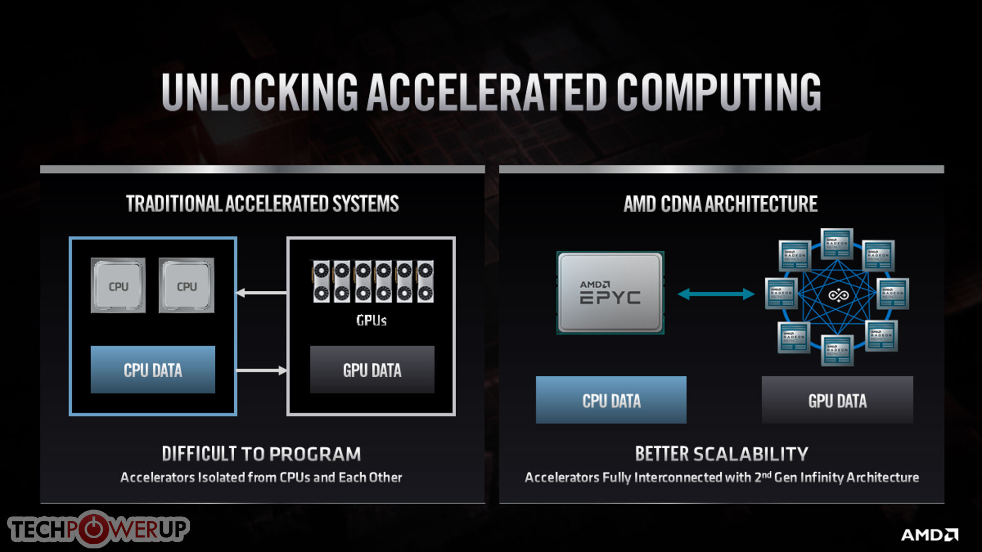
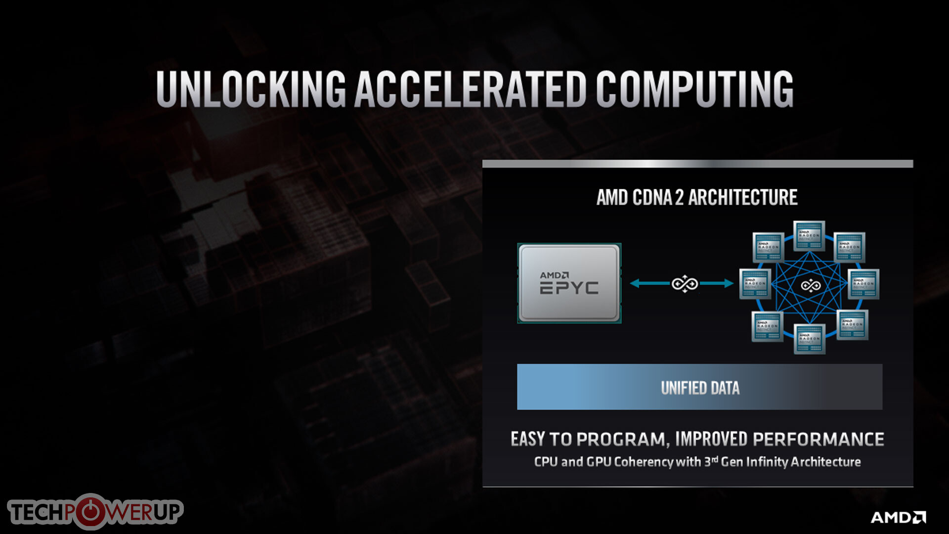
21:54 UTC: Papermaster now goes into more detail regarding future technologies. AMD's packaging innovations are a response to Moore's Law "slowing down". X3D packaging could be AMD's response to Intel Foveros. A step up from 3D packaging.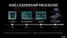 21:55 UTC: Bringing it all together is 3rd gen Infinity Fabric with more scalability and coherency. Also it has unified memory pools, starting with 3rd gen Infinity Fabric. What's interesting here is that AMD is no longer talking about "Infinity Fabric", but is now using the term "Infinity Architecture", to describe all silicon products that use IF technology in one way or another.
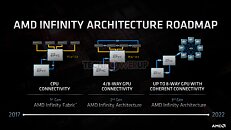
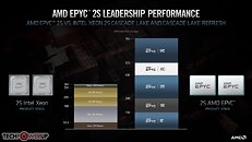
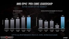
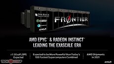
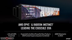
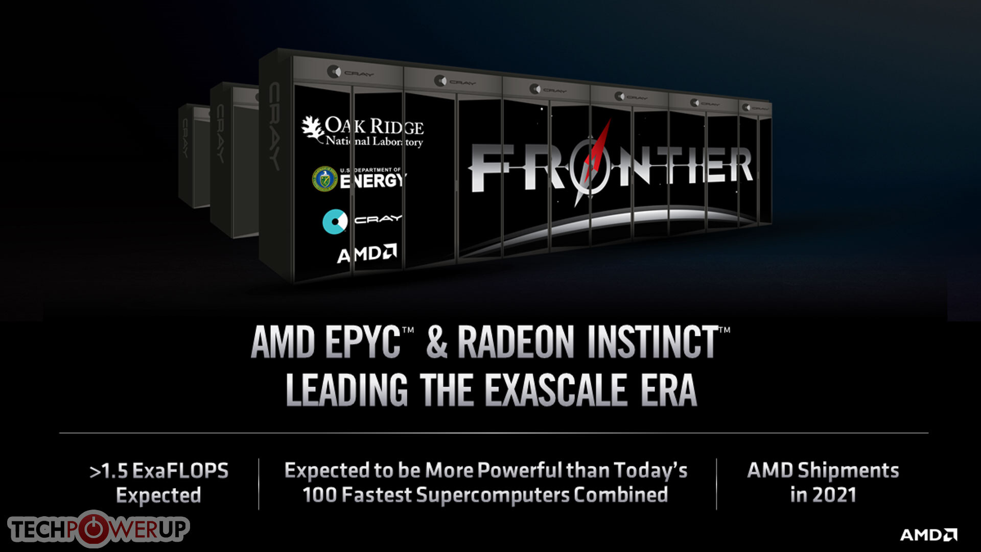
 22:02 UTC: Culmination of all of AMD's scalability tech puts it ahead in the HPC competition.
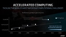
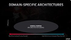
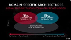
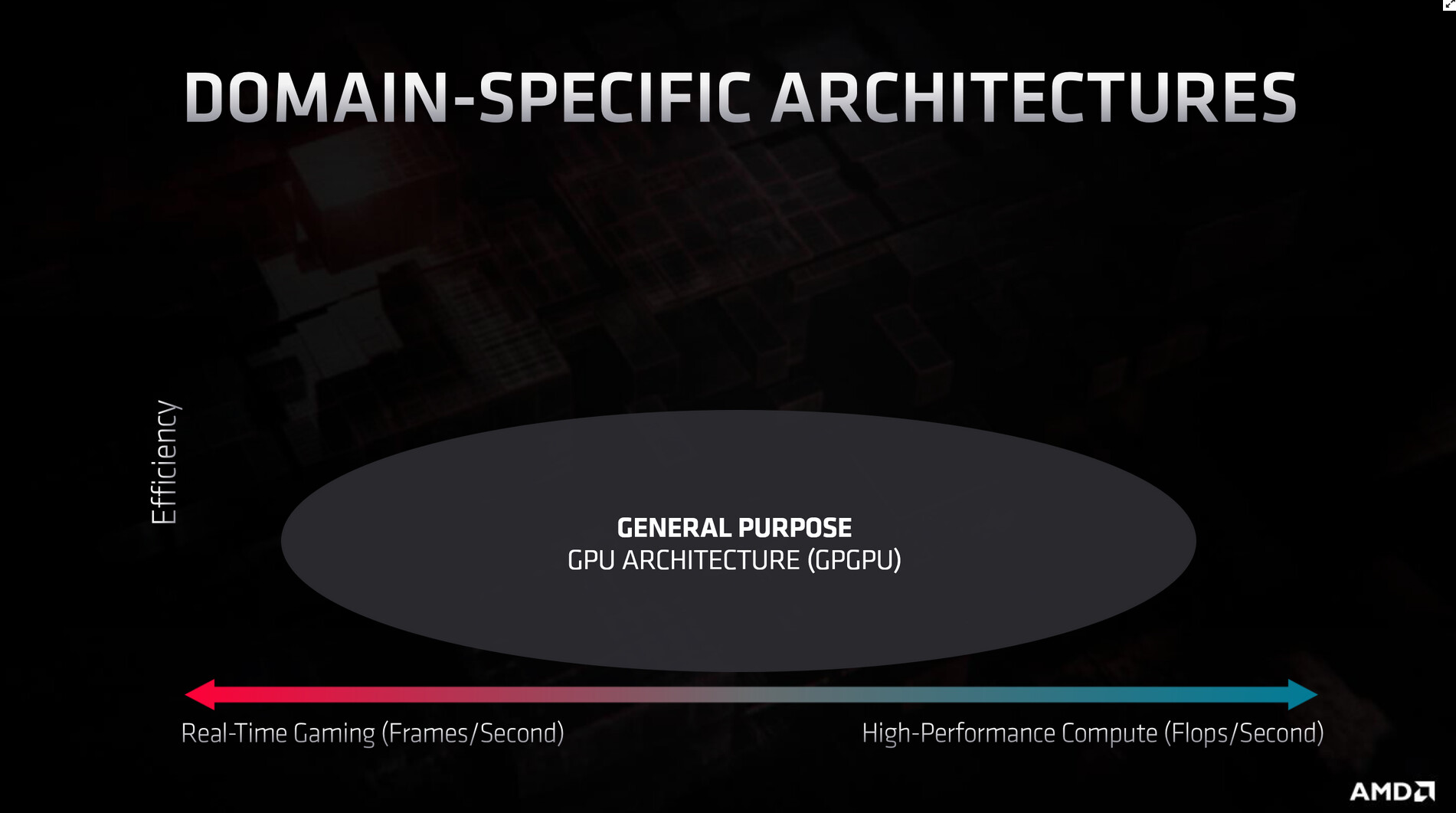
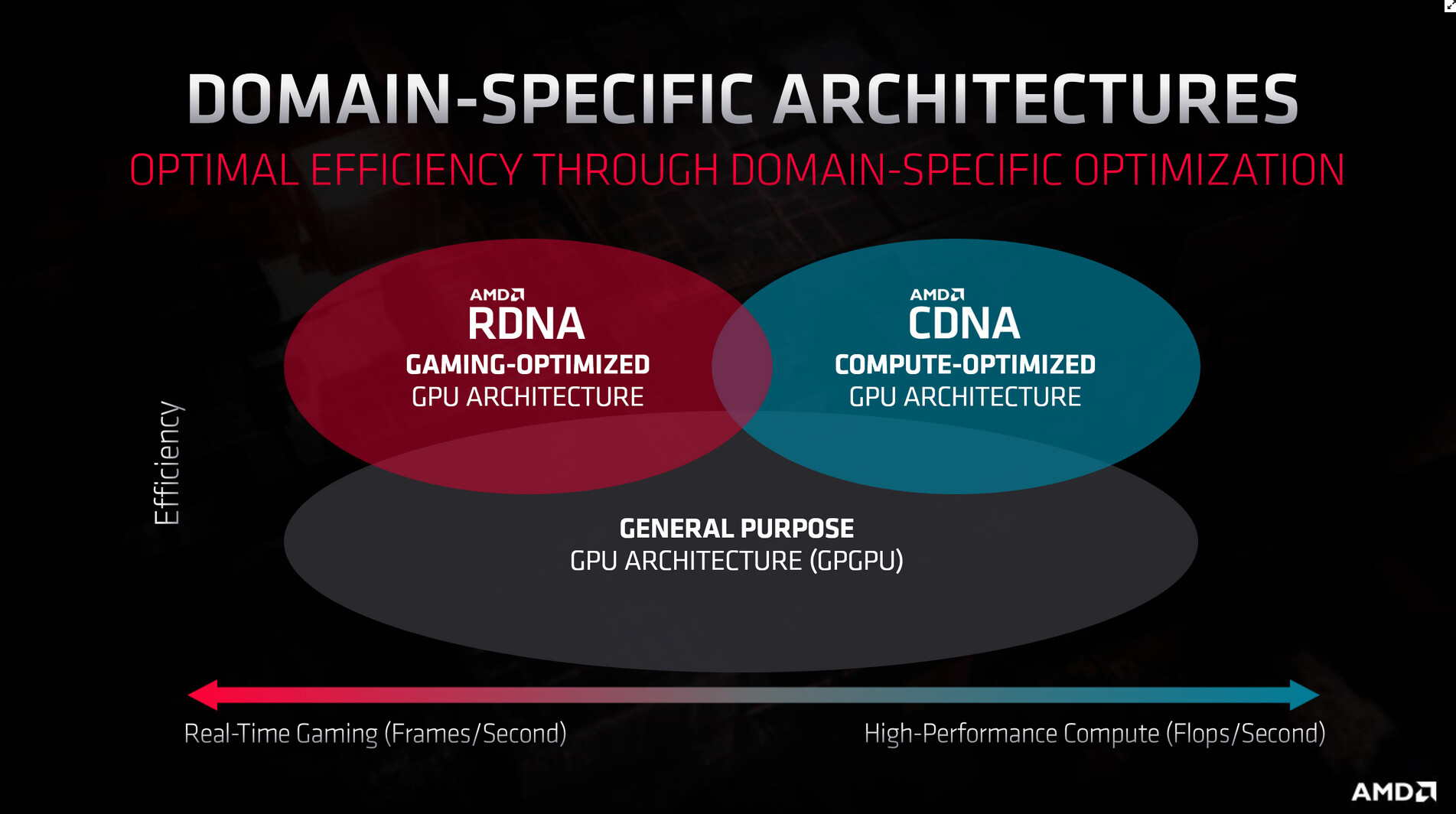
22:05 UTC: Next up: Graphics. David Wang of Radeon Technology Group takes center stage and introduces their strategy looking forward. AMD is the first company to introduce domain-specific architectures: RDNA is for gaming, CDNA is for compute.
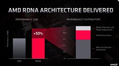
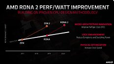
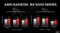
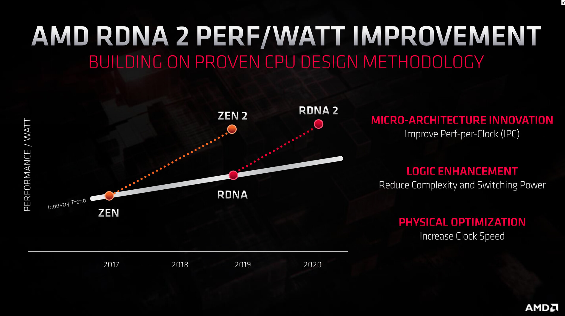
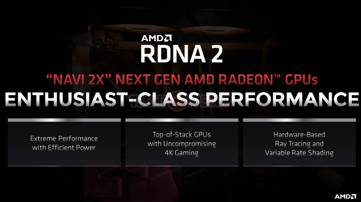
22:13 UTC: 50% performance improvement over RDNA with RDNA2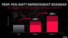
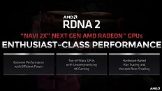
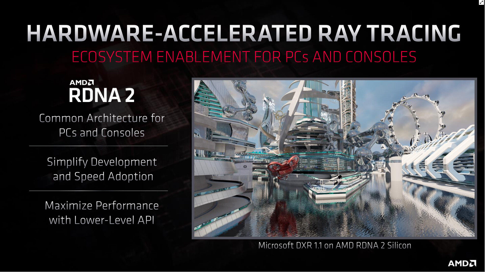
22:10 UTC: Details on RDNA now and tomorrow. RDNA2 has Variable Rate Shading and native support for hardware-accelerated ray-tracing.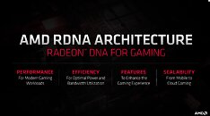
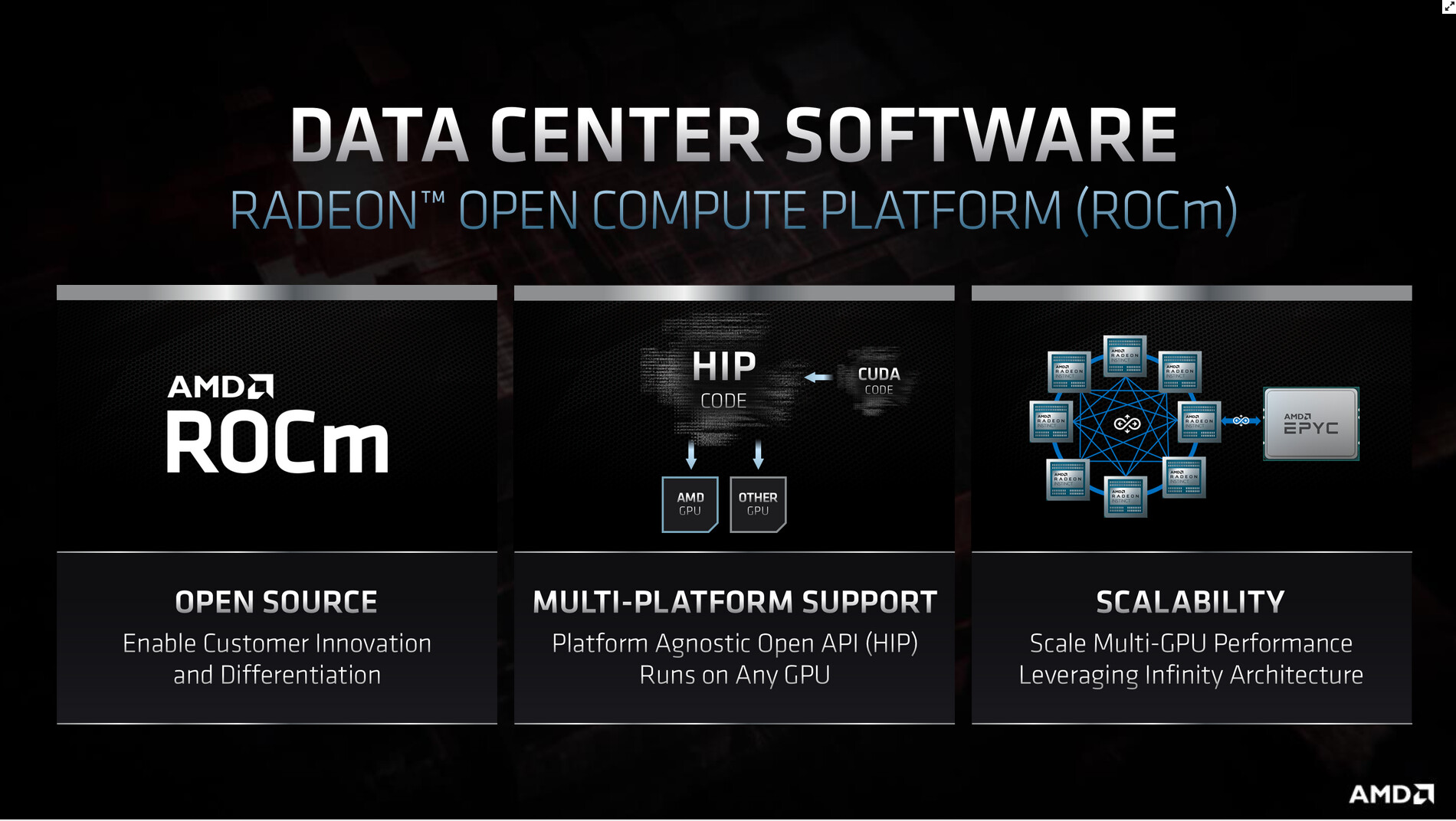
22:14 UTC: All new RDNA2 based hardware-accelerated ray-tracing architecture, leverages DXR 1.1, which is a new revision of Microsoft's DirectX Raytracing API. The slide also shows a screenshot of raytracing running on AMD's RDNA2 silicon.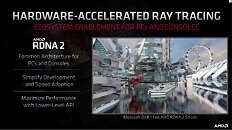 22:15 UTC: AMD's CDNA architecture is compute-optimized, removes all raster hardware. Adds tensor hardware to help AI. Highly scalable. Backed by open-source software, unlike NVIDIA. Existing CUDA code can be converted with HIP code converters.
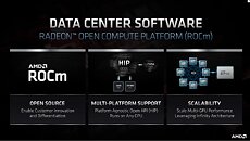
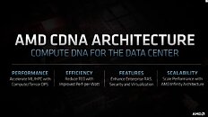

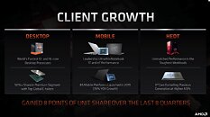
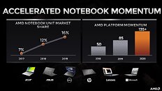
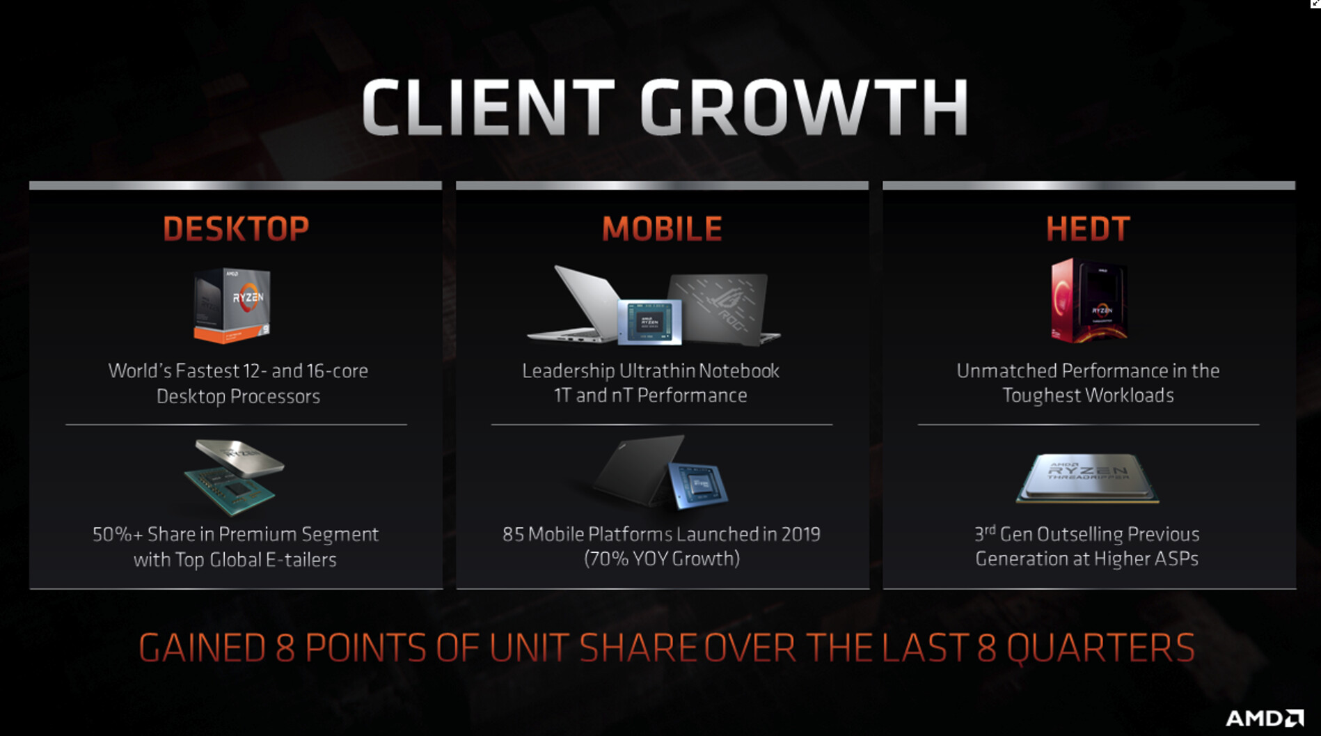
22:24 UTC: AMD PC business overview.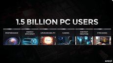

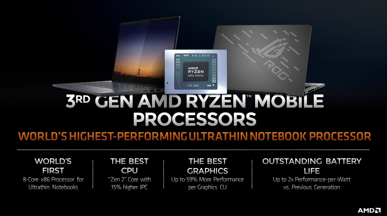
22:30 UTC: AMD has big plans to grow its CPU market share in notebooks, across all form-factors.

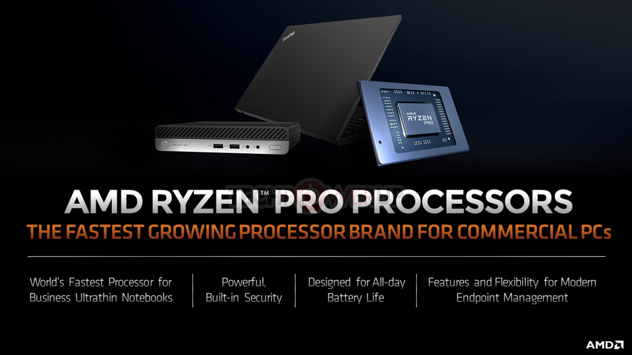
22:33 UTC: AMD talks mobile security, Ryzen Pro.


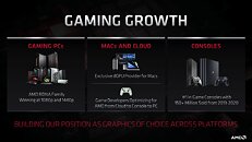
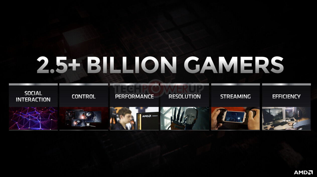
 22:37 UTC: A brief overview of growth in gaming.


22:39 UTC: Brief overview of Navi. Big push for variable-rate-shading (VRS), ray-tracing, and process improvements with RDNA2. AMD's upcoming Navi2X GPUs are described as "Top-of Stack GPUs", "with uncompromising 4K Gaming" — finally some competition for NVIDIA!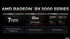
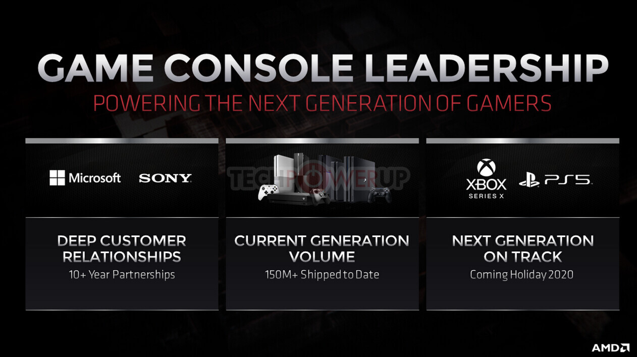
22:43 UTC: AMD chronicles the today and tomorrow of console gaming.
23:09 UTC: Session 2 resumes after a brief recess. Forrest Norrod of Data Center computing takes stage.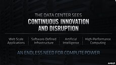
23:14 UTC: If you're impatient about Forrest Norrod's presentation, here are the slides.

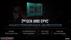


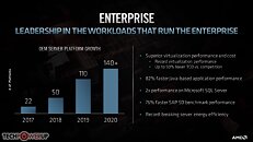
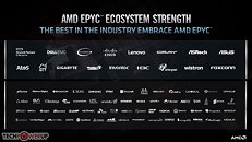
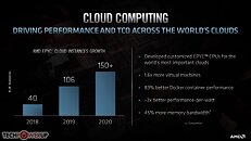

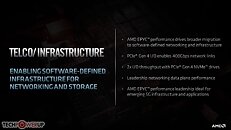
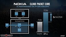
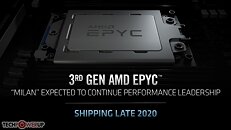
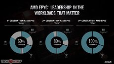


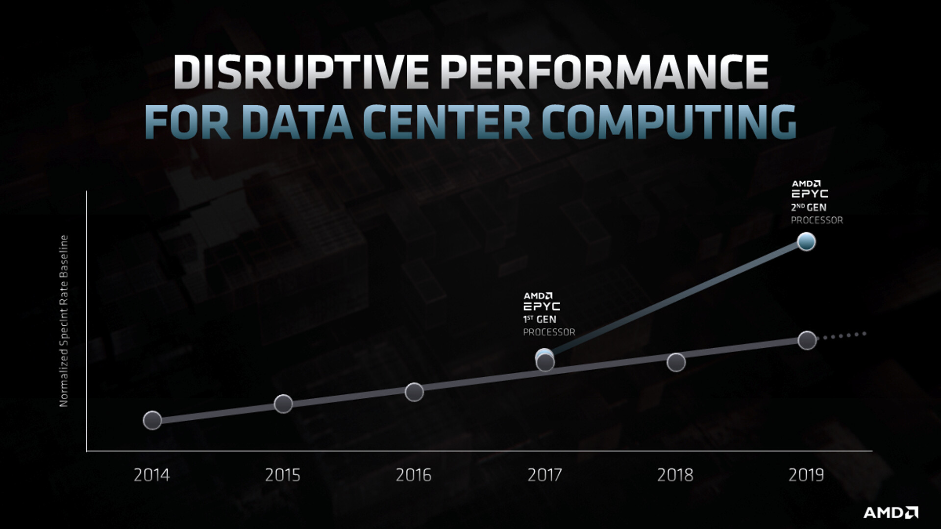
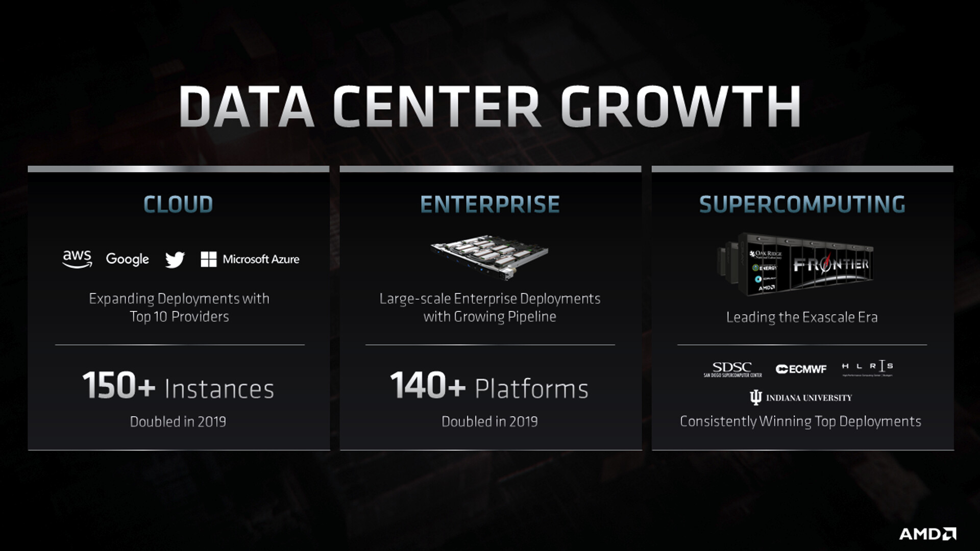
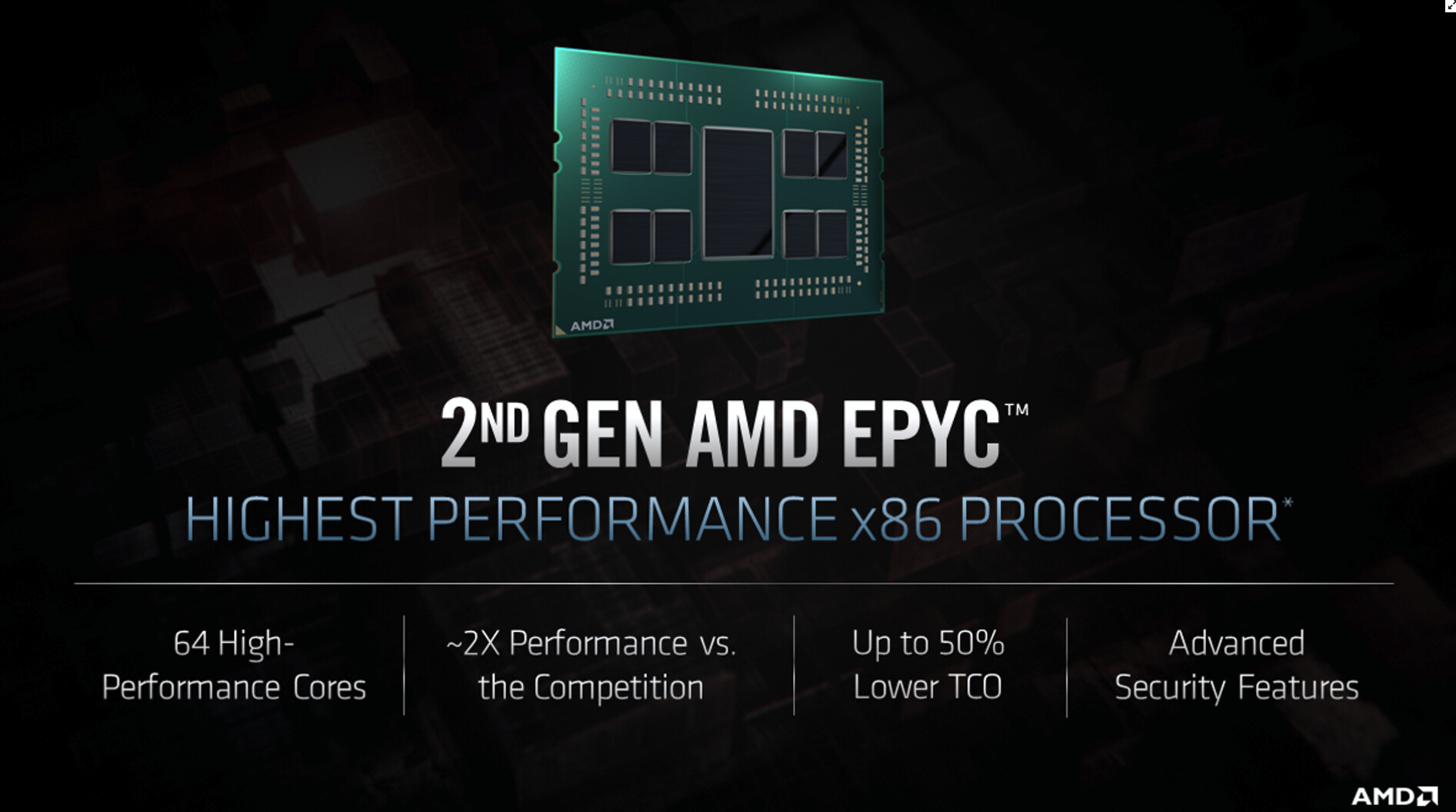
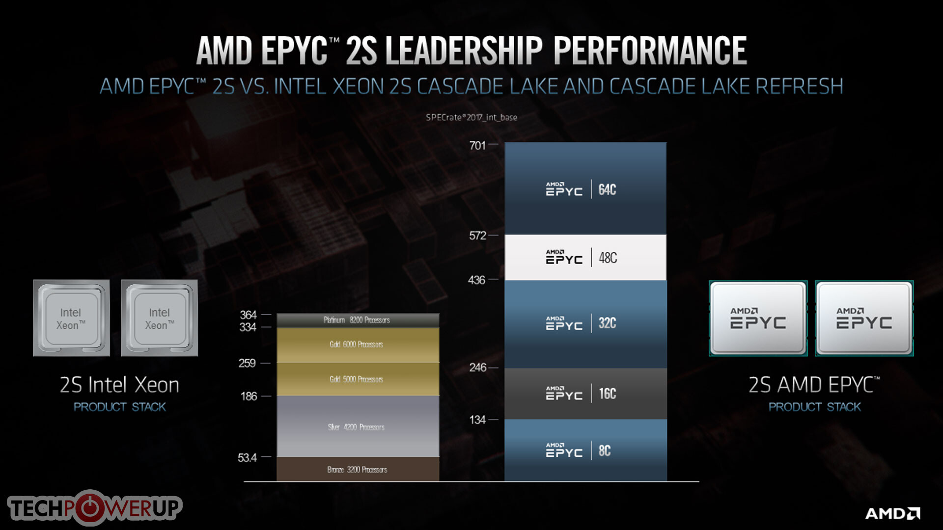
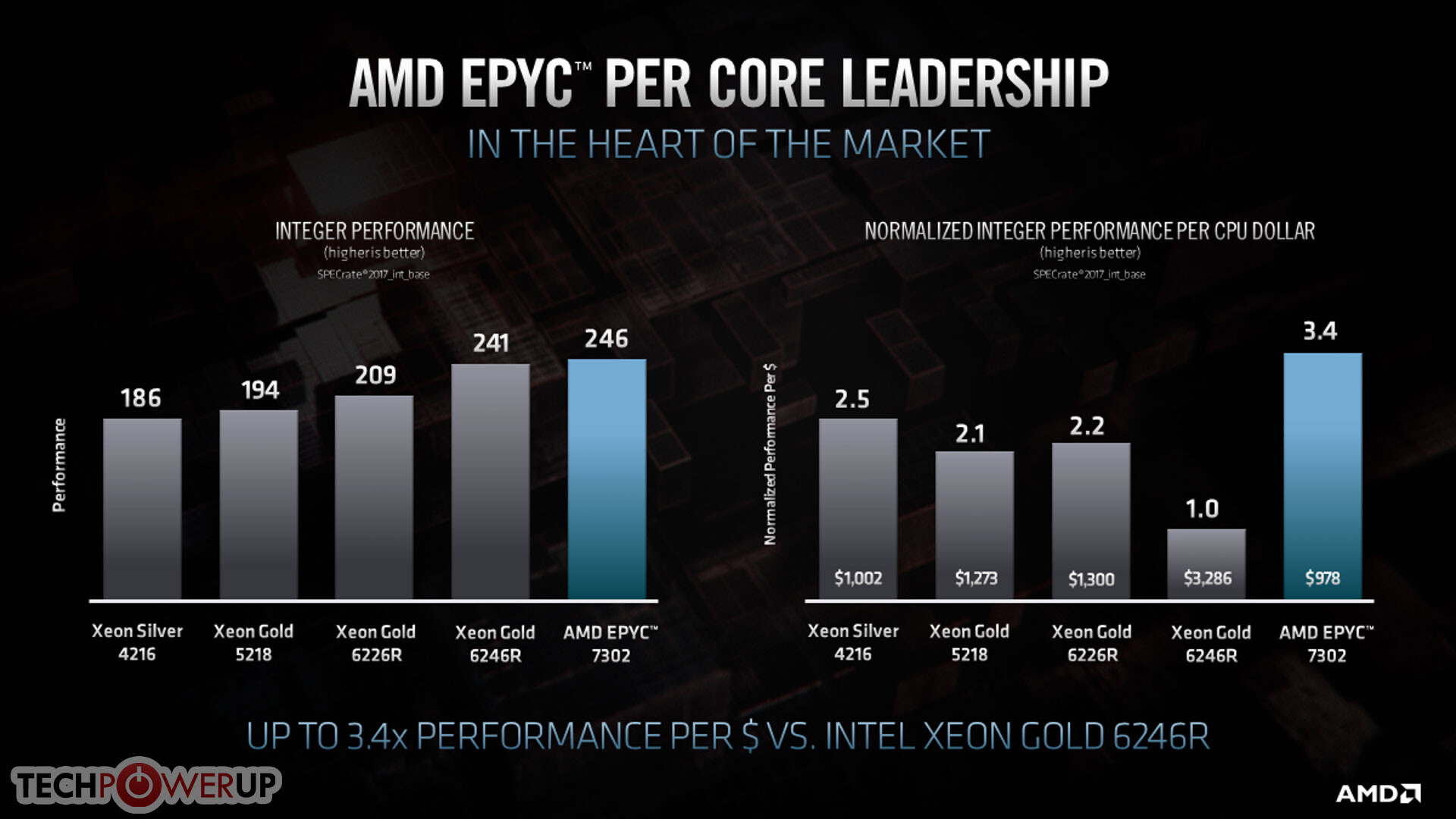
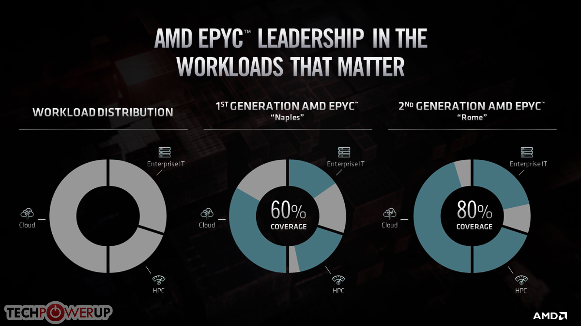
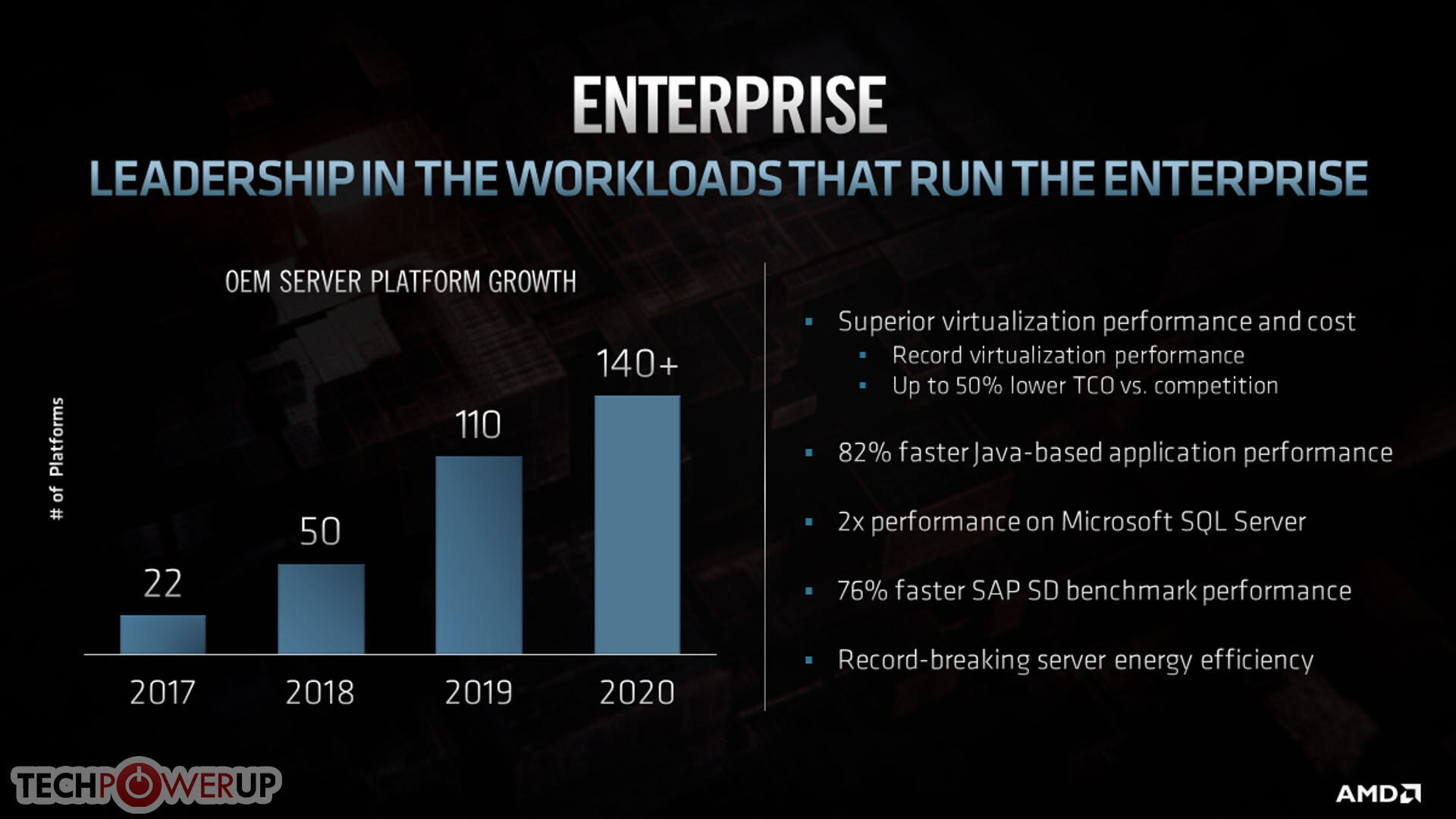
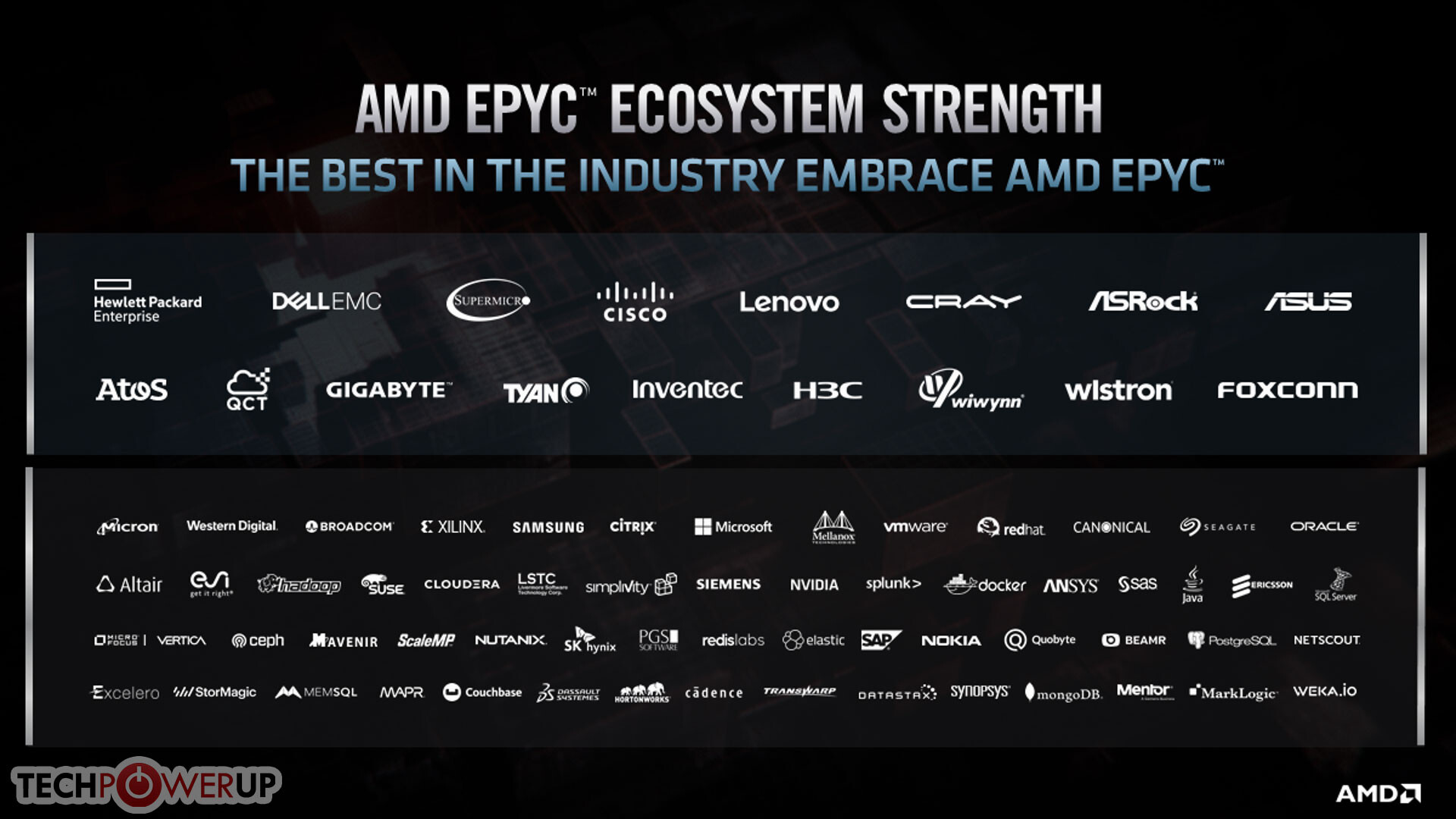
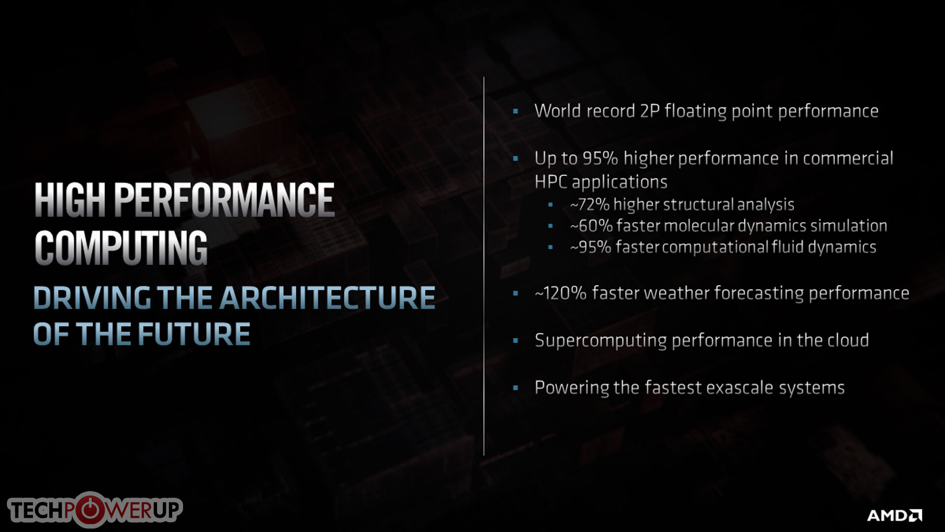
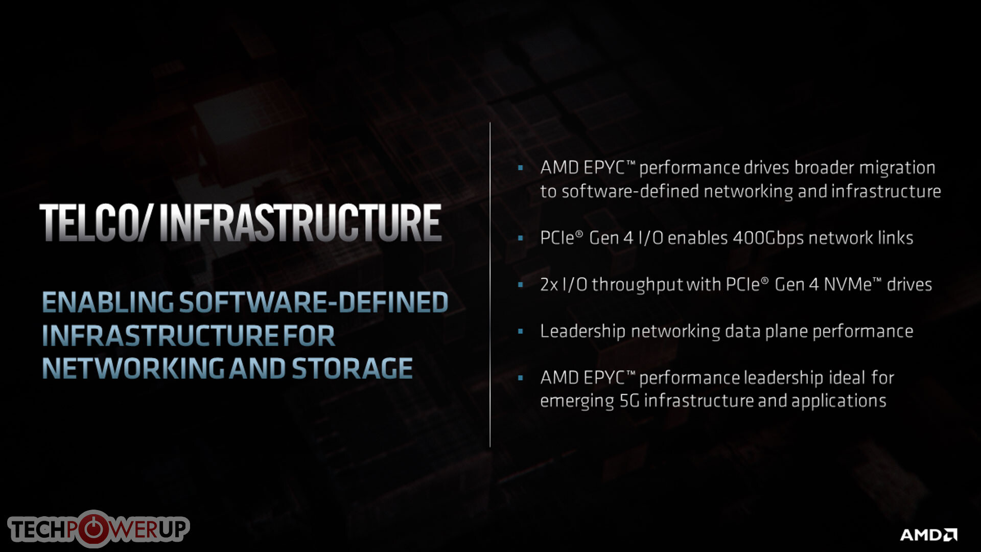
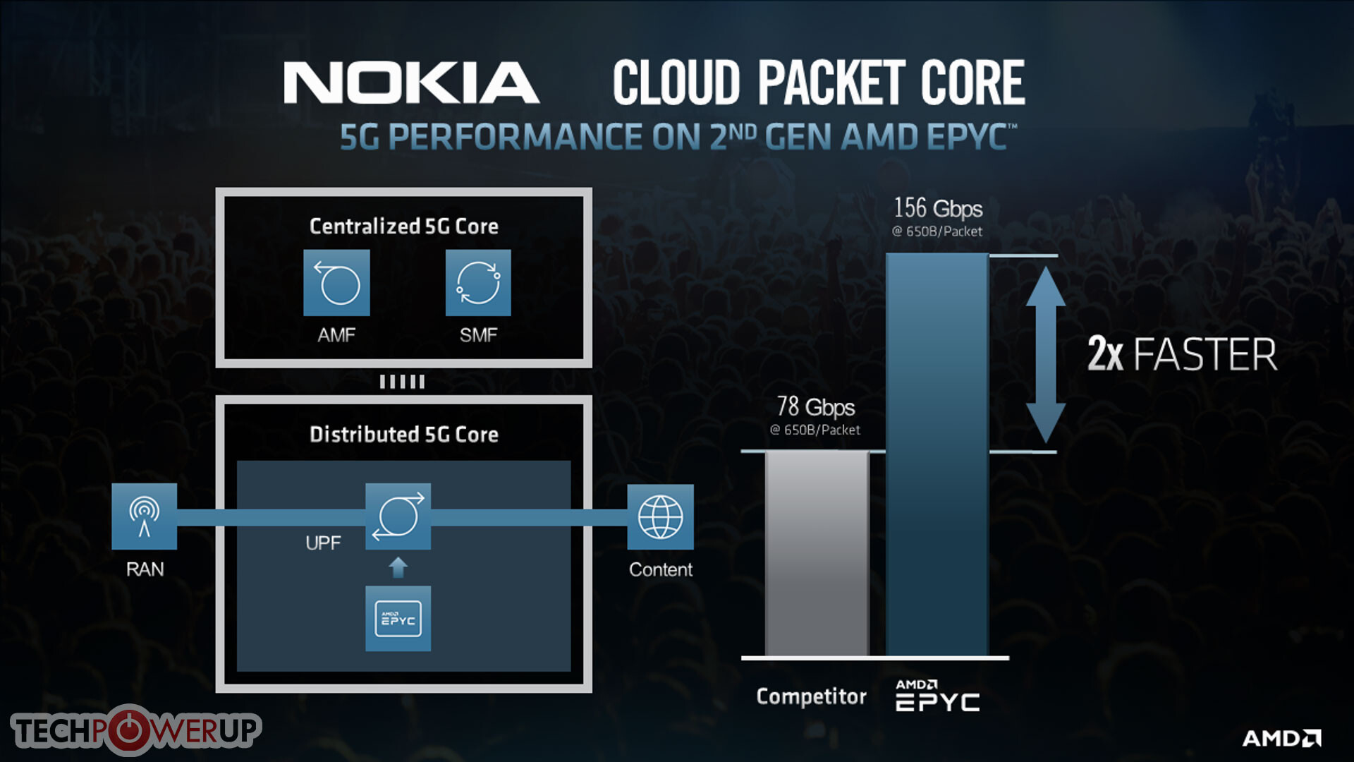
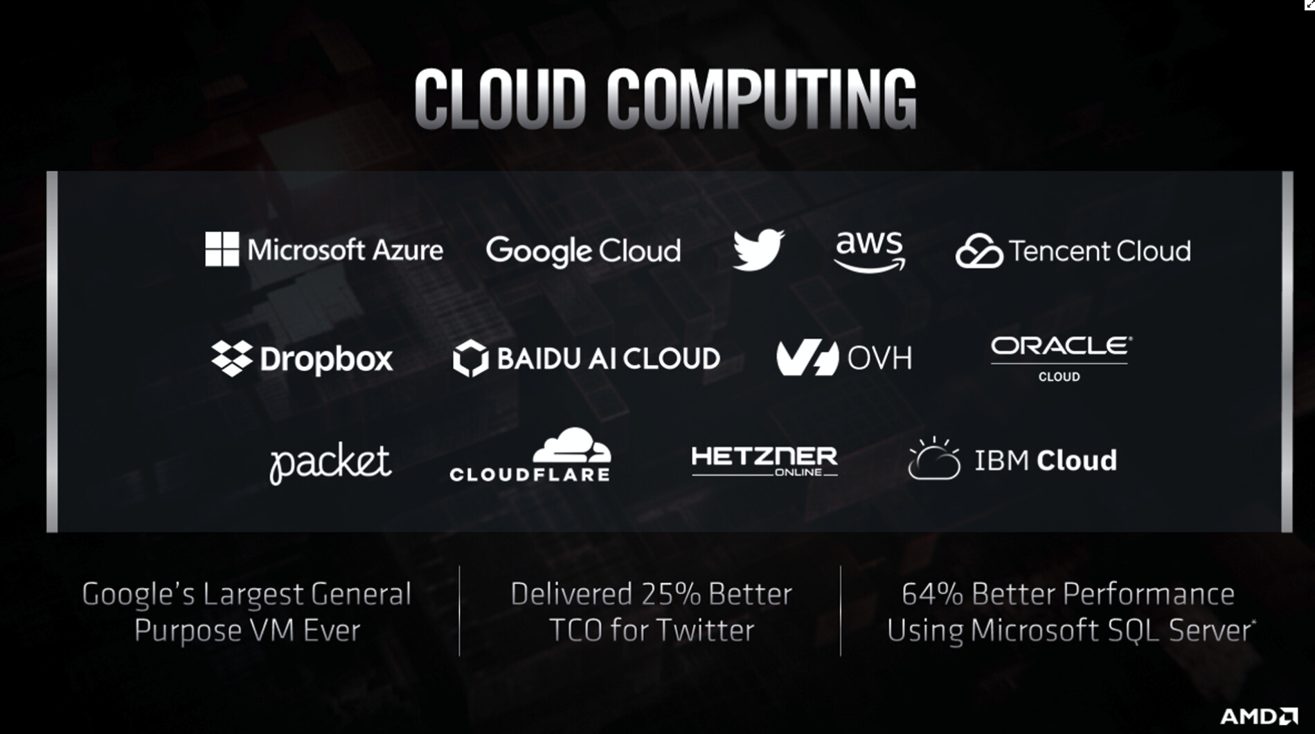
23:20 UTC: Cloud providers love EPYC. The processor is powering Twitter and CloudFlare. 23:24 UTC: HPC is a key technological growth area for AMD on the back of huge design wins. 23:25 UTC: AMD is betting on telecom, particularly the 5G rollout, which has high requirements for IO connectivity — which EPYC is able to provide. 3rd Gen EPYC "Milan" processors will be shipping late-2020.
23:28 UTC: AMD's 4th generation EPYC processors are codenamed "Genoa", and powered by Zen 4 CPU cores. A 5 nm fabrication process is used, coming in 2022.
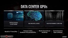
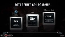
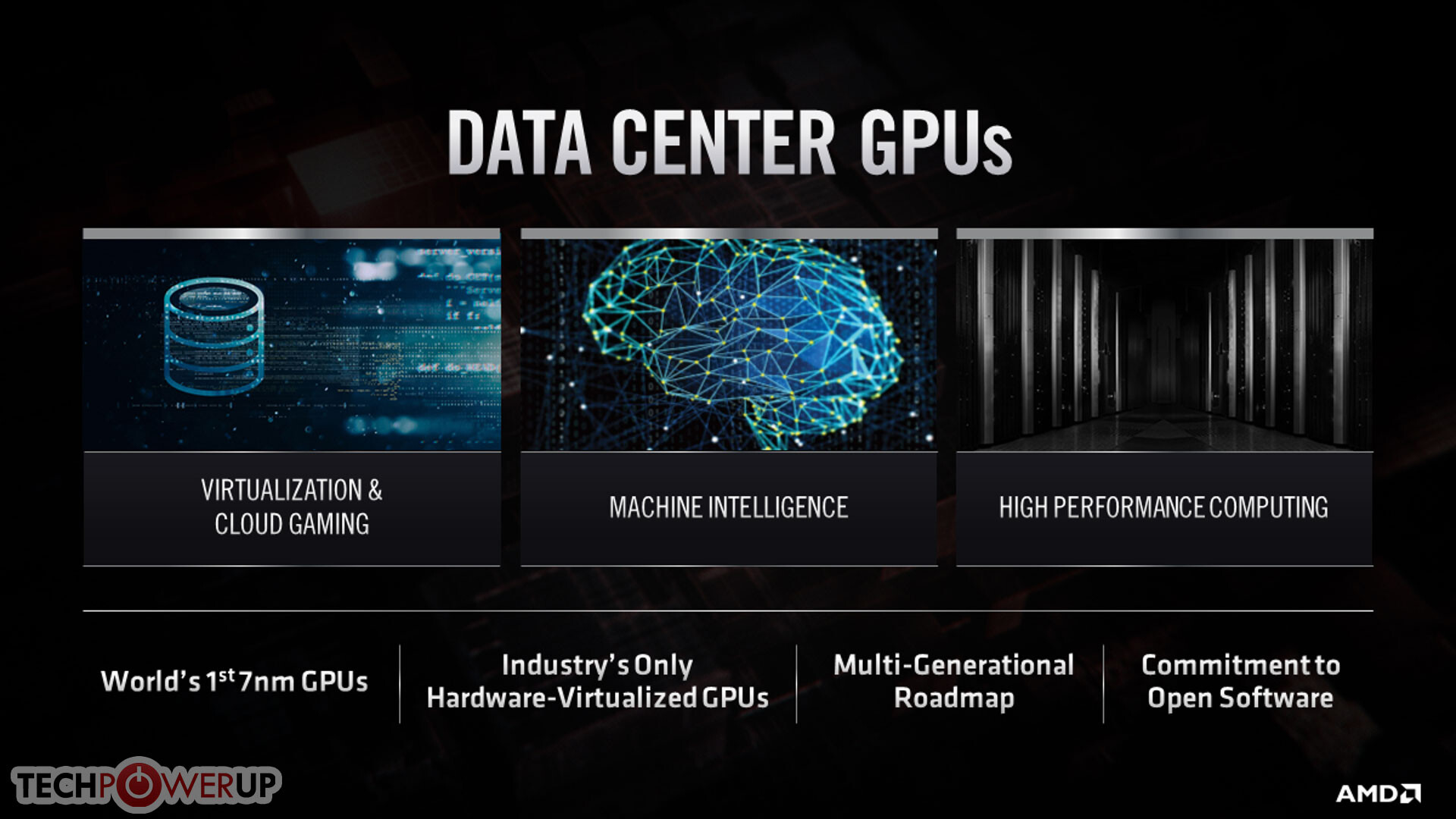
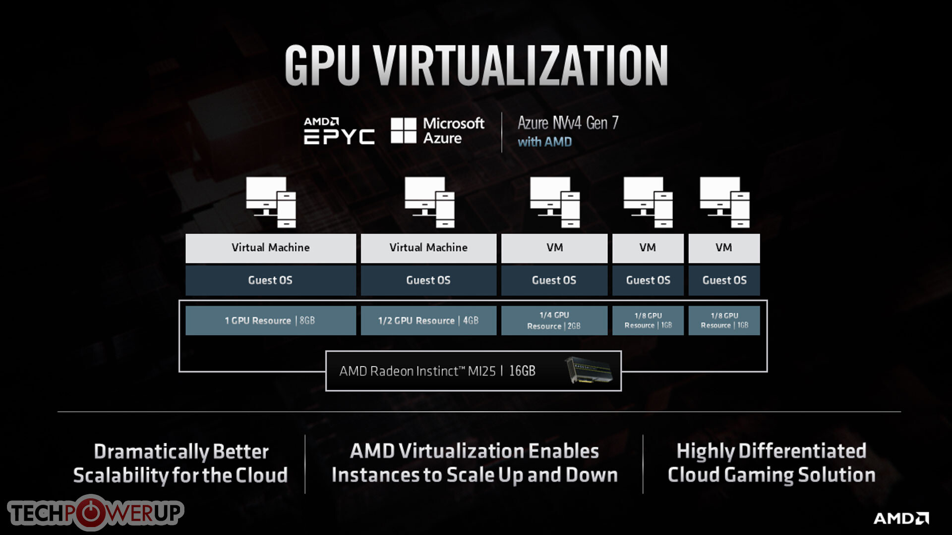
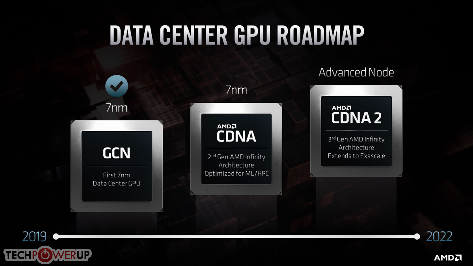
23:30 UTC: Data Center GPUs both for supporting virtual desktops/gaming, and AI/ML a big bet for AMD. 23:34 UTC: Data Centers are handling most of the computing. 10X performance growth needed over the next few years. AMD's Data Center GPU Roadmap shows CDNA, which is optimized for ML/HPC, and CDNA2, which extends the computing capabilities to Exascale. The CDNA2 architecture will also be cache-coherent with the main processor, which means that workloads can live in any memory and don't have to be copied around anymore.
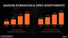
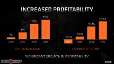
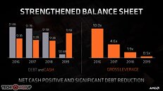
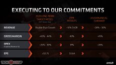
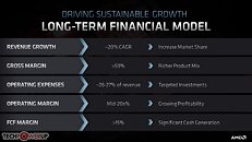
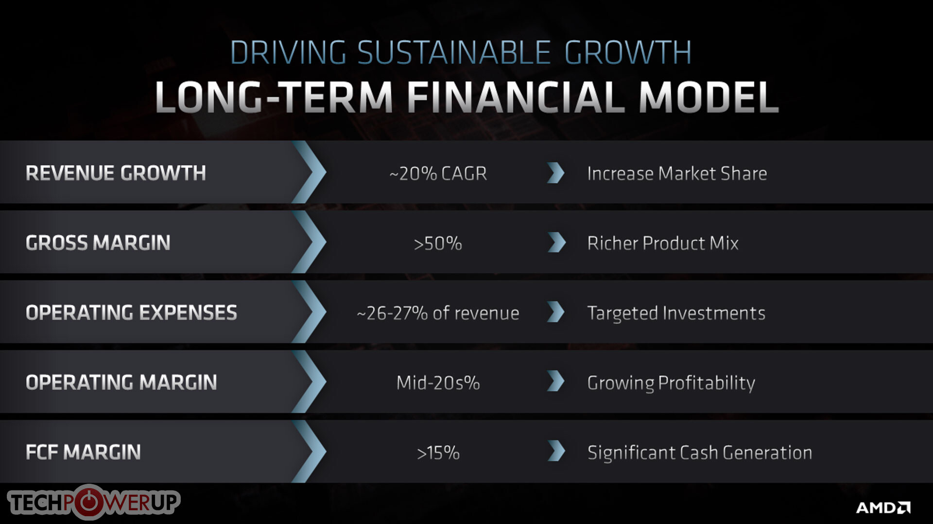
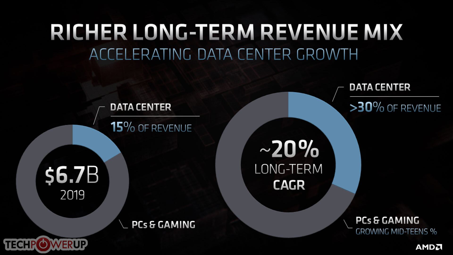
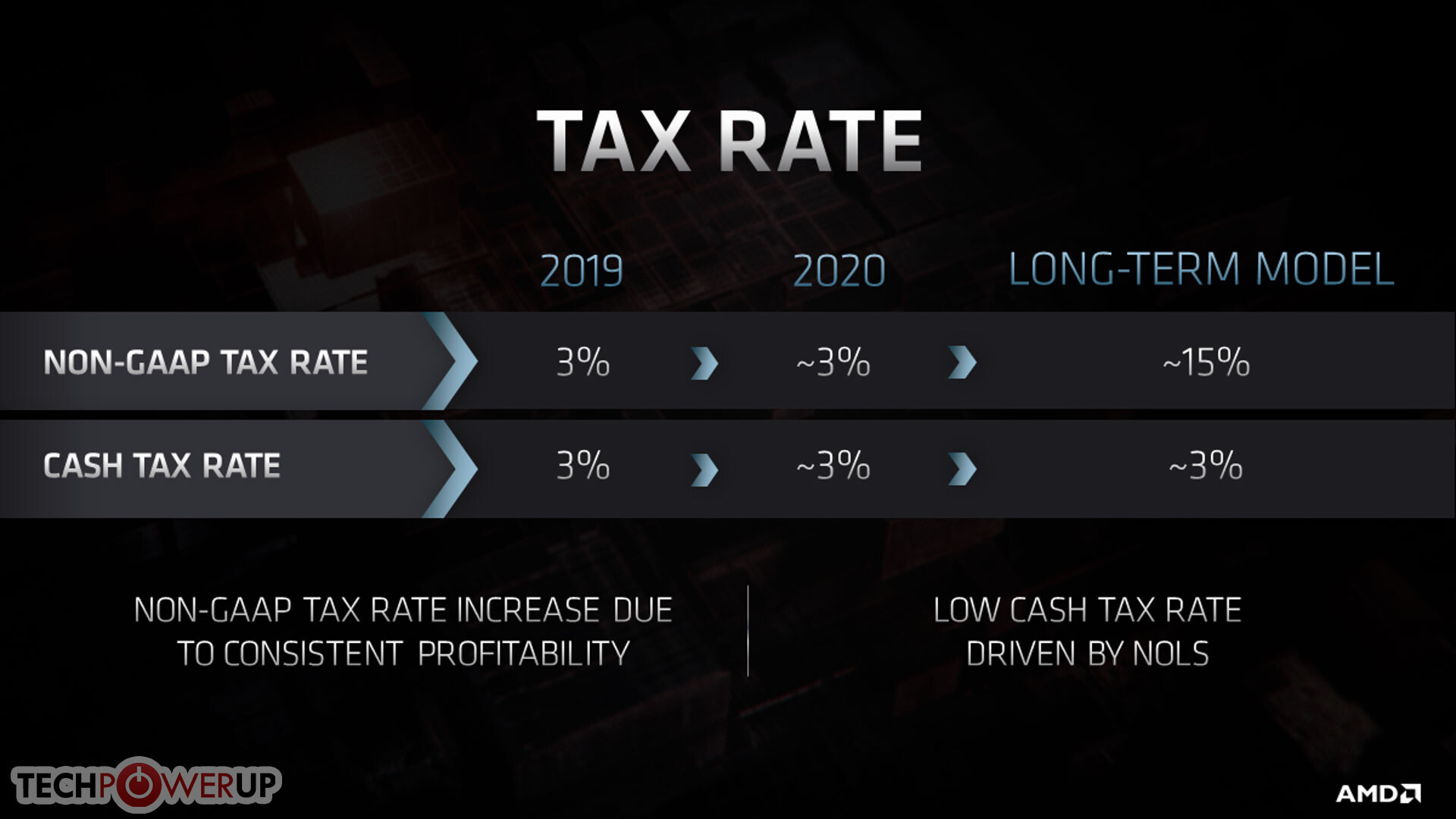
23:41 UTC: Devinder Kumar, CFO takes stage to talk about the company's financials since 2017 and the way forward.
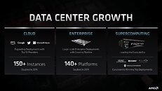
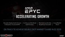
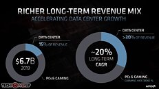
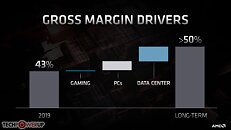
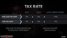
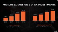 23:43 UTC: Devinder Kumar is presenting AMD financial details now, here's his full slide deck. Data Centers will make up nearly 1/3rd of AMD's revenues in the coming years.


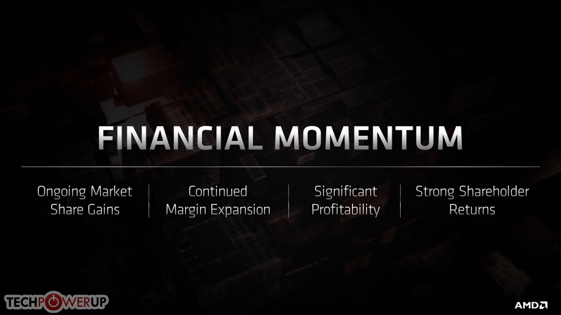
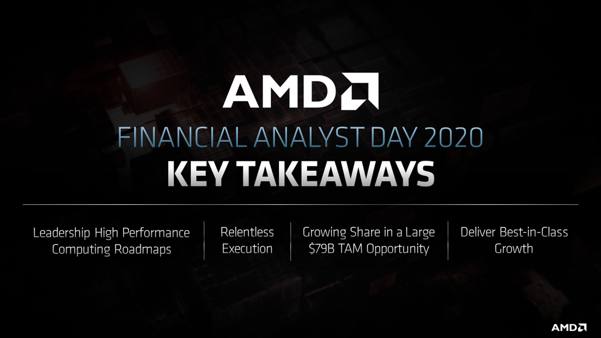
 23:55 UTC: CEO Lisa Su summarizes key takeaways before Q&A.
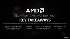
23:58 UTC: CEO Lisa Su talks about the Coronavirus: Protecting employees against COVID-19 at a policy level, supply chains largely unaffected, although partners dependent on China somewhat affected.
Q&A
00:07 UTC: RDNA and CDNA IPC scaling identical.
00:20 UTC: Zen 4 is 5 nm, but AMD is vague on RDNA3 and CDNA2 process. CDNA architecture physically lacks the raster bulk of RDNA, replaced with tensor accelerators (matrix multipliers).
00:31 UTC: And that's a wrap. We will dissect much of the information presented here shortly, into separate news posts.
23 Comments on AMD Financial Analyst Day 2020 Live Blog
All current AMD line ups are works of art. All is well except their gpus and with their excessive voltage regulation. I say release Timothy Lottes and say, "Full power!" to rapid packed math scalarized code in all workloads. They have a good math library compiler now and AMD is specializing in the gpu semi-custom era. Why don't we have optimized low latency code for their gpu titles more often, rapid packed math ought to be the evolution of heterogeneous system architecture.
They didn't want any launch scruples, so the original engine had extra weight for added safety - some 65kg, 301kg total, which got shed in later generations. Likewise, Intel needs a solid footing prior to reinventing the HBM wheel, imo.
...but to stay on topic, I suspect that Intel is working on something. It's not like it's anything they haven't done before if you consider Crystalwell, but they haven't dedicated nearly as many resources into it as AMD has and it's finally paying for (for AMD.) Intel needs to do something to improve yields. They can't play this game forever.
AMD is keeping up with such sound process practices more than anything, don't read between the lines.
www.anandtech.com/show/15589/amd-clarifies-comments-on-7nm-7nm-for-future-products-euv-not-specified
EDIT:
Thank god
While I don't expect AMD to overtake Nvidia in the near future, the comments these days will make you feel RDNA (series) is the dozer to Intel's (Nvidia) Sandy Bridge ~ which is so far away from the truth it's not even funny o_O
I'll paste these here again, for people who have difficulty understanding how efficiency works at different levels & even GPU classes ~
7N+ (EUV) is not.5600, 5700 series "overtook" nvidia.
As for that funny Ti thing for $1.3k, less than one 1% of the market buys them, why should it even matter to the remaining 99%?
Taken from www.techcenturion.com/7nm-10nm-14nm-fabrication
TSMC 7nm vs 12/16nm: 20% performance and 40% power reduction = 60% efficiency
TSMC 7nm+ vs 7nm: 10% performance or 15% power reduction = 15% efficiency
That explains the 75% efficiency increase for you ?
BTW Manufacturer OC cards also increase effiency, it's nothing new
In any case, even if performance per watt improvement is 75%, actual total performance gain is dependant on clockspeeds. I don't think they'll match clockspeeds on their first 7nm products compared to their 12nm cards.
Maxwell to Pascal (similar in architecture)
28nm vs 16nm which TSMC said bring almost 50% more performance and 60% more efficient
980 Ti 250W TDP 6.06 TFLOPS
1080 Ti 250W TDP 11.34 TFLOPS
That is 87% efficiency gain, yeah it's less than 110% promised by TSMC but it's almost. 1080Ti is also 85% faster than 980Ti in 4K benchmark.
Ampere is rumored to be 50% faster than Turing (3080 Ti vs 2080 Ti) at 50% power (most likely testing at reduced power limit), I reckon 3080Ti will end up 75% faster than 2080Ti at 100% power limit (260W TDP). Just recently the Geekbench leaks for Ampere already indicate that anyways.