News Posts matching #Foveros

Return to Keyword Browsing

Intel Lunar Lake Chiplet Arrangement Sees Fewer Tiles—Compute and SoC

Intel Core Ultra "Lunar Lake-MX" will be the company's bulwark against Apple's M-series Pro and Max chips, designed to power the next crop of performance ultraportables. The MX codename extension denotes MoP (memory-on-package), which sees stacked LPDDR5X memory chips share the package's fiberglass substrate with the chip, to conserve PCB footprint, and give Intel greater control over the right kind of memory speed, timings, and power-management features suited to its microarchitecture. This is essentially what Apple does with its M-series SoCs powering its MacBooks and iPad Pros. Igor's Lab scored the motherlode on the way Intel has restructured the various components across its chiplets, and the various I/O wired to the package.

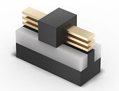
When compared to "Meteor Lake," the "Lunar Lake" microarchitecture sees a small amount of "re-aggregation" of the various logic-heavy components of the processor. On "Meteor Lake," the CPU cores and the iGPU sat on separate tiles—Compute tile and Graphics tile, respectively, with a large SoC tile sitting between them, and a smaller I/O tile that serves as an extension of the SoC tile. All four tiles sat on top of a Foveros base tile, which is essentially an interposer—a silicon die that facilitates high-density microscopic wiring between the various tiles that are placed on top of it. With "Lunar Lake," there are only two tiles—the Compute tile, and the SoC tile.

Intel Redefines the Foundry for an Era of AI

Artificial intelligence isn't just driving headlines and stock valuations. It's also "pushing the boundaries of silicon technology, packaging technology, the construction of silicon, and the construction of racks and data centers," says Intel's Bob Brennan. "There is an insatiable demand," Brennan adds. Which is great timing since his job is to help satisfy that demand.

Brennan leads customer solutions engineering for Intel Foundry, which aims to make it as easy and fast as possible for the world's fabless chipmakers to fabricate and assemble their chips through Intel factories. "We are engaged from architecture to high-volume manufacturing—soup to nuts—and we present the customer with a complete solution," Brennan asserts.

US Government to Announce Massive Grant for Intel's Arizona Facility

According to the latest report by Reuters, the US government is preparing to announce a multi-billion dollar grant for Intel's chip manufacturing operations in Arizona next week, possibly worth more than $10 billion. US President Joe Biden and Commerce Secretary Gina Raimondo will make the announcement, which is part of the 2022 CHIPS and Science Act aimed at expanding US chip production and reducing dependence on China and Taiwan manufacturing. The exact amount of the grant has yet to be confirmed, but rumors suggest it could exceed $10 billion, making it the most significant award yet under the CHIPS Act. The funding will include grants and loans to bolster Intel's competitive position and support the company's US semiconductor manufacturing expansion plans. This comes as a surprise just a day after the Pentagon reportedly refused to invest $2.5 billion in Intel as a part of a secret defense grant.

Intel has been investing significantly in its US expansion, recently opening a $3.5 billion advanced packaging facility in New Mexico, supposed to create extravagant packaging technology like Foveros and EMIB. The chipmaker is also expanding its semiconductor manufacturing capacity in Arizona, with plans to build new fabs in the state. Arizona is quickly becoming a significant hub for semiconductor manufacturing in the United States. In addition to Intel's expansion, Taiwan Semiconductor Manufacturing Company (TSMC) is also building new fabs in the state, attracting supply partners to the region. CHIPS Act has a total funding capacity of $39 billion allocated for semiconductor production and $11 billion for research and development. The Intel grant will likely cover the production part, as Team Blue has been reshaping its business units with the Intel Product and Intel Foundry segments.

Intel "Lunar Lake-U" 17W Processor Offers Almost 50% Multithreaded Perf Boost Over "Meteor Lake" 15W Despite Lack of HTT

There is some confidence behind removing HTT (Hyper-Threading technology) for the P-cores of its upcoming processor generations. Apparently "Lunar Lake" 17 W U-segment processors offer a substantial multithreaded performance gain of almost 50% over the current-generation "Meteor Lake," enabling Intel to do away with the power- or cache overheads that come with HTT. "Lunar Lake" will be Intel's third microarchitecture powering mobile processors under the Core Ultra brand; and its U-segment SKUs meant for ultraportables will come with processor base power values of 17 W. Intel will probably revise its platform specifications for the U-segment to denote 17 W, up from the current 15 W. Bionic Squash, a reliable source with Intel leaks, suggests so. The processors will come with a configurable base power of up to 30 W.

Intel "Lunar Lake" microarchitecture has a lot in common with the upcoming "Arrow Lake." For starters, both microarchitectures use the same combination of "Lion Cove" P-core architecture, and "Skymont" E-core architecture; however "Lunar Lake" comes with changes in the core-configuration, and the use of more advanced foundry nodes for some of its tiles. "Lunar Lake," much like "Meteor Lake," comes with a design priority for mobile platforms, which is why Intel is planning to launch this shortly after "Arrow Lake," with some reports even speaking of a late-2024 debut for the U-segment.

Intel to Tease Core Ultra "Arrow Lake" at Computex?

Intel is rumored to be preparing to tease its Core Ultra 2-series "Arrow Lake" processor at the 2024 Computex, which gets underway this June. The series itself isn't expected to launch before Q4-2024, but Computex is the only major global event between June and January for Intel to unveil or tease its next-generation processor, so here we are. At this point we don't know which exact platform of "Arrow Lake" Intel is planning to tease—whether these are the mobile variants, or the Socket LGA1851 desktop "Arrow Lake-S." An unveiling of the latter would almost definitely entail PC motherboard vendors being allowed to show off their first compatible motherboards at Computex—the perfect platform for them to do so.

The Core Ultra "Arrow Lake" retains a Foveros Tiled (chiplet) construction of "Meteor Lake," but with advancements to the chip's Compute tile, which is built on the Intel 20A foundry node, and rocks new "Lion Cove" P-cores and "Skymont" E-cores; an updated I/O tile, and an iGPU based on the updated Xe-LPG+ graphics architecture. Since the processor now serves practically all PCH functions, the mobile "Arrow Lake" is a single-chip solution, whereas the desktop "Arrow Lake-S" is expected to remain 2-chip. There will be more I/O from the CPU, though, which is why the socket has 151 more pins than the LGA1700.

Intel to Make its Most Advanced Foundry Nodes Available even to AMD, NVIDIA, and Qualcomm

Intel CEO Pat Gelsinger, speaking at the Intel Foundry Services (IFS) Direct Connect event, confirmed to Tom's Hardware that he hopes to turn IFS into the West's premier foundry company, and a direct technological and volume rival to TSMC. He said that there is a clear line of distinction between Intel Products and Intel Foundry, and that later this year, IFS will be more legally distinct from Intel, becoming its own entity. The only way Gelsinger sees IFS being competitive to TSMC, is by making its most advanced semiconductor manufacturing nodes and 3D chip packaging innovations available to foundry customers other than itself (Intel Products), even if it means providing them to companies that directly compete with Intel products, such as AMD and Qualcomm.

Paul Alcorn of Tom's Hardware asked CEO Gelsinger "Intel will now offer its process nodes to some of its competitors, and there may be situations wherein your product teams are competing directly with competitors that are enabled by your crown jewels. How do you plan to navigate those types of situations and maybe soothe ruffled feathers on your product teams?" To this, Gelsinger responded "Well, if you go back to the picture I showed today, Paul, there are Intel products and Intel foundry, There's a clean line between those, and as I said on the last earnings call, we'll have a setup separate legal entity for Intel foundry this year," Gelsinger responded. "We'll start posting separate financials associated with that going forward. And the foundry team's objective is simple: Fill. The. Fabs. Deliver to the broadest set of customers on the planet."

Intel Lunar Lake-MX to Embed Samsung LPDDR5X Memory on SoC Package

According to sources close to Seoul Economy, and reported by DigiTimes, Intel has reportedly chosen Samsung as a supplier for its next-generation Lunar Lake processors, set to debut later this year. The report notes that Samsung will provide LPDDR5X memory devices for integration into Intel's processors. This collaboration could be a substantial win for Samsung, given Intel's projection to distribute millions of Lunar Lake CPUs in the coming years. However, it's important to note that this information is based on a leak and has not been officially confirmed. Designed for ultra-portable laptops, the Lunar Lake-MX platform is expected to feature 16 GB or 32 GB of LPDDR5X-8533 memory directly on the processor package. This on-package memory approach aims to minimize the platform's physical size while enhancing performance over traditional memory configurations. With Lunar Lake's exclusive support for on-package memory, Samsung's LPDDR5X-8533 products could significantly boost sales.

While Samsung is currently in the spotlight, it remains unclear if it will be the sole LPDDR5X memory provider for Lunar Lake. Intel's strategy involves selling processors with pre-validated memory, leaving the door open for potential validation of similar memory products from competitors like Micron and SK Hynix. Thanks to a new microarchitecture, Intel has promoted its Lunar Lake processors as a revolutionary leap in performance-per-watt efficiency. The processors are expected to utilize a multi-chipset design with Foveros technology, combining CPU and GPU chipsets, a system-on-chip tile, and dual memory packages. The CPU component is anticipated to include up to eight cores, a mix of four high-performance Lion Cove and four energy-efficient Skymont cores, alongside advanced graphics, cache, and AI acceleration capabilities. Apple's use of on-package memory in its M-series chips has set a precedent in the industry, and with Intel's Lunar Lake MX, this trend could extend across the thin-and-light laptop market. However, systems requiring more flexibility in terms of configuration, repair, and upgrades will likely continue to employ standard memory solutions like SODIMMs and/or the new CAMM2 modules that offer a balance of high performance and energy efficiency.

Intel Opens Fab 9 Foundry in New Mexico

Today, Intel celebrated the opening of Fab 9, its cutting-edge factory in Rio Rancho, New Mexico. The milestone is part of Intel's previously announced $3.5 billion investment to equip its New Mexico operations for the manufacturing of advanced semiconductor packaging technologies, including Intel's breakthrough 3D packaging technology, Foveros, which offers flexible options for combining multiple chips that are optimized for power, performance and cost.

"Today, we celebrate the opening of Intel's first high-volume semiconductor operations and the only U.S. factory producing the world's most advanced packaging solutions at scale. This cutting-edge technology sets Intel apart and gives our customers real advantages in performance, form factor and flexibility in design applications, all within a resilient supply chain. Congratulations to the New Mexico team, the entire Intel family, our suppliers, and contractor partners who collaborate and relentlessly push the boundaries of packaging innovation," said Keyvan Esfarjani, Intel executive vice president and chief global operations officer.

Intel Unveils "Arrow Lake" for Desktops, "Lunar Lake" for Mobile, Coming This Year

Intel in its 2024 International CES presentation, unveiled its two new upcoming client microarchitectures, "Arrow Lake" and "Lunar Lake." Michelle Johnston Holthaus, EVP and GM of Intel's client computing group (CCG), in her keynote address, held up a next-generation Core Ultra "Lunar Lake" chip. This is the Lunar Lake-MX package, with MOP (memory on package). You have a Foveros base tile resembling "Meteor Lake," with on-package LPDDR5x memory stacks. With "Lunar Lake," Intel is reorganizing components across its various Foveros tiles—the Compute and Graphics tiles are combined into a single tile built on an Intel foundry node that's possibly the Intel 20A (we have no confirmation); and a smaller SoC tile that has all of the components of the current "Meteor Lake" SoC tile, and is possibly built on a TSMC node, such as N3.

"Lunar Lake" will pick up the mantle from "Meteor Lake" in the U-segment and H-segment (that's ultraportables, and thin-and-light), when it comes out later this year (we predict in the second half of 2024), with Core Ultra 2-series branding. Intel also referenced "Arrow Lake," which could finally bring light to the sluggish pace of development in its desktop segment. When it comes out later this year, "Arrow Lake" will debut Socket LGA1851, "Arrow Lake" will bring the AI Boost NPU to the desktop, along with Arc Xe-LPG integrated graphics. The biggest upgrade of course will be its new Compute tile, with its "Lion Cove" P-cores, and "Skymont" E-cores, that possibly offer a large IPC uplift over the current combination of "Raptor Cove" and "Gracemont" cores on the "Raptor Lake" silicon. It's also possible that Intel will try to bring "Meteor Lake" with its 6P+8E Compute tile, Xe-LPG iGPU, and NPU, to the LGA1851 socket, as part of some mid-range processor models. 2024 will see a Intel desktop processor based on a new architecture, which is the big takeaway here.

Intel Core Ultra "Meteor Lake" Processor Lineup Overview

On December 14 Intel launched its first generation Core Ultra "Meteor Lake" line of mobile processors, and here is a a brief overview of the various processor models on offer at launch, thanks to a compilation by ComputerBase.de. "Meteor Lake" is Intel's first completely disaggregated processor, in which its numerous components are broken up into chiplets fabricated on different foundry nodes that strike the right performance/Watt suitable to the component, all held together by Intel's Foveros packaging technology (an evolution in multi-chip modules with a design focus on reducing inter-chiplet latencies to levels comparable to components on a monolithic chip). "Meteor Lake" also introduces a 3-tiered heterogeneous CPU architecture, with the introduction of the low-power island CPU cores.

Intel's mobile processor lineup is broadly categorized into the U-segment, targeting thin-and-light and ultraportable devices; and the H-segment, targeting notebooks of conventional thickness. At launch, the Core Ultra H-segment, and U-segment processors will coexist with P-segment processor models from the 13th Gen Core "Raptor Lake" series; as well as the upcoming 14th Gen Core "Raptor Lake Refresh" HX-segment. The P-segment is positioned between the U- and H-segments, targeting a class of devices that either what to be thin-and-light mainstream notebooks, or higher performance ultraportables. The HX-segment caters to high performance gaming notebooks and mobile workstations.

Intel Lunar Lake-MX SoC with On-Package LPDDR5X Memory Detailed

With the reality of high performance Arm processors from Apple and Qualcomm threatening Intel's market share in the client computing space, Intel is working on learner more PCB-efficient client SoCs that can take the fight to them, while holding onto the foundations of x86. The first such form-factor of processors are dubbed -MX. These are essentially -U segment processors with memory on package, to minimize PCB footprint. Intel has fully integrated the PCH into the processor chip with "Meteor Lake," with PCH functions scattered across the SoC and I/O tiles of the processor. An SoC package with dimensions similar to those of -UP4 packages meant for ultrabooks, can now cram main memory, so the PCBs of next-generation notebooks can be further compacted.

Intel had recently shown Meteor Lake-MX packages to the press as a packaging technology demonstration in its Arizona facility. It's unclear whether this could release as actual products, but in a leaked company presentation, confirmed that its first commercial outing will be with Lunar Lake-MX. The current "Alder Lake-UP4" package measures 19 mm x 28.5 mm, and is a classic multi-chip module that combines a monolithic "Alder Lake" SoC die with a PCH die. The "Meteor Lake-UP4" package measures 19 mm x 23 mm, and is a chiplet-based processor, with a Foveros base tile that holds the Compute (CPU cores), Graphics (iGPU), SoC and I/O (platform core-logic) tiles. The "Lunar Lake-MX" package is slightly larger than its -UP4 predecessors, measuring 27 mm x 27.5 mm, but completely frees up space on the PCB for memory.

Intel Innovation 2023: Bringing AI Everywhere

As the world experiences a generational shift to artificial intelligence, each of us is participating in a new era of global expansion enabled by silicon. It's the "Siliconomy," where systems powered by AI are imbued with autonomy and agency, assisting us across both knowledge-based and physical-based tasks as part of our everyday environments.

At Intel Innovation, the company unveiled technologies to bring AI everywhere and to make it more accessible across all workloads - from client and edge to network and cloud. These include easy access to AI solutions in the cloud, better price performance for Intel data center AI accelerators than the competition offers, tens of millions of new AI-enabled Intel PCs shipping in 2024 and tools for securely powering AI deployments at the edge.

Intel's Meteor Lake CPU Breaks Ground with On-Package LPDDR5X Memory Integration

During a recent demonstration, Intel showcased its cutting-edge packaging technologies, EMIB (embedded multi-die interconnect bridge) and Foveros, unveiling the highly-anticipated Meteor Lake processor with integrated LPDDR5X memory. This move appears to align with Apple's successful integration of LPDDR memory into its M1 and M2 chip packages. At the heart of Intel's presentation was the quad-tile Meteor Lake CPU, leveraging Foveros packaging for its chiplets and boasting 16 GB of Samsung's LPDDR5X-7500 memory. Although the specific CPU configuration remains undisclosed, the 16 GB of integrated memory delivers a remarkable peak bandwidth of 120 GB/s, outperforming traditional memory subsystems using DDR5-5200 or LPDDR5-6400.

Nevertheless, this approach comes with trade-offs, such as the potential for system-wide failure if a memory chip malfunctions, limited upgradeability in soldered-down configurations, and the need for more advanced cooling solutions to manage CPU and memory heat. While Apple pioneered on-package LPDDR memory integration in client CPUs, Intel has a history of using package-on-package DRAM with its Atom-branded CPUs for tablets and ultrathin laptops. While this approach simplifies manufacturing, enabling slimmer notebook designs, it curtails configuration flexibility. We are yet to see if big laptop makers such as Dell, HP, and Asus, take on this design in the coming months.

Intel Research Fuels Moore's Law and Paves the Way to a Trillion Transistors by 2030

Today, Intel unveiled research breakthroughs fueling its innovation pipeline for keeping Moore's Law on track to a trillion transistors on a package in the next decade. At IEEE International Electron Devices Meeting (IEDM) 2022, Intel researchers showcased advancements in 3D packaging technology with a new 10x improvement in density; novel materials for 2D transistor scaling beyond RibbonFET, including super-thin material just 3 atoms thick; new possibilities in energy efficiency and memory for higher-performing computing; and advancements for quantum computing.

"Seventy-five years since the invention of the transistor, innovation driving Moore's Law continues to address the world's exponentially increasing demand for computing. At IEDM 2022, Intel is showcasing both the forward-thinking and concrete research advancements needed to break through current and future barriers, deliver to this insatiable demand, and keep Moore's Law alive and well for years to come." -Gary Patton, Intel vice president and general manager of Components Research and Design Enablement

Intel to Present Meteor/Arrow Lake with Foveros 3D Packaging at Hot Chips 34

Hot Chips 34, the upcoming semiconductor conference from Sunday, August 21 to Tuesday, August 23, 2022, will feature many significant contributions from folks like Intel, AMD, Tesla, and NVIDIA. Today, thanks to Intel's registration at the event, we discovered that the company would present its work on Meteor Lake and Arrow Lake processors with the novel Foveros 3D packaging. The all-virtual presentation from Intel will include talks about Ponte Vecchio GPU and its architecture, system, and software; Meteorlake and Arrowlake 3D Client Architecture Platform with Foveros; and some Xeon D and FPGA presentations. You can see the official website here for a complete list of upcoming talks.

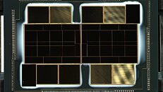
As a little reminder, Meteor Lake is supposed to arrive next year, replacing the upcoming Raptor Lake design, and it has already ahs been pictured, which you can see below. The presentation will be recorded and all content posted on Hot Chips's website for non-attendees to catch up on.

Intel Details Ponte Vecchio Accelerator: 63 Tiles, 600 Watt TDP, and Lots of Bandwidth

During the International Solid-State Circuits Conference (ISSCC) 2022, Intel gave us a more significant look at its upcoming Ponte Vecchio HPC accelerator and how it operates. So far, Intel convinced us that the company created Ponte Vecchio out of 47 tiles glued together in one package. However, the ISSCC presentation shows that the accelerator is structured rather interestingly. There are 63 tiles in total, where 16 are reserved for compute, eight are used for RAMBO cache, two are Foveros base tiles, two represent Xe-Link tiles, eight are HBM2E tiles, and EMIB connection takes up 11 tiles. This totals for about 47 tiles. However, an additional 16 thermal tiles used in Ponte Vecchio regulate the massive TDP output of this accelerator.

What is interesting is that Intel gave away details of the RAMBO cache. This novel SRAM technology uses four banks of 3.75 MB groups total of 15 MB per tile. They are connected to the fabric at 1.3 TB/s connection per chip. In contrast, compute tiles are connected at 2.6 TB/s speeds to the chip fabric. With eight RAMBO cache tiles, we get an additional 120 MB SRAM present. The base tile is a 646 mm² die manufactured in Intel 7 semiconductor process and contains 17 layers. It includes a memory controller, the Fully Integrated Voltage Regulators (FIVR), power management, 16-lane PCIe 5.0 connection, and CXL interface. The entire area of Ponte Vecchio is rather impressive, as 47 active tiles take up 2,330 mm², whereas when we include thermal dies, the total area jumps to 3,100 mm². And, of course, the entire package is much larger at 4,844 mm², connected to the system with 4,468 pins.

Intel Updates Technology Roadmap with Data Center Processors and Game Streaming Service

At Intel's 2022 Investor Meeting, Chief Executive Officer Pat Gelsinger and Intel's business leaders outlined key elements of the company's strategy and path for long-term growth. Intel's long-term plans will capitalize on transformative growth during an era of unprecedented demand for semiconductors. Among the presentations, Intel announced product roadmaps across its major business units and key execution milestones, including: Accelerated Computing Systems and Graphics, Intel Foundry Services, Software and Advanced Technology, Network and Edge, Technology Development, More: For more from Intel's Investor Meeting 2022, including the presentations and news, please visit the Intel Newsroom and Intel.com's Investor Meeting site.

Intel Breakthroughs Propel Moore's Law Beyond 2025

In its relentless pursuit of Moore's Law, Intel is unveiling key packaging, transistor and quantum physics breakthroughs fundamental to advancing and accelerating computing well into the next decade. At IEEE International Electron Devices Meeting (IEDM) 2021, Intel outlined its path toward more than 10x interconnect density improvement in packaging with hybrid bonding, 30% to 50% area improvement in transistor scaling, major breakthroughs in new power and memory technologies, and new concepts in physics that may one day revolutionize computing.

"At Intel, the research and innovation necessary for advancing Moore's Law never stops. Our Components Research Group is sharing key research breakthroughs at IEDM 2021 in bringing revolutionary process and packaging technologies to meet the insatiable demand for powerful computing that our industry and society depend on. This is the result of our best scientists' and engineers' tireless work. They continue to be at the forefront of innovations for continuing Moore's Law," said Robert Chau, Intel Senior Fellow and general manager of Components Research.

AMD to Implement TSMC SoIC Tech With Upcoming HPC Chips

AMD will debut TSMC's ambitious System-on-Integrated-Chips (SoIC) technology with its upcoming HPC chips, according to a DigiTimes report. A step toward rivaling Intel's Foveros 3-D chip stacking technology, SoIC will enable AMD to stack logic, memory, and I/O as separate chips within a single package. The article references a next-generation "HPC" chip, although it didn't delve into what this could be. Logically, AMD would want to integrate its EPYC and MI accelerator lines into a single package that can be used in HPCs. Such a product would combine its Zen-series x86-64 serial processing, with CDNA-series scalar processing, expertise in memory, leveraging large on-die victim-caches, and high-bandwidth memory (HBM); along with next-gen I/O.

AMD Envisions Direct Circuit Slicing for Future 3D Stacked Dies

AMD in its HotChips 33 presentation shed light on the the company's efforts to stay on the cutting edge of 3D silicon packaging technology, especially as rival Intel takes giant strides with 2.5D and 3D packaging on its latest "Ponte Vecchio" and "Sapphire Rapids" packages. The company revealed that it co-developed a pioneering new die-on-die stacking technique with TSMC for its upcoming "Zen 3" CCDs with 3D Vertical Caches, which are 64 MB SRAM dies stacked on top of "Zen 3" CCDs to serve as an extension of the 32 MB on-die L3 cache. The micro-bumps connecting the 3D Vertical Cache die with the CCD are 9-micron in pitch, compared to 10-micron on the production variant of Intel Foveros.

AMD believes that no single packaging technology works for all products, and depend entirely on what it is you're trying to stack. The company spoke on the future of die-on-die stacking. For over a decade, package-on-package stacking has been possible (as in the case of smartphones. Currently, it's possible to put memory-on-logic within a single package, between the logic die and an SRAM die for additional cache memory; a logic die an DRAM for RAM integrated with package; or even logic with NAND flash for extreme-density server devices.

Intel Expects New US Fab Investment to Cost $60 to $120 billion

In an interview with the Washington Post, Intel CEO Pat Gelsinger shared some details on the company's plans to expand its foundry operations in the US. As part of the company's IDM 2.0 plan, the company aims to construct a new cutting edge fabrication complex that will cover both wafer manufacturing and advanced packaging technologies. While the final factory location still hasn't been disclosed, the company said it plans to build the complex in close proximity to universities - a way to facilitate the hiring process of qualified personnel and, perhaps, of establishing joint research and development. Intel expects this foundry complex to cost between $60 and $120 billion.
Intel CEO Pat GelsingerWe are looking broadly across the U.S.. This would be a very large site, so six to eight fab modules, and at each of those fab modules, between 10- and $15 billion. It's a project over the next decade on the order of $100 billion of capital, 10,000 direct jobs. 100,000 jobs are created as a result of those 10,000, by our experience. So, essentially, we want to build a little city."

Intel Accelerates Packaging and Process Innovations

Intel Corporation today revealed one of the most detailed process and packaging technology roadmaps the company has ever provided, showcasing a series of foundational innovations that will power products through 2025 and beyond. In addition to announcing RibbonFET, its first new transistor architecture in more than a decade, and PowerVia, an industry-first new backside power delivery method, the company highlighted its planned swift adoption of next-generation extreme ultraviolet lithography (EUV), referred to as High Numerical Aperture (High NA) EUV. Intel is positioned to receive the first High NA EUV production tool in the industry.

"Building on Intel's unquestioned leadership in advanced packaging, we are accelerating our innovation roadmap to ensure we are on a clear path to process performance leadership by 2025," Intel CEO Pat Gelsinger said during the global "Intel Accelerated" webcast. "We are leveraging our unparalleled pipeline of innovation to deliver technology advances from the transistor up to the system level. Until the periodic table is exhausted, we will be relentless in our pursuit of Moore's Law and our path to innovate with the magic of silicon."

Intel Reports Second-Quarter 2021 Financial Results

Intel Corporation today reported second-quarter 2021 financial results. "There's never been a more exciting time to be in the semiconductor industry. The digitization of everything continues to accelerate, creating a vast growth opportunity for us and our customers across core and emerging business areas. With our scale and renewed focus on both innovation and execution, we are uniquely positioned to capitalize on this opportunity, which I believe is merely the beginning of what will be a decade of sustained growth across the industry," said Pat Gelsinger, Intel CEO. "Our second-quarter results show that our momentum is building, our execution is improving, and customers continue to choose us for leadership products."

New Intel XPU Innovations Target HPC and AI

At the 2021 International Supercomputing Conference (ISC) Intel is showcasing how the company is extending its lead in high performance computing (HPC) with a range of technology disclosures, partnerships and customer adoptions. Intel processors are the most widely deployed compute architecture in the world's supercomputers, enabling global medical discoveries and scientific breakthroughs. Intel is announcing advances in its Xeon processor for HPC and AI as well as innovations in memory, software, exascale-class storage, and networking technologies for a range of HPC use cases.

"To maximize HPC performance we must leverage all the computer resources and technology advancements available to us," said Trish Damkroger, vice president and general manager of High Performance Computing at Intel. "Intel is the driving force behind the industry's move toward exascale computing, and the advancements we're delivering with our CPUs, XPUs, oneAPI Toolkits, exascale-class DAOS storage, and high-speed networking are pushing us closer toward that realization."

Intel Ponte Vecchio GPU to Be Liquid Cooled Inside OAM Form Factor

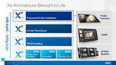
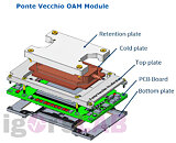
Intel's upcoming Ponte Vecchio graphics card is set to be the company's most powerful processor ever designed, and the chip is indeed looking like an engineering marvel. From Intel's previous teasers, we have learned that Ponte Vecchio is built using 47 "magical tiles" or 47 dies which are responsible either for computing elements, Rambo Cache, Xe links, or something else. Today, we are getting a new piece of information coming from Igor's LAB, regarding the Ponte Vecchio and some of its design choices. For starters, the GPU will be a heterogeneous design that consists out of many different nodes. Some parts of the GPU will be manufactured on Intel's 10 nm SuperFin and 7 nm technologies, while others will use TSMC's 7 nm and 5 nm nodes. The smaller and more efficient nodes will probably be used for computing elements. Everything will be held together by Intel's EMIB and Foveros 3D packaging.

Next up, we have information that this massive Intel processor will be accountable for around 600 Watts of heat output, which is a lot to cool. That is why in the leaked renders, we see that Intel envisioned these processors to be liquid-cooled, which would make the cooling much easier and much more efficient compared to air cooling of such a high heat output. Another interesting thing is that the Ponte Vecchio is designed to fit inside OAM (OCP Accelerator Module) form factor, an alternative to the regular PCIe-based accelerators in data centers. OAM is used primarily by hyper scalers like Facebook, Amazon, Google, etc., so we imagine that Intel already knows its customers before the product even hits the market.
Return to Keyword Browsing
May 1st, 2024 01:37 EDT change timezone

New Forum Posts

Popular Reviews

Controversial News Posts