News Posts matching #CDNA

Return to Keyword Browsing

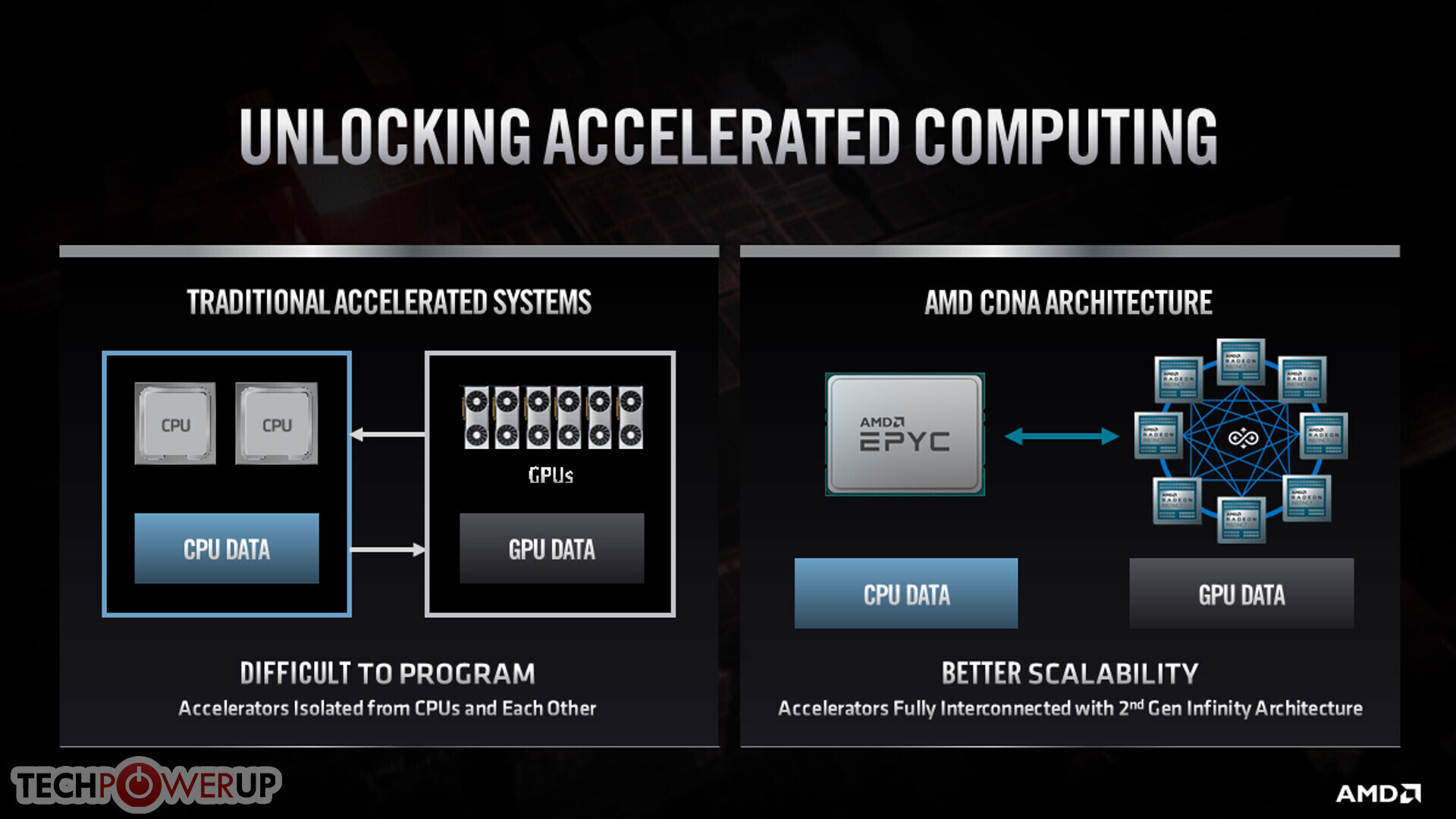
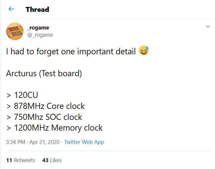
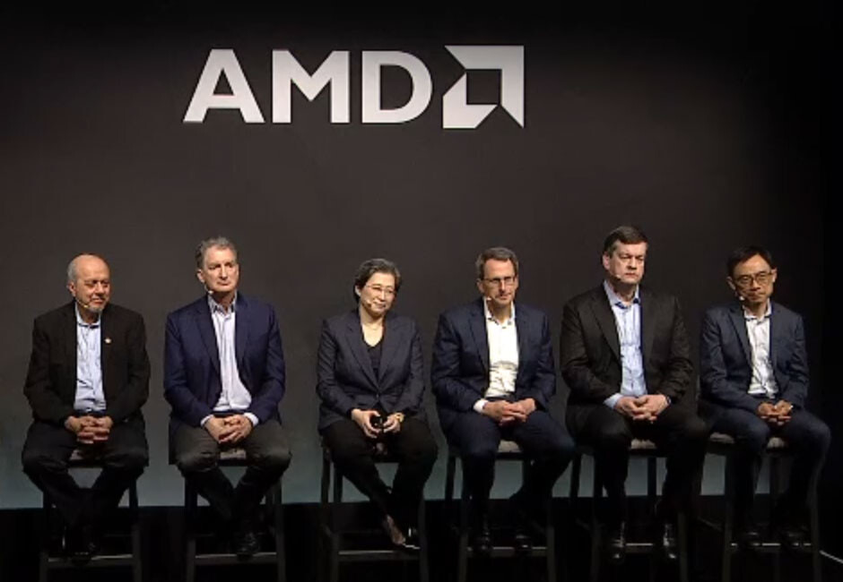
Dr. Lisa Su Responds to TinyBox's Radeon RX 7900 XTX GPU Firmware Problems

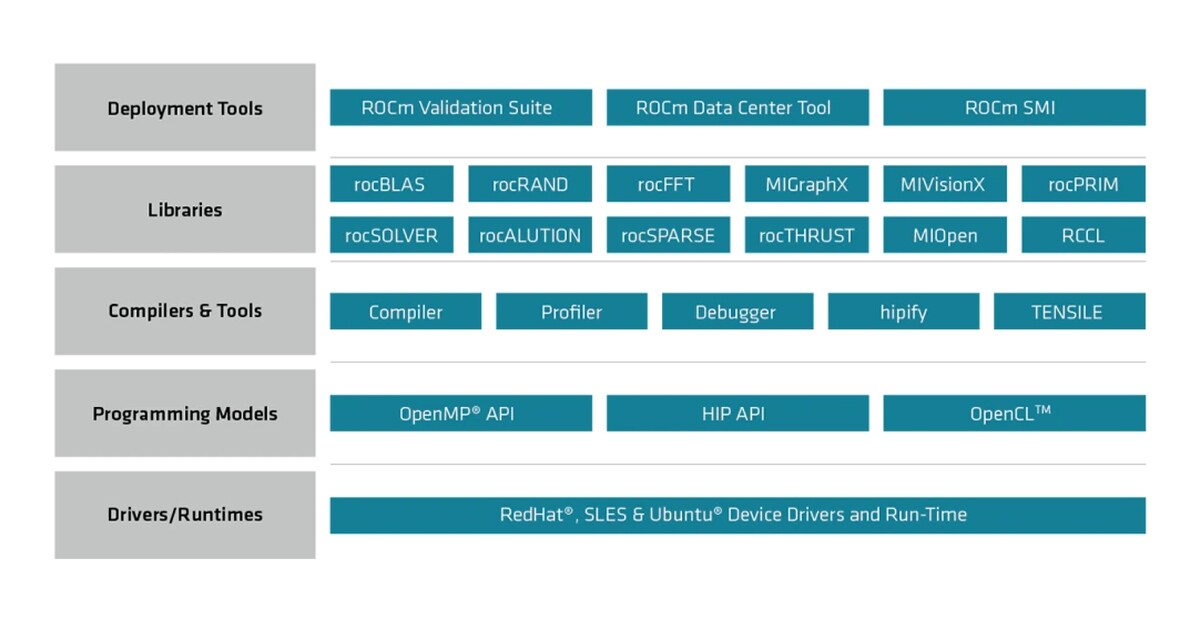
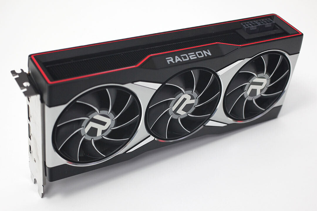
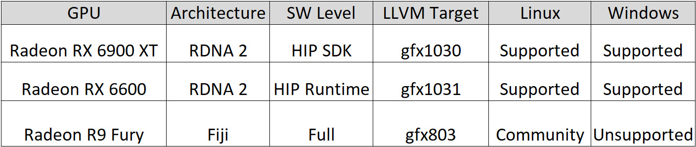
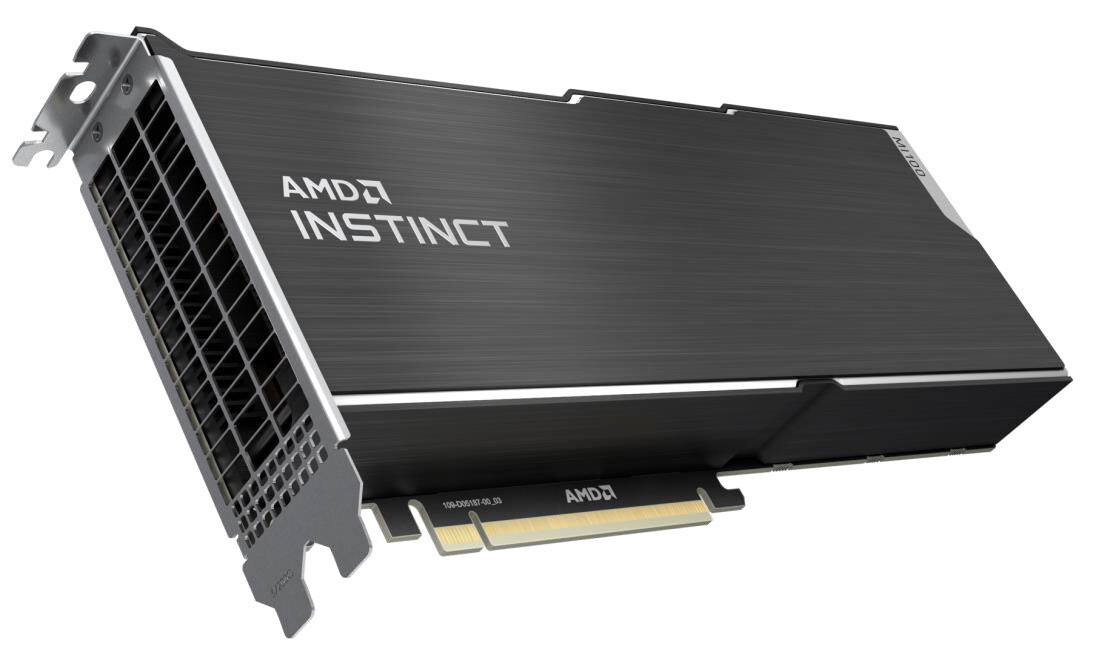
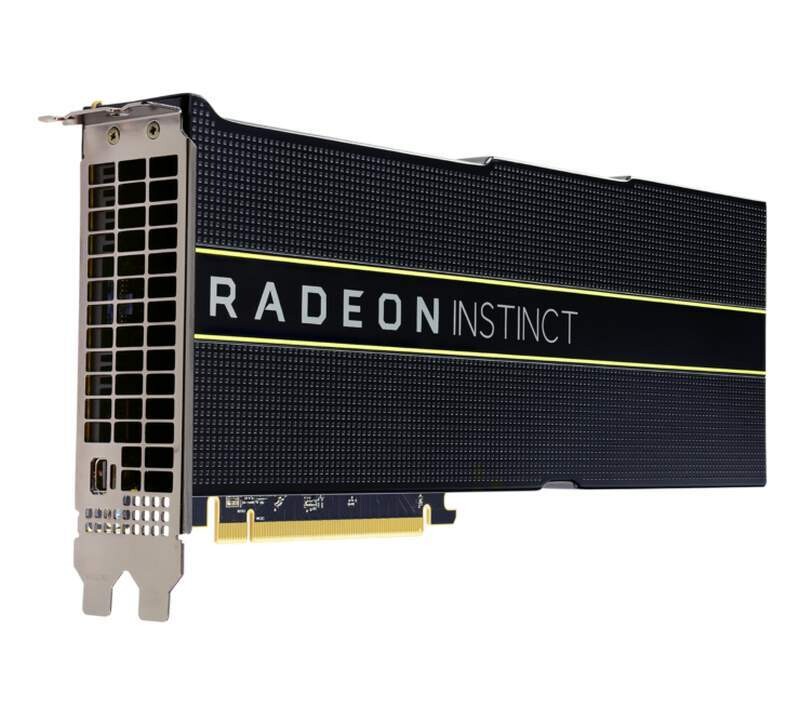
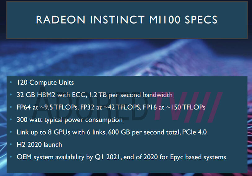
The TinyBox AI server system attracted plenty of media attention last week—its creator, George Hotz, decided to build with AMD RDNA 3.0 GPU hardware rather than the expected/traditional choice of CDNA 3.0. Tiny Corp. is a startup firm dealing in neural network frameworks—they currently "write and maintain tinygrad." Hotz & Co. are in the process of assembling rack-mounted 12U TinyBox systems for customers—an individual server houses an AMD EPYC 7532 processor and six XFX Speedster MERC310 Radeon RX 7900 XTX graphics cards. The Tiny Corp. social media account has engaged in numerous NVIDIA vs. AMD AI hardware debates/tirades—Hotz appears to favor the latter, as evidenced in his latest choice of components. ROCm support on Team Red AI Instinct accelerators is fairly mature at this point in time, but a much newer prospect on gaming-oriented graphics cards.

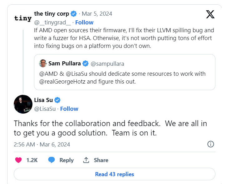
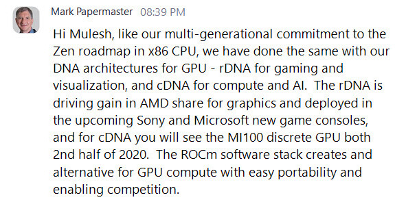
Tiny Corporation's unusual leveraging of Radeon RX 7900 XTX GPUs in a data center configuration has already hit a developmental roadblock. Yesterday, the company's social media account expressed driver-related frustrations in a public forum: "If AMD open sources their firmware, I'll fix their LLVM spilling bug and write a fuzzer for HSA. Otherwise, it's not worth putting tons of effort into fixing bugs on a platform you don't own." Hotz's latest complaint was taken onboard by AMD's top brass—Dr. Lisa Su responded with the following message: "Thanks for the collaboration and feedback. We are all in to get you a good solution. Team is on it." Her software engineers—within a few hours—managed to fling out a set of fixes in Tiny Corporation's direction. Hotz appreciated the quick turnaround, and proceeded to run a model without encountering major stability issues: "AMD sent me an updated set of firmware blobs to try. They are responsive, and there have been big strides in the driver in the last year. It will be good! This training run is almost 5 hours in, hasn't crashed yet." Tiny Corp. drummed up speculation about AMD open sourcing GPU MES firmware—Hotz disclosed that he will be talking (on the phone) to Team Red leadership.

AMD Delivers Leadership Portfolio of Data Center AI Solutions with AMD Instinct MI300 Series

Today, AMD announced the availability of the AMD Instinct MI300X accelerators - with industry leading memory bandwidth for generative AI and leadership performance for large language model (LLM) training and inferencing - as well as the AMD Instinct MI300A accelerated processing unit (APU) - combining the latest AMD CDNA 3 architecture and "Zen 4" CPUs to deliver breakthrough performance for HPC and AI workloads.

"AMD Instinct MI300 Series accelerators are designed with our most advanced technologies, delivering leadership performance, and will be in large scale cloud and enterprise deployments," said Victor Peng, president, AMD. "By leveraging our leadership hardware, software and open ecosystem approach, cloud providers, OEMs and ODMs are bringing to market technologies that empower enterprises to adopt and deploy AI-powered solutions."

GIGABYTE Unveils Next-gen HPC & AI Servers with AMD Instinct MI300 Series Accelerators

GIGABYTE Technology: Giga Computing, a subsidiary of GIGABYTE and an industry leader in high-performance servers, and IT infrastructure, today announced the GIGABYTE G383-R80 for the AMD Instinct MI300A APU and two GIGABYTE G593 series servers for the AMD Instinct MI300X GPU and AMD EPYC 9004 Series processor. As a testament to the performance of AMD Instinct MI300 Series family of products, the El Capitan supercomputer at Lawrence Livermore National Laboratory uses the MI300A APU to power exascale computing. And these new GIGABYTE servers are the ideal platform to propel discoveries in HPC & AI at exascale.⁠

Marrying of a CPU & GPU: G383-R80
For incredible advancements in HPC there is the GIGABYTE G383-R80 that houses four LGA6096 sockets for MI300A APUs. This chip integrates a CPU that has twenty-four AMD Zen 4 cores with a powerful GPU built with AMD CDNA 3 GPU cores. And the chiplet design shares 128 GB of unified HBM3 memory for impressive performance for large AI models. The G383 server has lots of expansion slots for networking, storage, or other accelerators, with a total of twelve PCIe Gen 5 slots. And in the front of the chassis are eight 2.5" Gen 5 NVMe bays to handle heavy workloads such as real-time big data analytics and latency-sensitive workloads in finance and telecom. ⁠

Two-ExaFLOP El Capitan Supercomputer Starts Installation Process with AMD Instinct MI300A

When Lawrence Livermore National Laboratory (LLNL) announced the creation of a two-ExaFLOP supercomputer named El Capitan, we heard that AMD would power it with its Instinct MI300 accelerator. Today, LNLL published a Tweet that states, "We've begun receiving & installing components for El Capitan, @NNSANews' first #exascale #supercomputer. While we're still a ways from deploying it for national security purposes in 2024, it's exciting to see years of work becoming reality." As published images show, HPE racks filled with AMD Instinct MI300 are showing up now at LNLL's facility, and the supercomputer is expected to go operational in 2024. This could mean that November 2023 TOP500 list update wouldn't feature El Capitan, as system enablement would be very hard to achieve in four months until then.

The El Capitan supercomputer is expected to run on AMD Instinct MI300A accelerator, which features 24 Zen4 cores, CDNA3 architecture, and 128 GB of HBM3 memory. All paired together in a four-accelerator configuration goes inside each node from HPE, also getting water cooling treatment. While we don't have many further details on the memory and storage of El Capitan, we know that the system will exceed two ExFLOPS at peak and will consume close to 40 MW of power.

AMD Confirms that Instinct MI300X GPU Can Consume 750 W

AMD recently revealed its Instinct MI300X GPU at their Data Center and AI Technology Premiere event on Tuesday (June 15). The keynote presentation did not provide any details about the new accelerator model's power consumption, but that did not stop one tipster - Hoang Anh Phu - from obtaining this information from Team Red's post-event footnotes. A comparative observation was made: "MI300X (192 GB HBM3, OAM Module) TBP is 750 W, compared to last gen, MI250X TBP is only 500-560 W." A leaked Giga Computing roadmap from last month anticipated server-grade GPUs hitting the 700 W mark.

NVIDIA's Hopper H100 took the crown - with its demand for a maximum of 700 W - as the most power-hungry data center enterprise GPU until now. The MI300X's OCP Accelerator Module-based design now surpasses Team Green's flagship with a slightly greater rating. AMD's new "leadership generative AI accelerator" sports 304 CDNA 3 compute units, which is a clear upgrade over the MI250X's 220 (CDNA 2) CUs. Engineers have also introduced new 24G B HBM3 stacks, so the MI300X can be specced with 192 GB of memory (as a maximum), the MI250X is limited to a 128 GB memory capacity with its slower HBM2E stacks. We hope to see sample units producing benchmark results very soon, with the MI300X pitted against H100.

AMD ROCm 5.5 Now Available on GitHub

As expected with AMD's activity on GitHub, ROCm 5.5 has now been officially released. It brings several big changes, including better RDNA 3 support. While officially focused on AMD's professional/workstation graphics cards, the ROCm 5.5 should also bring better support for Radeon RX 7000 series graphics cards on Linux.

Surprisingly, the release notes do not officially mention RDNA 3 improvements in its release notes, but those have been already tested and confirmed. The GPU support list is pretty short including AMD GFX9, RDNA, and CDNA GPUs, ranging from Radeon VII, Pro VII, W6800, V620, and Instinct lineup. The release notes do mention new HIP enhancements, enhanced stack size limit, raising it from 16k to 128k, new APIs, OpenMP enhancements, and more. You can check out the full release notes, downloads, and more details over at GitHub.

AMD Brings ROCm to Consumer GPUs on Windows OS

AMD has published an exciting development for its Radeon Open Compute Ecosystem (ROCm) users today. Now, ROCm is coming to the Windows operating system, and the company has extended ROCm support for consumer graphics cards instead of only supporting professional-grade GPUs. This development milestone is essential for making AMD's GPU family more competent with NVIDIA and its CUDA-accelerated GPUs. For those unaware, AMD ROCm is a software stack designed for GPU programming. Similarly to NVIDIA's CUDA, ROCm is designed for AMD GPUs and was historically limited to Linux-based OSes and GFX9, CDNA, and professional-grade RDNA GPUs.

However, according to documents obtained by Tom's Hardware (which are behind a login wall), AMD has brought support for ROCm to Radeon RX 6900 XT, Radeon RX 6600, and R9 Fury GPU. What is interesting is not the inclusion of RX 6900 XT and RX 6600 but the support for R9 Fury, an eight-year-old graphics card. Also, what is interesting is that out of these three GPUs, only R9 Fury has full ROCm support, the RX 6900 XT has HIP SDK support, and RX 6600 has only HIP runtime support. And to make matters even more complicated, the consumer-grade R9 Fury GPU has full ROCm support only on Linux and not Windows. The reason for this strange selection of support has yet to be discovered. However, it is a step in the right direction, as AMD has yet to enable more functionality on Windows and more consumer GPUs to compete with NVIDIA.

AMD Shows Instinct MI300 Exascale APU with 146 Billion Transistors

During its CES 2023 keynote, AMD announced its latest Instinct MI300 APU, a first of its kind in the data center world. Combining the CPU, GPU, and memory elements into a single package eliminates latency imposed by long travel distances of data from CPU to memory and from CPU to GPU throughout the PCIe connector. In addition to solving some latency issues, less power is needed to move the data and provide greater efficiency. The Instinct MI300 features 24 Zen4 cores with simultaneous multi-threading enabled, CDNA3 GPU IP, and 128 GB of HBM3 memory on a single package. The memory bus is 8192-bit wide, providing unified memory access for CPU and GPU cores. CLX 3.0 is also supported, making cache-coherent interconnecting a reality.

The Instinct MI300 APU package is an engineering marvel of its own, with advanced chiplet techniques used. AMD managed to do 3D stacking and has nine 5 nm logic chiplets that are 3D stacked on top of four 6 nm chiplets with HBM surrounding it. All of this makes the transistor count go up to 146 billion, representing the sheer complexity of a such design. For performance figures, AMD provided a comparison to Instinct MI250X GPU. In raw AI performance, the MI300 features an 8x improvement over MI250X, while the performance-per-watt is "reduced" to a 5x increase. While we do not know what benchmark applications were used, there is a probability that some standard benchmarks like MLPerf were used. For availability, AMD targets the end of 2023, when the "El Capitan" exascale supercomputer will arrive using these Instinct MI300 APU accelerators. Pricing is unknown and will be unveiled to enterprise customers first around launch.

AMD Instinct MI300 APU to Power El Capitan Exascale Supercomputer

The Exascale supercomputing race is now well underway, as the US-based Frontier supercomputer got delivered, and now we wait to see the remaining systems join the race. Today, during 79th HPC User Forum at Oak Ridge National Laboratory (ORNL), Terri Quinn at Lawrence Livermore National Laboratory (LLNL) delivered a few insights into what El Capitan exascale machine will look like. And it seems like the new powerhouse will be based on AMD's Instinct MI300 APU. LLNL targets peak performance of over two exaFLOPs and a sustained performance of more than one exaFLOP, under 40 megawatts of power. This should require a very dense and efficient computing solution, just like the MI300 APU is.

As a reminder, the AMD Instinct MI300 is an APU that combines Zen 4 x86-64 CPU cores, CDNA3 compute-oriented graphics, large cache structures, and HBM memory used as DRAM on a single package. This is achieved using a multi-chip module design with 2.5D and 3D chiplet integration using Infinity architecture. The system will essentially utilize thousands of these APUs to become one large Linux cluster. It is slated for installation in 2023, with an operating lifespan from 2024 to 2030.

Alleged AMD Instinct MI300 Exascale APU Features Zen4 CPU and CDNA3 GPU

Today we got information that AMD's upcoming Instinct MI300 will be allegedly available as an Accelerated Processing Unit (APU). AMD APUs are processors that combine CPU and GPU into a single package. AdoredTV managed to get ahold of a slide that indicates that AMD Instinct MI300 accelerator will also come as an APU option that combines Zen4 CPU cores and CDNA3 GPU accelerator in a single, large package. With technologies like 3D stacking, MCM design, and HBM memory, these Instinct APUs are positioned to be a high-density compute the product. At least six HBM dies are going to be placed in a package, with the APU itself being a socketed design.

The leaked slide from AdoredTV indicates that the first tapeout is complete by the end of the month (presumably this month), with the first silicon hitting AMD's labs in Q3 of 2022. If the silicon turns out functional, we could see these APUs available sometime in the first half of 2023. Below, you can see an illustration of the AMD Instinct MI300 GPU. The APU version will potentially be of the same size with Zen4 and CDNA3 cores spread around the package. As Instinct MI300 accelerator is supposed to use eight compute tiles, we could see different combinations of CPU/GPU tiles offered. As we await the launch of the next-generation accelerators, we are yet to see what SKUs AMD will bring.

AMD Introduces Instinct MI210 Data Center Accelerator for Exascale-class HPC and AI in a PCIe Form-Factor

AMD today announced a new addition to the Instinct MI200 family of accelerators. Officially titled Instinct MI210 accelerator, AMD tries to bring exascale-class technologies to mainstream HPC and AI customers with this model. Based on CDNA2 compute architecture built for heavy HPC and AI workloads, the card features 104 compute units (CUs), totaling 6656 Streaming Processors (SPs). With a peak engine clock of 1700 MHz, the card can output 181 TeraFLOPs of FP16 half-precision peak compute, 22.6 TeraFLOPs peak FP32 single-precision, and 22.6 TFLOPs peak FP62 double-precision compute. For single-precision matrix (FP32) compute, the card can deliver a peak of 45.3 TFLOPs. The INT4/INT8 precision settings provide 181 TOPs, while MI210 can compute the bfloat16 precision format with 181 TeraFLOPs at peak.

The card uses a 4096-bit memory interface connecting 64 GBs of HMB2e to the compute silicon. The total memory bandwidth is 1638.4 GB/s, while memory modules run at a 1.6 GHz frequency. It is important to note that the ECC is supported on the entire chip. AMD provides an Instinct MI210 accelerator as a PCIe solution, based on a PCIe 4.0 standard. The card is rated for a TDP of 300 Watts and is cooled passively. There are three infinity fabric links enabled, and the maximum bandwidth of the infinity fabric link is 100 GB/s. Pricing is unknown; however, availability is March 22nd, which is the immediate launch date.

AMD places this card directly aiming at NVIDIA A100 80 GB accelerator as far as the targeted segment, with emphasis on half-precision and INT4/INT8 heavy applications.

NVIDIA to Split Graphics and Compute Architecture Naming, "Blackwell" Architecture Spotted

The recent NVIDIA data-leak springs up information on various upcoming graphics parts. Besides "Ada Lovelace," "Hopper," we come across a new codename, "Blackwell." It turns out that NVIDIA is splitting the the graphics and compute architecture naming with the next generation, not unlike what AMD did, with its RDNA and CDNA series. The current "Ampere" architecture is being used both for compute and graphics, with the streaming multiprocessor for the two being slightly different—the compute "Ampere" has more FP64 and Tensor components, while the graphics "Ampere" does away with these in favor of RT cores and graphics-relevant components.

The graphics architecture to succeed GeForce "Ampere" will be GeForce "Ada Lovelace." GPUs in this series are identified in the leaked code as "AD102," "AD103," "AD104," "AD106," "AD107," and "AD10B," succeeding a similar numbering for parts with the "A" (GeForce Ampere) series. The compute architecture succeeding "Ampere" will be codenamed "Hopper." with parts in the series being codenamed "GH100" and "GH202." Another compute or datacenter architecture is "Blackwell," with parts being codenamed "GB100" and "GB102." From all accounts, NVIDIA is planning to launch the GeForce 40-series "Ada" graphics card lineup in the second half of 2022. The company is in need of a similar refresh for its compute product lineup, and could debut "Hopper" either toward the end of 2022 or next year. "Blackwell" could follow "Hopper."

AMD to Implement TSMC SoIC Tech With Upcoming HPC Chips

AMD will debut TSMC's ambitious System-on-Integrated-Chips (SoIC) technology with its upcoming HPC chips, according to a DigiTimes report. A step toward rivaling Intel's Foveros 3-D chip stacking technology, SoIC will enable AMD to stack logic, memory, and I/O as separate chips within a single package. The article references a next-generation "HPC" chip, although it didn't delve into what this could be. Logically, AMD would want to integrate its EPYC and MI accelerator lines into a single package that can be used in HPCs. Such a product would combine its Zen-series x86-64 serial processing, with CDNA-series scalar processing, expertise in memory, leveraging large on-die victim-caches, and high-bandwidth memory (HBM); along with next-gen I/O.

AMD Instinct MI200 to Launch This Year with MCM Design

AMD is slowly preparing the next-generation of its compute-oriented flagship graphics card design called Instinct MI200 GPU. It is the card of choice for the exascale Frontier supercomputer, which is expected to make a debut later this year at the Oak Ridge Leadership Computing Facility. With the supercomputer planned for the end of this year, AMD Instinct MI200 is also going to get launched eight a bit before or alongside it. The Frontier exascale supercomputer is supposed to bring together AMD's next-generation Trento EPYC CPUs with Instinct MI200 GPU compute accelerators. However, it seems like AMD will utilize some new technologies for the making of this supercomputer. While we do not know what Trento EPYC CPUs will look like, it seems like Instinct MI200 GPU is going to feature a multi-chip-module (MCM) design with the new CDNA 2 GPU architecture. With this being the only information about the GPU, we have to wait a bit to find out more details.
AMD CDNA Die

AMD Announces CDNA Architecture. Radeon MI100 is the World's Fastest HPC Accelerator

AMD today announced the new AMD Instinct MI100 accelerator - the world's fastest HPC GPU and the first x86 server GPU to surpass the 10 teraflops (FP64) performance barrier. Supported by new accelerated compute platforms from Dell, Gigabyte, HPE, and Supermicro, the MI100, combined with AMD EPYC CPUs and the ROCm 4.0 open software platform, is designed to propel new discoveries ahead of the exascale era.

Built on the new AMD CDNA architecture, the AMD Instinct MI100 GPU enables a new class of accelerated systems for HPC and AI when paired with 2nd Gen AMD EPYC processors. The MI100 offers up to 11.5 TFLOPS of peak FP64 performance for HPC and up to 46.1 TFLOPS peak FP32 Matrix performance for AI and machine learning workloads. With new AMD Matrix Core technology, the MI100 also delivers a nearly 7x boost in FP16 theoretical peak floating point performance for AI training workloads compared to AMD's prior generation accelerators.

AMD Eyes Mid-November CDNA Debut with Instinct MI100, "World's Fastest FP64 Accelerator"

AMD is eyeing a mid-November debut for its CDNA compute architecture with the Instinct MI100 compute accelerator card. CDNA is a fork of RDNA for headless GPU compute accelerators with large SIMD resources. An Aroged report pins the launch of the MI100 at November 16, 2020, according to leaked AMD documents it dug up. The Instinct MI100 will eye a slice of the same machine intelligence pie NVIDIA is seeking to dominate with its A100 Tensor Core compute accelerator.

It appears like the first MI100 cards will be built in the add-in-board form-factor with PCI-Express 4.0 x16 interfaces, although older reports do predict AMD creating a socketed variant of its Infinity Fabric interconnect for machines with larger numbers of these compute processors. In the leaked document, AMD claims that the Instinct MI100 is the "world's highest double-precision accelerator for machine learning, HPC, cloud compute, and rendering systems." This is an especially big claim given that the A100 Tensor Core features FP64 CUDA cores based on the "Ampere" architecture. Then again, given that AMD claims that the RDNA2 graphics architecture is clawing back at NVIDIA with performance at the high-end, the competitiveness of the Instinct MI100 against the A100 Tensor Core cannot be discounted.

AMD Radeon MI100 "Arcturus" Alleged Specification Listed, the GPU Could be Coming in December

AMD has been preparing to launch its MI100 accelerator and fight NVIDIA's A100 Ampere GPU in machine learning and AI horizon, and generally compute-intensive workloads. According to some news sources over at AdoredTV, the GPU alleged specifications were listed, along with some slides about the GPU which should be presented at the launch. So to start, this is what we have on the new Radeon MI100 "Arcturus" GPU based on CDNA architecture. The alleged specifications mention that the GPU will feature 120 Compute Units (CUs), meaning that if the GPU keeps the 64-core per CU configuration, we are looking at 7680 cores powered by CDNA architecture.

The leaked slide mentions that the GPU can put out as much as 42 TeraFLOPs of FP32, single-precision compute. This makes it more than twice as fast compared to NVIDIA's A100 GPU at FP32 workloads. To achieve that, the card would need to have all of its 7680 cores running at 2.75 GHz, which would be a bit high number. On the same slide, the GPU is claimed to have 9.5 TeraFLOPs of FP64 dual-precision performance, while the FP16 power is going to be around 150 TeraFLOPs. For comparison, the A100 GPU from NVIDIA features 9.7 TeraFLOPS of FP64, 19.5 TeraFLOPS of FP32, and 312 (or 634 with sparsity enabled) TeraFLOPs of FP16 compute. AMD GPU is allegedly only more powerful for FP32 workloads, where it outperforms the NVIDIA card by 2.4 times. And if that is really the case, AMD has found its niche in the HPC sector, and it plans to dominate there. According to AdoredTV sources, the GPU could be coming in December of this year.

AMD Confirms "Zen 4" on 5nm, Other Interesting Tidbits from Q2-2020 Earnings Call

AMD late Tuesday released its Q2-2020 financial results, which saw the company rake in revenue of $1.93 billion for the quarter, and clock a 26 percent YoY revenue growth. In both its corporate presentation targeted at the financial analysts, and its post-results conference call, AMD revealed a handful interesting bits looking into the near future. Much of the focus of AMD's presentation was in reassuring investors that [unlike Intel] it is promising a stable and predictable roadmap, that nothing has changed on its roadmap, and that it intends to execute everything on time. "Over the past couple of quarters what we've seen is that they see our performance/capability. You can count on us for a consistent roadmap. Milan point important for us, will ensure it ships later this year. Already started engaging people on Zen4/5nm. We feel customers are very open. We feel well positioned," said president and CEO Dr Lisa Su.

For starters, there was yet another confirmation from the CEO that the company will launch the "Zen 3" CPU microarchitecture across both the consumer and data-center segments before year-end, which means both Ryzen and EPYC "Milan" products based on "Zen 3." Also confirmed was the introduction of the RDNA2 graphics architecture across consumer graphics segments, and the debut of the CDNA scalar compute architecture. The company started shipping semi-custom SoCs to both Microsoft and Sony, so they could manufacture their next-generation Xbox Series X and PlayStation 5 game consoles in volumes for the Holiday shopping season. Semi-custom shipments could contribute big to the company's Q3-2020 earnings. CDNA won't play a big role in 2020 for AMD, but there will be more opportunities for the datacenter GPU lineup in 2021, according to the company. CDNA2 debuts next year.

AMD Confirms CDNA-Based Radeon Instinct MI100 Coming to HPC Workloads in 2H2020

Mark Papermaster, chief technology officer and executive vice president of Technology and Engineering at AMD, today confirmed that CDNA is on-track for release in 2H2020 for HPC computing. The confirmation was (adequately) given during Dell's EMC High-Performance Computing Online event. This confirms that AMD is looking at a busy 2nd half of the year, with both Zen 3, RDNA 2 and CDNA product lines being pushed to market.

CDNA is AMD's next push into the highly-lucrative HPC market, and will see the company differentiating their GPU architectures through market-based product differentiation. CDNA will see raster graphics hardware, display and multimedia engines, and other associated components being removed from the chip design in a bid to recoup die area for both increased processing units as well as fixed-function tensor compute hardware. CNDA-based Radeon Instinct MI100 will be fabricated under TSMC's 7 nm node, and will be the first AMD architecture featuring shared memory pools between CPUs and GPUs via the 2nd gen Infinity Fabric, which should bring about both throughput and power consumption improvements to the platform.

Distant Blips on the AMD Roadmap Surface: Rembrandt and Raphael

Several future AMD processor codenames across various computing segments surfaced courtesy of an Expreview leak that's largely aligned with information from Komachi Ensaka. It does not account for "Matisse Refresh" that's allegedly coming out in June-July as three gaming-focused Ryzen socket AM4 desktop processors; but roadmap from 2H-2020 going up to 2022 sees many codenames surface. To begin with, the second half of 2020 promises to be as action packed as last year's 7/7 mega launch. Over in the graphics business, the company is expected to debut its DirectX 12 Ultimate-compliant RDNA2 client graphics, and its first CDNA architecture-based compute accelerators. Much of the processor launch cycle is based around the new "Zen 3" microarchitecture.

The server platform debuting in the second half of 2020 is codenamed "Genesis SP3." This will be the final processor architecture for the SP3-class enterprise sockets, as it has DDR4 and PCI-Express gen 4.0 I/O. The EPYC server processor is codenamed "Milan," and combines "Zen 3" chiplets along with an sIOD. EPYC Embedded (FP6 package) processors are codenamed "Grey Hawk."

AMD's Next-Generation Radeon Instinct "Arcturus" Test Board Features 120 CUs

AMD is preparing to launch its next-generation of Radeon Instinct GPUs based on the new CDNA architecture designed for enterprise deployments. Thanks to the popular hardware leaker _rogame (@_rogame) we have some information about the configuration of the upcoming Radeon Instinct MI100 "Arcturus" server GPU. Previously, we obtained the BIOS of the Arcturus GPU that showed a configuration of 128 Compute Units (CUs), which resulted in 8,192 of CDNA cores. That configuration had a specific setup of 1334 MHz GPU clock, SoC frequency of 1091 MHz, and memory speed of 1000 MHz. However, there was another GPU test board spotted which featured a bit different specification.

The reported configuration is an Arcturus GPU with 120 CUs, resulting in a CDNA core count of 7,680 cores. These cores are running at frequencies of 878 MHz for the core clock, 750 MHz SoC clock, and a surprising 1200 MHz memory clock. While the SoC and core clocks are lower than the previous report, along with the CU count, the memory clock is up by 200 MHz. It is important to note that this is just a test board/variation of the MI100, and actual frequencies should be different.
AMD Radeon Instinct MI60

AMD Announces the CDNA and CDNA2 Compute GPU Architectures

AMD at its 2020 Financial Analyst Day event unveiled its upcoming CDNA GPU-based compute accelerator architecture. CDNA will complement the company's graphics-oriented RDNA architecture. While RDNA powers the company's Radeon Pro and Radeon RX client- and enterprise graphics products, CDNA will power compute accelerators such as Radeon Instinct, etc. AMD is having to fork its graphics IP to RDNA and CDNA due to what it described as market-based product differentiation.

Data centers and HPCs using Radeon Instinct accelerators have no use for the GPU's actual graphics rendering capabilities. And so, at a silicon level, AMD is removing the raster graphics hardware, the display and multimedia engines, and other associated components that otherwise take up significant amounts of die area. In their place, AMD is adding fixed-function tensor compute hardware, similar to the tensor cores on certain NVIDIA GPUs.
AMD Datacenter GPU Roadmap CDNA CDNA2 AMD CDNA Architecture AMD Exascale Supercomputer

AMD Financial Analyst Day 2020 Live Blog

AMD Financial Analyst Day presents an opportunity for AMD to talk straight with the finance industry about the company's current financial health, and a taste of what's to come. Guidance and product teasers made during this time are usually very accurate due to the nature of the audience. In this live blog, we will post information from the Financial Analyst Day 2020 as it unfolds.
20:59 UTC: The event has started as of 1 PM PST. CEO Dr Lisa Su takes stage.
Return to Keyword Browsing
May 1st, 2024 06:46 EDT change timezone

New Forum Posts

Popular Reviews

Controversial News Posts