News Posts matching #IBM
Return to Keyword Browsing

IBM is launching a free multiplayer online game (
PowerUp) challenging teenagers to help save the planet "Helios" from ecological disaster. The game is part of IBM's TryScience initiative and will be launched at Engineer's Week 2008 opening on February 16 in Washington, D.C. The game, which can be played alone or together, features a planet in near ecological ruin where three exciting missions for solar, wind and water power must be solved before sandstorms, floods or SmogGobs thwart the rescue.
IBM was never known for making anything small. From some of the very first computers to the PlayStation 3 processor, IBM is one of the largest influences of the tech industry. As if to add to this success, IBM wants to be a host: to the entire internet. The thought is, at first, silly, and then unfathomable. How can one computer, let alone one company, run the entire internet? IBM claims they can pull it off with a heavily modified Blue Gene computer, which they have codenamed "Kittyhawk". The processing power of Kittyhawk would be immense. The software is too complex to explain, and will be left at "Kittyhawk will run the internet as a single application". As far as hardware is concerned, current estimates say that Kittyhawk will need 67.1 million cores and 32PB of memory.
IBM Cell BE PS3 Processor Shrunk to 45nm
At an ISSCC session yesterday afternoon, IBM announced details of a smaller, lower-power version of the Cell BE processor that powers Sony's PlayStation 3 entertainment system. The Cell BE is currently fabricated on IBM's 65nm SOI process, but IBM will soon move the console chip onto the company's next-generation 45nm high-k process. The 45nm Cell will use about 40 percent less power than its 65nm predecessor, and its die area will be reduced by 34 percent. The greatly reduced power budget will cut down on the amount of active cooling required by the console, which in turn will make it cheaper to produce and more reliable. Also affecting Sony's per-unit cost is the reduction in overall die size. A smaller die means a smaller, cheaper package; it also means that yields will be better and that each chip will cost less overall. All this will help Sony to slash the production cost of every PLAYSTATION3 console. Will this affect end users, only time will show. New price cuts or new PS3 models, haven't been officially announced yet.
Industry analysts, and sources, have speculated about the possible creation of a more formal relationship between IBM and AMD. Such a relationship may result in a possible merger between the two companies in the future. An IBM takeover, or joint venture company may result. Such a merger would allow IBM to maintain ties to some management in the computer industry as the company moves more toward technology services. The creation of some sort of more formal association could help inject confidence into AMD which has not reported a quarterly profit since mid-2006. IBM and AMD have been technology partners for several years, and are currently completing a joint manufacturing plant in Malta.
IBM today announced that it will offer an integrated Open Collaboration Client Solution with support for Ubuntu, a Linux-based operating system from Canonical Ltd. that is especially popular for desktops, laptops and thin clients. Showing strong momentum around its IBM Lotus Notes 8 and IBM Lotus Symphony-based Open Collaboration Client Solution, IBM also announced a new agreement working with Red Hat targeting small and medium-sized enterprises, and momentum in the Open Collaboration Client Solution powered by SUSE Linux Enterprise from Novell that was announced in August 2007. The announcements were made at the opening of Lotusphere in Orlando.
IBM today announced it has acquired XIV, a privately held storage technology company based in Tel Aviv, Israel. XIV, its technologies and employees, will become part of the IBM System Storage business unit of the IBM Systems and Technology Group. Financial terms of the acquisition are not being disclosed. "The acquisition of XIV will further strengthen the IBM infrastructure portfolio long term and put IBM in the best position to address emerging storage opportunities like Web 2.0 applications, digital archives and digital media," said Andy Monshaw, general manager, IBM System Storage.
IBM has licensed its next-generation technology for manufacturing processors to Semiconductor Manufacturing International Corp., the largest Chinese chipmaker, the companies said Wednesday. The partnership spotlights the growing technical abilities in China, a country that's already a manufacturing powerhouse for lower-tech products. Terms of the IBM deal weren't disclosed. "We are excited about the SMIC-IBM licensing partnership, which will accelerate SMIC technology advancement in logic process technology and help us provide optimal solutions for our customers at our 300mm facilities," said Matthew Szymanski, vice president of corporate relations for Shanghai-based SMIC, in a statement. "China is a rapidly growing, strategic marketplace, and SMIC is the largest Chinese foundry," said Kevin Hutchings, IBM's vice president of intellectual property licensing.

Toshiba has joined a group led by International Business Machines Corp. (IBM) to jointly develop 32nm chips, following the trend of manufacturers banding together to keep escalating research costs down. The alliance also comprises Advanced Micro Devices, Samsung Electronics, Singapore's Chartered Semiconductor Manufacturing, Germany's Infineon Technologies AG and privately owned U.S.-based Freescale Semiconductor Inc. The seven companies have agreed to work through 2010 to design, develop and produce chips using tiny circuitry. Using smaller circuit sizes helps boost chip makers' productivity by making smaller chips more powerful, but the move to smaller sizes is becoming too difficult and expensive for a single manufacturer to undergo alone.

IBM made a major announcement today that they will be offering 32nm chips to their partners in the second half of 2009. This would mean that possibly the Xbox 360 could get even smaller chips than the 65nm "Falcon" CPUs. These new chips will up the power savings to 45% and speed boosts up to 30% over IBM's last generation of hardware. This will reduce the overheating issues, and maybe even make way for a smaller console. Consider this as rumour since there's no any official information from Microsoft, or any of the Xbox 360 OEMs.
IBM has revealed that it is working on a new 32nm processor manufacturing technique which could make the production of chips more accessible to smaller companies, as well as yielding performance gains. The process works in a similar way to the high-k/metal gate technique that is currently used by both IBM and Intel for their 45nm chips, which replaces some of the silicon in transistors with more efficient materials to pack more components into a single chip. IBM's new technique uses a modified version of this process known as high-k/gate-first to develop its 32nm chips, which works by focusing on the most advanced components first. Big Blue has already demonstrated a working example of the 32nm technology with prototype static RAM chips, and mass production is expected to begin during the second half of 2009.
IBM over the weekend announced it is quickly approaching $1 billion USD in revenue from the Indian market for the entire year of 2007. "We expect our revenues to reach USD one billion by the end of this calendar year up from 700 million in 2006 driven by strong factors. In the first three quarters of the current financial, the company's revenue has grown by over 39 per cent," said Jesse Green, IBM VP of Financial Management. During 2006, IBM had a growth rate of 37 percent in India, and grossed almost $700 million USD. The increase in revenue was helped by several major deals IBM made with companies in the nation throughout the year. IBM has deals with major telecom, realty and financial companies in India, with other announcements expected in 2008. "India is very important to us, not only for its domestic sales but providing a competitive cost structure and skills set to compete globally in the services businesses," Greene added. Furthermore, IBM expects to see India as the "hub for global delivery," allowing the company to conduct major research and development in the growing tech nation. The nation's evolution into a "hub" allows India to bring in added resources and technologies that used to go to other BRIC (Brazil, Russia, India, China)-type nations. IBM currently has 53,000 employees and 35 offices in India, making up one-seventh of the company's global workforce. The company had only 3,000 workers in 2002.
When a big company like ASUS has a patent infringement filed against it, it can often use its financial strength to overcome any problems. However, when the company filing the complaint is computer giant IBM, things start to look a bit worse. Earlier today, IBM filed a complaint against ASUS claiming that both its own-brand computers, as well as the contract computers its makes for other brands such as Apple and Dell, infringe upon three patents held by IBM. Big Blue was a little vague on the specifics of the patents, however it is asking the US government to ban imports of certain computers made by ASUS due to infringements regarding "important aspects of computer systems, including power supplies, computer cooling and computer clustering capabilities" on products including notebooks, servers, routers and some components. Apparently ASUS continued to sell computers using IBM's technology after a licensing agreement expired on 31st December 2004. ASUS has not yet commented on this matter.
Supercomputers that consist of thousands of individual processor "brains" connected by miles of copper wires could one day fit into a laptop PC, thanks in part to a breakthrough by IBM scientists announced today.
And while today's supercomputers can use the equivalent energy required to power hundreds of homes, these future tiny supercomputers-on-a-chip would expend the energy of a light bulb.
While companies probably get plenty of advertising revenue from putting previews in behind DVD movies, IBM seeks to go above and beyond the call of duty. IBM recently applied for a patent. If granted, IBM would own the means to essentially place commercials
in the middle of a DVD movie. You can read the exact workings of this new system by reading the
patent. IBM argues that such invasive and interruptive methods of advertising "may be a great source of advertising revenues that are not being tapped...revenues from DVD advertising may contribute to the reduction in cost of the DVDs." Of course, if IBM does start flooding DVDs with unwanted advertisements, chances are users will make their DVDs extremely cheap...by pirating them, thus avoiding the advertisements in the first place.
The world's most powerful line of supercomputers - IBM's Blue Gene family - is by far the most energy-efficient, according to a new ranking of the TOP500 computers. The inaugural
Green500 list ranks by energy efficiency the machines that make the overall TOP500 list of the world's fastest computers. The new Green500 list shows IBM Blue Gene supercomputers capturing 26 of the top 27 spots.
IBM and Cognos today announced that the two companies have entered into a definitive agreement for IBM to acquire Cognos, a publicly-held company based in Ottawa, Ontario, Canada, in an all-cash transaction at a price of approximately $5 billion USD or $58 USD per share, with a net transaction value of $4.9 billion USD. The acquisition is subject to Cognos shareholder approval, regulatory approvals and other customary closing conditions. It is expected to close in the first quarter of 2008.

After purchasing IBM's PC division three years ago Lenovo has continued to use the IBM brand until now. Although the agreement gave Lenovo rights to the IBM name until 2010 the company has now announced that, starting from next year it would drop the brand.
By making substantial progress on all of our critical priorities over the past few quarters, we're now a stronger, healthier company,
One important sign of this progress is our decision to completely transition our Think products from the IBM brand to the Lenovo brand two years earlier than planned.
said William Amelio, chief executive of Lenovo, in a press announcement relating to its quarterly results.
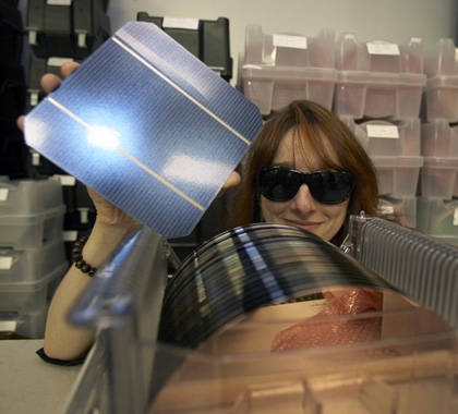
IBM today announced an innovative new semiconductor wafer reclamation process pioneered at its Burlington, Vermont manufacturing facility. The new process uses a specialized pattern removal technique to repurpose scrap semiconductor wafers -- thin discs of silicon material used to imprint patterns that make finished semiconductor chips for computers, mobile phones, video games, and other consumer electronics -- to a form used to manufacture silicon-based solar panels. The new process was recently awarded the "2007 Most Valuable Pollution Prevention Award" from The National Pollution Prevention Roundtable (NPPR).
IBM today announced a definitive agreement to acquire NovusCG, a privately held storage solutions company based in Manassas, Virginia. Financial terms were not disclosed. Novus will become part of the Storage and Data Services business unit in IBM Global Technology Services.
I.B.M. plans to mount its most ambitious challenge in years to Microsoft's dominance of personal computer software, by offering free programs for word processing, spreadsheets and presentations.
The company announced the desktop software, called I.B.M. Lotus Symphony, at an event yesterday in New York. The programs will be available as free downloads from the I.B.M. Web site.
I.B.M.'s Lotus-branded proprietary programs already compete with Microsoft products for e-mail, messaging and work group collaboration. But the Symphony software is a free alternative to Microsoft's mainstay Office programs - Word, Excel and PowerPoint. The Office business is huge and lucrative for Microsoft, second only to its Windows operating system as a profit maker.
The ability to cram more data into less space on a memory chip or a hard drive has been the crucial force propelling consumer electronics companies to make ever smaller devices.
Now, if an idea that Stuart S. P. Parkin is kicking around in an I.B.M. lab here is on the money, electronic devices could hold 10 to 100 times the data in the same amount of space. That means the iPod that today can hold up to 200 hours of video could store every single TV program broadcast during a week on 120 channels.
Yet another crazy American lawsuit seems to be on the cards as federal contractor T.R. Systems Inc. attempts to sue IBM after a $1.4 million IBM server fell from a forklift truck during transit. According to T.R. Systems, the rear wheels of the forklift being used to move the server hit a raised surface, causing the server to rock slightly and break the pallet holding it, resulting in the server falling onto the curb and being damaged. In the court documents, T.R Systems said "The damages sustained by T.R. Systems were due to the poor workmanship and/or defective packaging design and methods used by IBM to pack the servers prior to shipping." However, IBM has already filed a motion with the court asking for the case to be dismissed claiming that the accident was down to the forklift truck's driver, stating "No evidence exists that anything but [T.R. Systems'] negligence caused this accident." Now T.R Systems is now trying to claim more than $1.4 million in damages as it was forced to buy a new server after IBM refused to take the server back to its facility for testing.
AIX is an open, UNIX operating system that allows you to run the applications you want, on the hardware you want-IBM UNIX servers. AIX in combination with IBM's Virtualization offerings, provides you with new levels of flexibility and performance. AIX delivers high levels of security, integration, flexibility and reliability-essential for meeting the demands of today's information technology environments. AIX operates on the IBM System p , BladeCenter , IntelliStation POWER , and System i5 platforms, as well as predecessor IBM UNIX products including the IBM RS/6000 server and workstation product lines.
A new state of the art SRAM chipset is responsible for this achievement. The 6 GHz speed is almost twice the speed of today's SRAMs. SRAM's usage is to hold frequently accessed data used by the processor. The faster the access, the faster the data transfer from SRAM to CPU.
IBM today simultaneously launched what it claims is the fastest processor in the world and an ultra-powerful new computer server that leverages the chip's many breakthroughs in energy conservation and virtualization technology. IBM's new POWER6 chip is a 64 bit, dual-core processor with 790 million transistors running at up to 4.7GHz and 8MB of on chip L2 cache. At 4.7GHz, the dual-core POWER6 processor doubles the speed of the previous generation POWER5 while using nearly the same amount of electricity to run and cool it. This means customers can use the new processor to either increase their performance by 100 percent or cut their power consumption virtually in half. Also announced today is the IBM's new 2- to 16-core server which offers three times the performance per core of the HP Superdome machine. The new server is also the first ever to hold all four major benchmark speed records for business and technical performance.