News Posts matching #IBM

Return to Keyword Browsing

IBM Research Determines Atomic Limits of Magnetic Memory

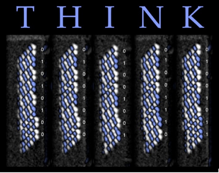
Punctuating 30 years of nanotechnology research, scientists from IBM Research (NYSE: IBM) have successfully demonstrated the ability to store information in as few as 12 magnetic atoms. This is significantly less than today's disk drives, which use about one million atoms to store a single bit of information. The ability to manipulate matter by its most basic components - atom by atom - could lead to the vital understanding necessary to build smaller, faster and more energy-efficient devices.

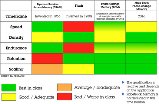
While silicon transistor technology has become cheaper, denser and more efficient, fundamental physical limitations suggest this path of conventional scaling is unsustainable. Alternative approaches are needed to continue the rapid pace of computing innovation.

Christmas Special: The PC Technology of 2011

Welcome to the TechPowerUp 2011 PC technology Christmas special. We hope that you will enjoy reading it while tucking into your turkey, Christmas presents and a little too much wine... In this article, we go through the technology of 2011 that has had the most significance, the most impact and was generally the most talked about. It's not necessarily the best tech of 2011 which is the most significant though, since lemons can be just as significant as the ground-breakers in how they fail to deliver - and the backlash that goes with it.

January: Intel Sandy Bridge i5 & i7

Released on January 9th, the new Intel Core i5 & i7 processors were based on Intel's second generation Core architecture built on a 32 nm production process (HEXUS review). They included an IGP (Integrated Graphics Processor) physically on the same piece of silicon along with HyperThreading. These new dual and quad core processors soundly beat all previous generations of Intel processors in terms of processing performance, heat, power use, features and left AMD in the dust. Therefore, Intel badly needed some competition from AMD and unless you have been living under a rock, you will know how that turned out in October with the launch of Bulldozer. Sandy Bridge was a sound win and is generally considered to be the only architecture worth considering at this point. The i5-2500K is currently at the sweet spot of price/performance. It comes at a stock speed of 3.3 GHz, but typically overclocks to an amazing 4.5 - 5 GHz with a decent air cooler and without too much difficulty in getting there. Models in the budget i3 range were released at various times later. See this Wikipedia article for details.

DDR4 May Use 3D Stacking Technology

Micron Technology, one of the biggest DRAM companies, has announced that it's working the JEDEC standards organization for computer memory, to standardize a new DRAM interface and die-stacking technology called three-dimensional stacking, or 3DS, which may be incorporated into the upcoming DDR4 standard. X-bit labs has a nice summary of how 3DS works:
The idea behind 3DS is to use specially designed and manufactured master-and-slave DRAM die, with only the master die interfacing with the external memory controller. 3DS technology uses optimized DRAM die, single DLL per stack, reduced active logic, single shared external I/O, improved timing, and reduced load to the external world. This combination of features can improve timing, bus speeds, and signal integrity while lowering both power consumption and system overhead for next-generation modules, according to Micron.

R&D: IBM's Racetrack Memory, Data Storage At Superfast DRAM Speeds

Racetrack memory, is a new type of magnetic memory that has magnetic domains "racing" along tiny nanometer sized wires, giving performance similar to conventional DRAM. Invented by IBM Fellow, Stuart Parkin, it has been in development since about 2004, with a working prototype having now been unveiled containing 256 "racetrack" cells, each containing a single wire. The technology works by sending very fast electric pulses down these wires, measured in nanoseconds, which transmit very fast moving magnetic domains which are then read by a magnetic head either as a one or a zero, depending on their direction. IBM said in a statement: "This breakthrough could lead to a new type of data-centric computing that allows massive amounts of stored information to be accessed in less than a billionth of a second."

IBM to Produce Micron's HMC in Debut of First Commercial, 3D Chip-Making Capability

IBM (NYSE: IBM) and Micron Technology, Inc. announced today that Micron will begin production of a new memory device built using the first commercial CMOS manufacturing technology to employ through-silicon vias (TSVs). IBM's advanced TSV chip-making process enables Micron's Hybrid Memory Cube (HMC) to achieve speeds 15 times faster than today's technology.

Micron's Hybrid Memory Cube features a stack of individual chips connected by vertical pipelines or "vias," shown above. IBM's new 3-D manufacturing technology, used to connect the 3D micro structure, will be the foundation for commercial production of the new memory cube.

IBM will present the details of its TSV manufacturing breakthrough at the IEEE International Electron Devices Meeting on December 5 in Washington, DC.

Workers of Supplier for Apple and IBM in China Strike

Over a thousand workers in Shenzhen, China went on strike against their employer Jingmo Electronics Corporation (JEC), which is a supplier for companies like Apple and IBM. According to China Labor Watch (CLW), a New York-based watchdog of labor rights in China, and an advocate of ethical consumerism, "the motivation behind the strike was the factory's decision to make workers work nightly overtime." CLW goes on to add that the workers had been asked to work from 6 PM to midnight and sometimes even up to 2 AM on top of the usual four to four and a half day shifts from 7 AM to 11.30 or 1 PM to 5 PM.

CLW goes on to add that the workers "commonly worked anywhere from 100 to 200 hours of overtime a month," but the factory refused to let them put the hours in at the weekend because under Chinese labour law JEC would have had to double the wages. Authorities dispatched several hundred riot policemen to tackle striking workers. CLW called upon Apple and IBM to assume responsibility of for these workers' dissatisfaction, and work with JEC to improve the working conditions in the factory. Responding to the strike, JEC agreed to cut the average overtime hours, and resume operations soon.

AMD Appoints Mark Papermaster as Senior Vice President and Chief Technology Officer

AMD (NYSE: AMD) announced today that Mark Papermaster, 50, has joined as the company's senior vice president and chief technology officer. He will report to President and Chief Executive Officer Rory Read and will oversee all of AMD's engineering, research and development (R&D), and product development functions as the head of the newly-formed Technology and Engineering Group. Papermaster, who was most recently vice president of Silicon Engineering at Cisco, will be responsible for establishing and executing the company's technology and product roadmaps, integrated hardware and software development, and overseeing the creation of all of AMD's products.

The advanced research and development team led by Senior Vice President of Research and Development Chekib Akrout, as well as the engineering teams residing in AMD's Products Group, will now report to Papermaster. Akrout, 53, will maintain responsibility for leading AMD's processor core development as well as system-on-a-chip (SoC) design methodology. In recognition of his ongoing technical and management contributions, Akrout will continue serving on AMD's senior leadership team responsible for key decision making and strategy setting.

Apple Emerges Victorious Against Psystar, But Have They Really Triumphed? (UPDATED)

In a court ruling on Wednesday 28th September 2011, Apple's assertion that any kind of 'Hackintosh' was, is and always will be, illegal, was conclusively affirmed. This will bring great dismay to Psystar customers, potential purchasers of other "alternative Macs" and the many PC enthusiasts who want to run the latest Apple OS on the high-spec rigs they've built themselves from hand-picked components. This ruling has unfortunately sounded the death knell for enterprising and surprisingly plucky upstart outfit, Psystar, who showed what could be possible with an open mind and technical skill. UPDATE after the jump.

HP Kills TouchPad, Could Spin Off PC Business

PC major HP announced its decision to scrap TouchPad, the company's flagship tablet device. But in a move that could rattle the OEM industry, there are feelers that HP might spin off its PC business. This is similar to what IBM did with its PC division, resulting in the subsequent creation of Lenovo. This move could take effect as early as by the end of this year. This is one of the most extreme makeovers in the company's 72-year history. It is sought to increase the company's long-term competitiveness against rival IBM.

It is not known if the decision to spin off the PC division will affect any of the 300,000 jobs HP maintains worldwide. HP's PC division (that sells desktop PCs, notebooks, and netbooks and related support services), is its biggest revenue generator, but also it's least profitable division. Whatever the reasoning behind this, the decision is a 180 degree turn from last decade, when HP spent no less than US $24 billion to acquire Compaq Computer, on its road to become the biggest PC vendor.

IBM Scientists Demonstrate Computer Memory Breakthrough

For the first time, scientists at IBM Research have demonstrated that a relatively new memory technology, known as phase-change memory (PCM), can reliably store multiple data bits per cell over extended periods of time. This significant improvement advances the development of low-cost, faster and more durable memory applications for consumer devices, including mobile phones and cloud storage, as well as high-performance applications, such as enterprise data storage.

With a combination of speed, endurance, non-volatility and density, PCM can enable a paradigm shift for enterprise IT and storage systems within the next five years. Scientists have long been searching for a universal, non-volatile memory technology with far superior performance than flash - today's most ubiquitous non-volatile memory technology. The benefits of such a memory technology would allow computers and servers to boot instantaneously and significantly enhance the overall performance of IT systems. A promising contender is PCM that can write and retrieve data 100 times faster than flash, enable high storage capacities and not lose data when the power is turned off. Unlike flash, PCM is also very durable and can endure at least 10 million write cycles, compared to current enterprise-class flash at 30,000 cycles or consumer-class flash at 3,000 cycles. While 3,000 cycles will out live many consumer devices, 30,000 cycles are orders of magnitude too low to be suitable for enterprise applications (see chart for comparisons).

Intel Equipped to Lead Industry to Era of Exascale Computing

At the International Supercomputing Conference (ISC), Kirk Skaugen, Intel Corporation vice president and general manager of the Data Center Group, outlined the company's vision to achieve ExaFLOP/s performance by the end of this decade. An ExaFLOP/s is quintillion computer operations per second, hundreds times more than today's fastest supercomputers.

Reaching exascale levels of performance in the future will not only require the combined efforts of industry and governments, but also approaches being pioneered by the Intel Many Integrated Core (Intel MIC) Architecture, according to Skaugen. Managing the explosive growth in the amount of data shared across the Internet, finding solutions to climate change, managing the growing costs of accessing resources such as oil and gas, and a multitude of other challenges require increased amounts of computing resources that only increasingly high-performing supercomputers can address.

IBM Microprocessors to Power the New Wii U System from Nintendo

IBM today announced that it will provide the microprocessors that will serve as the heart of the new Wii U system from Nintendo. Unveiled today at the E3 trade show, Nintendo plans for its new console to hit store shelves in 2012.

The all-new, Power-based microprocessor will pack some of IBM's most advanced technology into an energy-saving silicon package that will power Nintendo's brand new entertainment experience for consumers worldwide. IBM's unique embedded DRAM, for example, is capable of feeding the multi-core processor large chunks of data to make for a smooth entertainment experience.

IBM and Samsung Announce Joint Research into New Semiconductor Technology

IBM and Samsung today announced they will collaborate on basic research into new semiconductor materials, manufacturing processes and other technologies. The agreement calls for the two companies to jointly develop new semiconductor process technology that can be used in a broad range of applications -- from smart phone handsets to communications infrastructure.

For the first time, Samsung researchers will join IBM scientists in the Semiconductor Research Alliance at the Albany Nanotech Complex, Albany, N.Y., where researchers will investigate new materials and transistor structures, as well as innovative interconnect and packaging solutions for next-generation technology nodes. The research developments from this joint activity are planned to enable the delivery of industry leading silicon solutions that are optimized for performance, power consumption and size.

Oracle in Market for a Major Chipmaker

Oracle corporation is on a big buying spree after this year's acquisition of Sun Microsystems, a prominent server builder. Oracle wants to strengthen its enterprise IT business with the acquisition of a major chip-maker, right now AMD, IBM (its processor division), and NVIDIA are being named by prominent analysts. "You're going to see us buying chip companies," Ellison, 66, said yesterday at Oracle's annual meeting in San Francisco. Currently its subsidiary, Sun Microsystems has its own processor architecture, the SPARC. Gleacher & Co. analyst Doug Freedman predicts Oracle is chasing AMD, IBM (chip division) and NVIDIA. "You've got to think it's focused on enterprise hardware, on the server," he said. "AMD jumps off the screen."

Samsung Unveils First 16GB ‘Very Low Profile’ Module in IBM’s Newest Blade Server

Samsung Electronics Co., Ltd., the world leader in advanced memory technology, announced today that it will demonstrate for the first time a 16-Gigabyte (GB), very low profile (VLP) memory module at the VM World 2010 in an IBM H22V blade server, running on Intel Xeon 5600-series processors.

Based on 4-gigabit (Gb), 40 nanometer (nm)-class DDR3, the new modules use 18 4Gb dual-die packaged (DDP) chips, and operate on 1.35 volts of electrical current. The 16GB 40nm-class DDR3 memory provides a powerful green solution, consuming 70 percent less power than four 4GB DDR3 modules and over 40 percent less than two 8GB modules, in setting a new "standard" for lower power consumption in servers. The module's very low profile (18.75 mm high) allows it to be used in extremely compact blade servers.

Rambus Sues IBM Despite USPTO Intervention

Patent troll Rambus is at it again, this time suing IBM to reverse ruling on a memory system patent dispute after the US Patent and Trademark Office intervened in an earlier case ruling that IBM's patent 2002 memory controller-related patent applications weren't infringing on its IP. Rambus maintains that US Patent Office's ruling that gave a clean chit to IBM was in error.

In a lawsuit filed Monday in the federal court in San Jose, California, Rambus said the US Patent and Trademark Office erred through a series of decisions in finding that a patent application assigned to IBM did not interfere with its own patent obtained at the end of 2002. "The board committed errors of fact and law in its orders, decisions, and judgment," Rambus said in its complaint.

Intel Introduces 2010 Core i7 Extreme, and Most Secure Data Center Processors

Combining unprecedented security, performance and energy efficiency, Intel Corporation today launched the Intel Xeon Processor 5600 series. The new processors deliver two new security features -- Intel Advanced Encryption Standard New Instructions (Intel AES-NI), and Intel Trusted Execution Technology (Intel TXT) -- that enable faster encryption and decryption performance for more secure transactions and virtualized environments, providing data centers with a stronger foundation for cloud security.

These are also the first server and workstation chips based on the groundbreaking, new Intel 32nm logic technology, which uses Intel's second-generation high-k metal gate transistors to increase speed and decrease energy consumption. The Intel Xeon Processor 5600 series supports up to six cores per processor and delivers up to 60 percent greater performance than the 45nm Intel Xeon processor 5500 series. In addition, data centers can replace 15 single-core servers with a single new one, and achieve a return on their investment in as little as 5 months.

IBM Research Sets New Record in Magnetic Tape Data Density

IBM researchers today announced they have demonstrated a world record in areal data density on linear magnetic tape - a significant update to one of the computer industry's most resilient, reliable and affordable data storage technologies.

This breakthrough proves that tape technology can increase capacity for years to come, which has important implications, as tape storage systems are more energy efficient and cost-effective than hard disk drive storage systems. As the physical world becomes increasingly networked with sensors, vast amounts of data are amassed in various formats from medical images to security camera feeds to supply chain sensors to financial records. All of this data needs to be archived, replicated for disaster recovery, and/or retained or regulatory compliance.

NVIDIA Unveils Next Generation CUDA GPU Architecture – Codenamed ''Fermi''

NVIDIA Corp. today introduced its next generation CUDA GPU architecture, codenamed "Fermi". An entirely new ground-up design, the "Fermi" architecture is the foundation for the world's first computational graphics processing units (GPUs), delivering breakthroughs in both graphics and GPU computing.

"NVIDIA and the Fermi team have taken a giant step towards making GPUs attractive for a broader class of programs," said Dave Patterson, director Parallel Computing Research Laboratory, U.C. Berkeley and co-author of Computer Architecture: A Quantitative Approach. "I believe history will record Fermi as a significant milestone."

IBM Scientists Use DNA Scaffolding To Build Tiny Circuit Board

Today, scientists at IBM Research and the California Institute of Technology announced a scientific advancement that could be a major breakthrough in enabling the semiconductor industry to pack more power and speed into tiny computer chips, while making them more energy efficient and less expensive to manufacture.

IBM researchers and collaborator Paul W.K. Rothemund, of the California Institute of Technology, have made an advancement in combining lithographic patterning with self assembly - a method to arrange DNA origami structures on surfaces compatible with today's semiconductor manufacturing equipment.

GLOBALFOUNDRIES Breaks Ground on World's Most Advanced Semiconductor Foundry

GLOBALFOUNDRIES today announced it officially broke ground on the construction of Fab 2, a new semiconductor manufacturing facility located at the Luther Forest Technology Campus in Saratoga County, New York. Once completed, Fab 2 will stand as the most technologically advanced semiconductor manufacturing facility, or fab, in the world and the largest leading-edge semiconductor foundry in the United States. The construction and ramp-up phases for the new $4.2 billion facility are expected to take approximately three years to complete, with volume production expected in 2012.

"Semiconductors are the building blocks of technology innovation and are present in everything from mobile phones to kitchen appliances and solar panels," said Hector Ruiz, chairman of GLOBALFOUNDRIES. "As today's chip designers push the boundaries on the next generation of products, there is a growing need for a new approach to design and manufacturing rooted in collaboration and innovation. With Fab 2, GLOBALFOUNDRIES moves the semiconductor industry away from the traditional model of isolated regional development and into an era of global hubs of manufacturing and technology expertise."

IBM Launches Advanced Analytics Center in Tokyo

IBM today announced the launch of its Tokyo-based IBM Analytics Solution center which is part of a recently announced global network of analytics focused centers. Through these centers, IBM is addressing the growing demand for advanced analytics capabilities need to help clients build smarter business systems and drive improved decision-making.

The new center is co-located at IBM's Marunouchi office in Tokyo as well as at IBM's Yamato Lab in Kanagawa Prefecture. It will draw on a wealth of global IBM expertise, including more than 150 mathematicians and software engineers at IBM Research - Tokyo and Yamato Software Development Laboratory to help companies turn data into predictive intelligence. Initially, the center will be staffed by up to 500 IBM Japan consultants, researchers and software experts, with additional expertise added over time.

GLOBALFOUNDRIES Announces New Fab 2 Executive Leadership Team

GLOBALFOUNDRIES today announced the appointment of Norm Armour as vice president and general manager and Eric Choh as vice president of operations to lead an expanding team dedicated to developing Fab 2, the company's next semiconductor fabrication facility, or "fab," at the Luther Forest Technology Campus in Saratoga County, New York. Once constructed, Fab 2 is expected to be the world's most advanced semiconductor foundry, creating more than 1,200 new direct jobs plus an additional 5,000 spin-off jobs in the region.

"Norm and Eric bring a wealth of semiconductor manufacturing experience to GLOBALFOUNDRIES and will play critical leadership roles as we build and operate the most sophisticated semiconductor manufacturing facility in the world," said Douglas Grose, chief executive officer, GLOBALFOUNDRIES. "With a wealth of industry expertise in fab build-out and global operations, we now have the leadership team in place to create a cluster of semiconductor manufacturing and technology innovation in upstate New York that will bring the next wave of chip innovation to the marketplace."

GLOBALFOUNDRIES Details Advanced Technology Aimed at 22 nm and Beyond

GLOBALFOUNDRIES today described an innovative technology that could overcome one of the key hurdles to advancing high-k metal gate (HKMG) transistors, bringing the industry one step closer to the next generation of mobile devices with more computing power and vastly improved battery life.

The semiconductor industry is celebrated for overcoming seemingly insurmountable odds to continue the trend toward smaller, faster, and more energy-efficient products. Performed in partnership with IBM through GLOBALFOUNDRIES' participation in the IBM Technology Alliance, the new research is designed to enable the continued scaling of semiconductor components to the 22 nanometer node and beyond.

Intel Previews Intel Xeon 'Nehalem-EX' Processor

Intel Corporation today previewed a new Intel Xeon processor codenamed "Nehalem-EX." The processor will be at the heart of the next generation of intelligent and expandable high-end Intel server platforms, which will deliver a number of new technical advancements and boost enterprise computing performance.

In production later this year, the Nehalem-EX processor will feature up to eight cores inside a single chip supporting 16 threads and 24MB of cache. Its performance increase will be dramatic, posting the highest-ever jump from a previous generation processor.
Return to Keyword Browsing
May 21st, 2024 19:44 EDT change timezone

New Forum Posts

Popular Reviews

Controversial News Posts