News Posts matching #IEEE

Return to Keyword Browsing

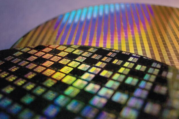
Intel, Marvell, and Synopsys to Showcase Next-Gen Memory PHY IP Capable of 224 Gbps on 3nm-class FinFET Nodes

The sneak peeks from the upcoming IEEE Solid State Circuit Conference continues, as the agenda items unveil interesting tech that will be either unveiled or demonstrated there. Intel, Synopsys, and Marvell, are leading providers of DRAM physical layer interface (PHY) IP. Various processor, GPU, and SoC manufacturers license PHY and memory controller IP from these companies, to integrate with their designs. All three companies are ready with over 200 Gbps around the 2.69 to 3 petajoule per bit range. This energy cost is as important as the data-rate on offer; as it showcases the viability of the PHY for a specific application (for example, a smartphone SoC has to conduct its memory sub-system at a vastly more constrained energy budget compared to an HPC processor).

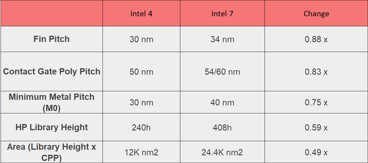
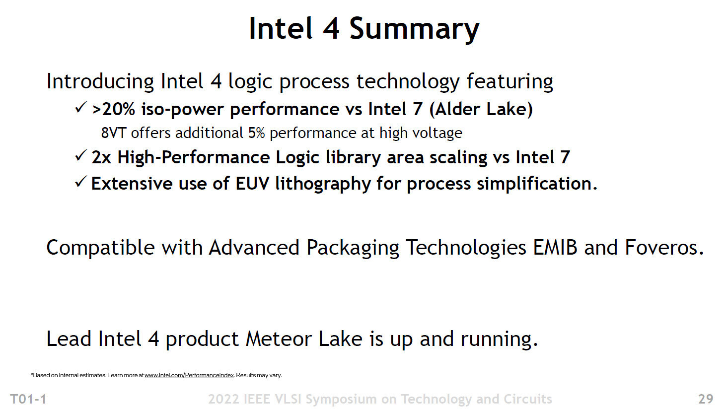
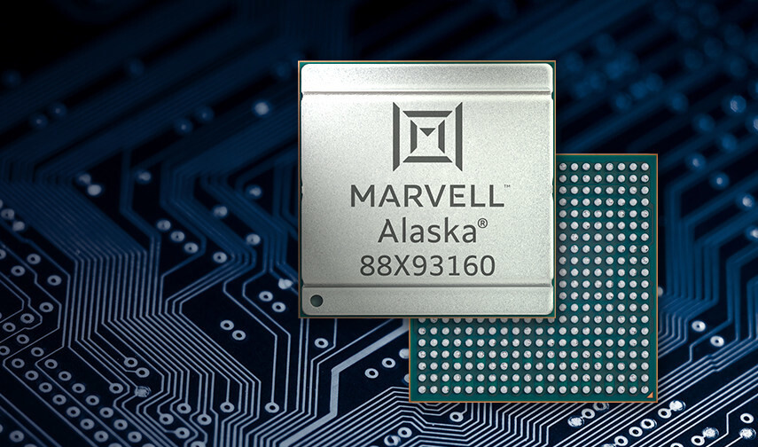
Intel is the first in the pack to showcase a 224 Gbps sub-picojoule/bit PHY transmitter that supports PAM4 and PAM6 signaling, and is designed for 3 nm-class FinFET foundry nodes. If you recall, Intel 3 will be the company's final FinFET node before it transitions to nanosheets with the Intel 20A node. At the physical layer, all digital memory signal is analogue, and Intel's IP focuses on the DAC aspect of the PHY. Next up, is a somewhat similar transceiver IP by Synopsys. This too claims 224 Gbps speeds at 3 pJ/b, but at a 40 dB insertion loss; and is designed for 3 nm class FinFET nodes such as the TSMC N3 family and Intel 3. Samsung's 3 nm node uses the incompatible GAAFET technology for its 3 nm EUV node. Lastly, there's Marvell, with a 212 Gb/s DSP-based transceiver for optical direct-detect applications on the 5 nm FinFET nodes, which is relevant for high speed network switching fabrics.

Samsung to Also Showcase 280-layer 3D QLC NAND Flash, 32 Gbit DDR5-8000 Memory Chips at IEEE-SSCC

In addition to the 37 Gbps GDDR7 memory, Samsung Electronics prepares to showcase several other memory innovations at the 2024 IEEE-SSCC as compiled by VideoCardz. To begin with, the company is showcasing a new 280-layer 3D QLC NAND flash memory in the 1 Tb density, enabling next generation of mainstream SSDs and smartphone storage. This chip offers an areal density of 28.5 Gb/mm², and a speed of 3.2 GB/s. To put this into perspective, the fastest 3D NAND flash types powering the current crop of flagship NVMe SSDs rely on 2.4 GB/s of I/O data rates.

Next up, is a new generation DDR5 memory chip offers data rates of DDR5-8000 with a density of 32 Gbit (4 GB). This chip uses a symmetric-mosaic DRAM cell architecture, and is built on a 5th generation 10 nm class foundry node Samsung optimized for DRAM products. What's impressive about this chip is that it will allow PC memory vendors to build 32 GB and 48 GB DIMMs in single-rank configuration with DDR5-8000 speeds; as well as 64 GB and 96 GB DIMMs in dual-rank configuration (impressive, provided your platform can play well with DDR5-8000 in dual-rank).

ITRI and TSMC Collaborate on Advancing High-Speed Computing with SOT-MRAM

The Industrial Technology Research Institute (ITRI) has joined forces with Taiwan Semiconductor Manufacturing Company (TSMC) for pioneering research into the development of a spin-orbit-torque magnetic random-access memory (SOT-MRAM) array chip. This SOT-MRAM array chip showcases an innovative computing in memory architecture and boasts a power consumption of merely one percent of a spin-transfer torque magnetic random-access memory (STT-MRAM) product. Their collaborative efforts have resulted in a research paper on this microelectronic component, which was jointly presented at the 2023 IEEE International Electron Devices Meeting (IEDM 2023), underscoring the cutting-edge nature of their findings and their pivotal role in advancing next-generation memory technologies.

Dr. Shih-Chieh Chang, General Director of Electronic and Optoelectronic System Research Laboratories at ITRI, highlighted the collaborative achievements of both organizations. "Following the co-authored papers presented at the Symposium on VLSI Technology and Circuits last year, we have further co-developed a SOT-MRAM unit cell," said Chang. "This unit cell achieves simultaneous low power consumption and high-speed operation, reaching speeds as rapid as 10 nanoseconds. And its overall computing performance can be further enhanced when integrated with computing in memory circuit design. Looking ahead, this technology holds the potential for applications in high-performance computing (HPC), artificial intelligence (AI), automotive chips, and more."

IBM Demonstrates a Nanosheet Transistor that Loves 77 Kelvin—Boiling Point of Nitrogen

IBM, at the 2023 IEEE International Electron Device Meeting (IEDM), demonstrated a concept nanosheet transistor that posts a near 100% performance improvement at the boiling point of nitrogen, of 77 Kelvin (-196 °C). Given how relatively industrialized and scaled out the manufacture, safe transport, storage, and use of liquid nitrogen is, this development potentially unlocks a new class of chips that attain top performance under liquid nitrogen cooling. Think a new generation of AI HPC accelerators that can instantly double their performance under LN2, provided a new kind of cooling solution is developed for data-centers.

Nanosheet transistors are the evolutionary next step to FinFETs, which have been driving semiconductor foundries since 16 nm, which could see their technical limits met at 3 nm. Nanosheets are expected to make their debut with 2 nm-class nodes such as the TSMC N2 and Intel 20A. At an operating temperature of 77 K, IBM's nanosheet device is claimed to offer a near doubling in performance, due to less charge carrier scattering, which results in lower power. Reducing scattering reduces resistance in the wires, letting electrons move through the device more quickly. Combined with lower power, devices can drive a higher current at a given voltage. Cooling also results in greater sensitivity between the device's on and off positions, so it takes lesser power to switch between the two states, resulting in lower power. This lower power means that transistor widths can be lowered, resulting in higher transistor densities, or smaller chips. As of now IBM is wrestling with a technical challenge concerning the transistor's threshold voltage, a voltage which is needed to create a conducting channel between the source and the drain.

Intel, TSMC, and Samsung, Demo CFETs at IEEE IEDM Conference, Near Doubling in Transistor Densities in Sight

Last week at the IEEE International Electron Devices Meeting, the world's top-three semiconductor foundries, TSMC, Intel (Intel Foundry Services or IFS), and Samsung Electronics, demonstrated their respective approaches to an evolutionary new transistor device called the CFET, or complementary field-effect transistors. A CFET is a kind of 3-D transistor that stacks both kinds of FETs needed for CMOS logic. All three fabs are transitioning from FinFET to nanosheets, or GAAFETs (gates all-around FETs).

While FinFETs use vertical silicon fins, with gates controlling the flow of current through them; while in a nanosheet, the vertical fin is cut into a set of ribbons, each surrounded by the gate. A CFET is essentially a taller nanosheet device in which uses half of the available ribbons for one device, and the other half for another. This device builds the two types of transistor, nFETs and pFETs on top of each other, in an integrated process. CFETs are the evolutionary next step to conventional GAAFETs, and it's predicted to enter mass production only 7-10 years from now. By that time, the industry will begin to feel the pushback from technological barriers preventing development beyond 10 angstrom-class nodes.

Intel Demos 3D Transistors, RibbonFET, and PowerVia Technologies

During the 69th annual IEEE International Electron Devices Meeting (IEDM), Intel demonstrated some of its latest transistor design and manufacturing advancements. The first one in line is the 3D integration of transistors. According to Intel, the company has successfully stacked complementary field effect transistors (CFET) at a scaled gate pitch down to 60 nm. With CFETs promising thinner gate channels, the 3D stacked CFET would allow for higher density by going vertically and horizontally. Intel's 7 node has a 54 nm gate pitch, meaning CFETs are already close to matching production-ready nodes. With more time and development, we expect to see 3D stacked CFETs in the production runs in the coming years.

Next, Intel has demonstrated RibbonFET technology, a novel approach that is the first new transistor architecture since the introduction of FinFET in 2012. Using ribbon-shaped channels surrounded by the gate, these transistors allow for better control and higher drive current at all voltage levels. This allows faster transistor switching speeds, which later lead to higher frequency and performance. The width of these nanoribbon channels can be modulated depending on the application, where low-power mobile applications use less current, making the channels thinner, and high-performance applications require more current, making the channels wider. One stack of nanoribbons can achieve the same drive current as multiple fins found in FinFET but at a smaller footprint.

QNAP Introduces the Half-width Rackmount 16-Port 10GbE QSW-M3216R-8S8T and QSW-3216R-8S8T L2 Managed/Unmanaged Switch

QNAP Systems, Inc., a leading computing, networking, and storage solutions innovator, today released the new Half-width Rackmount 16-port 10GbE switch series, including the L2 Web Managed QSW-M3216R-8S8T and the Unmanaged QSW-3216R-8S8T. The built-in eight 10GbE SFP+ and eight 10GbE RJ45 ports with backward compatibility fulfills the versatile demands of interfaces and speeds in high-speed network infrastructure. The half-width rackmount compact design also allows SMBs to flexibly deploy them in IT rooms or even on desks in offices.

"QNAP's best-selling all 10GbE switch series now releases two new half-width rackmount 16-port 10GbE models, offering more 10GbE ports to satisfy requirements for multiple high-bandwidth network devices in SMBs and offices. " said Jerry Deng, Product Manager of QNAP, adding "Managed and unmanaged models are available for easily upgrading to a full 10GbE high-speed LAN at an affordable price, and their small physical footprint makes them especially useful for businesses and organizations that lack physical space for dedicated IT hardware."

JEDEC and Open Compute Project Foundation Pave the Way for a New Era of Chiplet Innovation

In an extraordinary leap forward for the chiplet industry, the groundbreaking collaboration between the Open Compute Project Foundation (OCP) and JEDEC is set to usher in a new era of innovation. By merging the capabilities and open standards of OCP's Chiplet Data Extensible Markup Language (CDXML) and JEDEC's JEP30 PartModel Guidelines, this partnership, initiated in late 2022, promises to revolutionize chiplet design, manufacturing and integration. The result will be a unified structure that supports both chiplets and general electronic parts within the overarching purview of JEDEC.

In a significant development, the integration of OCP CDXML into JEP30 has reached a critical milestone, enabling chiplet builders to provide standardized chiplet part descriptions to their customers electronically. This advancement opens the door to automating System in Package (SiP) design and assembly using chiplets. The chiplet descriptions encompass crucial information for SiP builders, including thermal properties, physical and mechanical requirements, behavior specifications, power and signal integrity properties, testing in-package and security parameters.

Intel Launches Wi-Fi 7 Chipsets Before the Official Standard Release

Intel today updated its ARK listings with two new networking chipsets: Wi-Fi 7 BE200 and Wi-Fi 7 BE202. The company unveiled IEEE 802.11be (Wi-Fi 7) specification-based chipsets despite the standard still needing final ratification. The Wi-Fi 7 standard promises data rates as high as 40 Gbit/s, with Intel's BE200 chipset using 2x2 TX/RX streams with 2.4 GHz, 5 GHz, and 6 GHz bands. However, as demonstrated by the adapter's maximum speed of 5 Gbit/s, real-world implementations might not initially reach the theoretical maximum speed. Various motherboards, like the upcoming Gigabyte Aorus Z790 Master X, are already planning to integrate this technology, showing that the industry is getting ready for a Wi-Fi 7 world.

What makes Wi-Fi 7 especially interesting is its raw speed and underlying technology designed to improve efficiency and capacity. Features like Multi-User Multiple-Input Multiple-Output (MU-MIMO) and Orthogonal Frequency-Division Multiple Access (OFDMA), which were introduced in Wi-Fi 6 and 6E, are mandatory in Wi-Fi 7. These technologies aim to optimize the overall performance of wireless networks, making them more suitable for bandwidth-intensive tasks like AR and VR. While full certification for Wi-Fi 7 is not expected until 2024, with widespread adoption to follow, the technology looks poised to become a significant aspect of our wireless future.

LiFi 802.11bb Standard Certified by IEEE - Said to be Quicker than Wi-Fi

The Institute of Electrical and Electronics Engineers (IEEE) has certified 802.11bb as a standard for light-based wireless communications—this development was announced yesterday, and warmly received by numerous Li-Fi businesses operating around the world, including pureLiFi and Fraunhofer HHI. These organizations hope that the (currently niche market) technology will get adopted at a greater rate thanks to the IEEE's approval. Proponents of the standard proclaim that it is "faster, more reliable wireless communications with unparalleled security compared to conventional technologies such as Wi-Fi and 5G (radio frequency networks)."

pureLiFi boasts that their Light Antenna ONE module is on the cusp of being ready for mass production: "This innovative device is the result of groundbreaking work by world-renowned LiFi engineers and marks a significant milestone in the development of LiFi technology. With Light Antenna ONE, millions of people can now be connected through light, opening up a new world of possibilities for high-speed, secure, and reliable communication. The design of this cutting-edge module enables mass integration of LiFi technology for the first time, paving the way for a future where LiFi plays a crucial role in our daily lives." Sample units can be sent to OEMs for evaluation purposes—the baseband agnostic (802.11 and G.hn) EVK consists of a solderable castellated module and motherboard.

IEEE 802.11bb Global Light Communications Standard Released

Global LiFi technology firms pureLiFi and Fraunhofer HHI welcome the release of IEEE 802.11bb as the latest global light communications standard alongside IEEE 802.11 WiFi standards. The bb standard marks a significant milestone for the LiFi market, as it provides a globally recognised framework for deployment of LiFi technology.

LiFi is a wireless technology that uses light rather than radio frequencies to transmit data. By harnessing the light spectrum, LiFi can unleash faster, more reliable wireless communications with unparalleled security compared to conventional technologies such as WiFi and 5G. The Light Communications 802.11bb Task Group was formed in 2018 chaired by pureLiFi and supported by Fraunhofer HHI, two firms which have been at the forefront of LiFi development efforts. Both organisations aim to see accelerated adoption and interoperability not only between LiFi vendors but also with WiFi technologies as a result of these standardisation efforts.

Intel, Arm, and NVIDIA Propose a new 8-bit FP Format to Accelerate AI

Arm, Intel and NVIDIA have jointly authored a paper describing an 8-bit floating point (FP8) specification and its two variants E5M2 and E4M3 to provide a common interchangeable format that works for both artificial intelligence (AI) training and inference. This cross-industry specification alignment will allow AI models to operate and perform consistently across hardware platforms, accelerating AI software development.

Computational requirements for AI have been growing at an exponential rate. New innovation is required across hardware and software to deliver computational throughput needed to advance AI. One of the promising areas of research to address this growing compute gap is to reduce the numeric precision requirements for deep learning to improve memory and computational efficiencies. Reduced-precision methods exploit the inherent noise-resilient properties of deep neural networks to improve compute efficiency.

Intel 4 Process Node Detailed, Doubling Density with 20% Higher Performance

Intel's semiconductors nodes have been quite controversial with the arrival of the 10 nm design. Years in the making, the node got delayed multiple times, and only recently did the general public get the first 10 nm chips. Today, at IEEE's annual VLSI Symposium, we get more details about Intel's upcoming nodes, called Intel 4. Previously referred to as a 7 nm process, Intel 4 is the company's first node to use EUV lithography accompanied by various technologies. The first thing when a new process node is discussed is density. Compared to Intel 7, Intel 4 will double the transistor count for the same area and enable 20% higher performing transistors.

Looking at individual transistor size, the new Intel 4 node represents a very tiny piece of silicon that is even smaller than its predecessor. With a Fin Pitch of 30 nm, Contact Gate Poly Pitch of 50 nm between gates, and Minimum Metal Pitch (M0) of 50 nm, the Intel 4 transistor is significantly smaller compared to the Intel 7 cell, listed in the table below. For scaling, Intel 4 provides double the number of transistors in the same area compared to Intel 7. However, this reasoning is applied only to logic. For SRAM, the new PDK provides 0.77 area reduction, meaning that the same SoC built on Intel 7 will not be half the size of Intel 4, as SRAM plays a significant role in chip design. The Intel 7 HP library can put 80 million transistors on a square millimeter, while Intel 4 HP is capable of 160 million transistors per square millimeter.

Intel "Meteor Lake-P" SoC with 6P+8E Compute Tile Pictured

Intel's next-generation "Meteor Lake-P" mobile processor with a 6P+8E Compute Tile was shown off at the 2022 IEEE VLSI Symposium on Tech and Circuits (6 performance cores and 8 efficiency cores). We now have annotations for all four tiles, as well as a close-up die-shot of the Compute Tile. Intel also confirmed that the Compute Tile will be built on its homebrew Intel 4 silicon fabrication process, which offers over 20% iso-power performance increase versus the Intel 7 node, through extensive use of EUV lithography.

We had earlier seen a 2P+8E version of the "Meteor Lake" Compute Tile, probably from the "Meteor Lake-U" package. The larger 6P+8E Compute tile features six "Redwood Cove" performance cores, and two "Crestmont" efficiency core clusters, each with four E-cores. Assuming the L3 cache slice per P-core or E-core cluster is 2.5 MB, there has to be 20 MB of L3 cache on the compute tile. Each P-core has 2 MB of dedicated L2 cache, while each of the two E-core clusters shares 4 MB of L2 cache among four E-cores.

Intel Breakthroughs Propel Moore's Law Beyond 2025

In its relentless pursuit of Moore's Law, Intel is unveiling key packaging, transistor and quantum physics breakthroughs fundamental to advancing and accelerating computing well into the next decade. At IEEE International Electron Devices Meeting (IEDM) 2021, Intel outlined its path toward more than 10x interconnect density improvement in packaging with hybrid bonding, 30% to 50% area improvement in transistor scaling, major breakthroughs in new power and memory technologies, and new concepts in physics that may one day revolutionize computing.

"At Intel, the research and innovation necessary for advancing Moore's Law never stops. Our Components Research Group is sharing key research breakthroughs at IEDM 2021 in bringing revolutionary process and packaging technologies to meet the insatiable demand for powerful computing that our industry and society depend on. This is the result of our best scientists' and engineers' tireless work. They continue to be at the forefront of innovations for continuing Moore's Law," said Robert Chau, Intel Senior Fellow and general manager of Components Research.

NVIDIA Founder and CEO Jensen Huang to Receive Prestigious Robert N. Noyce Award

The Semiconductor Industry Association (SIA) today announced Jensen Huang, founder and CEO of NVIDIA and a trailblazer in building accelerated computing platforms, is the 2021 recipient of the industry's highest honor, the Robert N. Noyce Award. SIA presents the Noyce Award annually in recognition of a leader who has made outstanding contributions to the semiconductor industry in technology or public policy. Huang will accept the award at the SIA Awards Dinner on Nov. 18, 2021.

"Jensen Huang's extraordinary vision and tireless execution have greatly strengthened our industry, revolutionized computing, and advanced artificial intelligence," said John Neuffer, SIA president and CEO. "Jensen's accomplishments have fueled countless innovations—from gaming to scientific computing to self-driving cars—and he continues to advance technologies that will transform our industry and the world. We're pleased to recognize Jensen with the 2021 Robert N. Noyce Award for his many achievements in advancing semiconductor technology."

ASUSTOR Launches AS-T10G2 10 Gigabit Ethernet Card

The all-new AS-T10G2 is here, bringing increased efficiency and speeds to the much beloved AS-T10G. The AS-T10G2 uses the AQC-107 controller, which offers increased performance, and lower power requirements. Using the Lockerstor 16R Pro, transfer rates were found to be up to 1127 MB/s when reading and 1124 MB/s when writing. The AS-T10G2 also supports IP, TCP, UDP checksum offload to reduce CPU usage for a more efficient experience.

The AS-T10G2 is equipped with a 10 Gbps 8p8c RJ-45 Ethernet port. The AS-T10G2 supports automatic switching between all major Ethernet speeds and is compatible with four lanes of PCI Express 3.0. Pop it into an ASUSTOR NAS running ADM 4.0 or a PC to upgrade network speeds to 10-Gigabit Ethernet. The AS-T10G2 is compatible with both full-height and half-height computers, making it compatible with almost any device featuring a PCI Express slot, ensuring affordable, yet high speed networking for both homes and businesses.

Marvell Launches Industry's First 1.6T Ethernet PHY with 100G PAM4 I/Os in 5nm

Marvell today introduced the industry's first 1.6T Ethernet PHY with 100G PAM4 electrical input/outputs (I/Os) in 5nm. The demand for increased bandwidth in the data center to support massive data growth is driving the transition to 1.6T (Terabits per second) in the Ethernet backbone. 100G serial I/Os play a critical role in the cloud infrastructure to help move data across compute, networking and storage in a power-efficient manner. The new Marvell Alaska C PHY is designed to accelerate the transition to 100G serial interconnects and doubles the bandwidth speeds of the previous generation of PHYs to bring scalability for performance-critical cloud workloads and applications such as artificial intelligence and machine learning.

Marvell's 1.6T Ethernet PHY solution, the 88X93160, enables next-generation 100G serial-based 400G and 800G Ethernet links for high-density switches. The doubling of the signaling rate creates signal integrity challenges, driving the need for retimer devices for high port count switch designs. It's critical that retimer and gearboxes used for these applications are extremely power efficient. Implemented in the latest 5nm node, the Marvell 800GbE PHY provides a 40% savings in I/O power compared to existing 50G PAM4 based I/Os.

Two New Security Vulnerabilities to Affect AMD EPYC Processors

AMD processors have been very good at the field of security, on par with its main competitor, Intel. However, from time to time, researchers find new ways of exploiting a security layer and making it vulnerable to all kinds of attacks. Today, we have information that two new research papers are being published at this year's 15th IEEE Workshop on Offensive Technologies (WOOT'21) happening on May 27th. Both papers are impacting AMD processor security, specifically, they show how AMD's Secure Encrypted Virtualization (SEV) is compromised. Researchers from the Technical University of Munich and the University of Lübeck are going to present their papers on CVE-2020-12967 and CVE-2021-26311, respectfully.

While we do not know exact details of these vulnerabilities until papers are presented, we know exactly which processors are affected. As SEV is an enterprise feature, AMD's EPYC lineup is the main target of these two new exploits. AMD says that affected processors are all of the EPYC embedded CPUs and the first, second, and third generation of regular EPYC processors. For third-generation EPYC CPUs, AMD has provided mitigation in SEV-SNP, which can be enabled. For prior generations, the solution is to follow best security practices and try to avoid an exploit.
AMD EPYC Processor

SK Hynix Envisions the Future: 600-Layer 3D NAND and EUV-made DRAM

On March 22nd, the CEO of SK Hynix, Seok-Hee Lee, gave a keynote speech to the IEEE International Reliability Physics Symposium (IRPS) and shared with experts a part of its plan for the future of SK Hynix products. The CEO took the stage and delivered some conceptual technologies that the company is working on right now. At the center of the show, two distinct products stood out - 3D NAND and DRAM. So far, the company has believed that its 3D NAND scaling was very limited and that it can push up to 500 layers sometime in the future before the limit is reached. However, according to the latest research, SK Hynix will be able to produce 600-layer 3D NAND technology in the distant future.

So far, the company has managed to manufacture and sample 512Gb 176-layer 3D NAND chips, so the 600-layer solutions are still far away. Nonetheless, it is a possibility that we are looking at. Before we reach that layer number, there are various problems needed to be solved so the technology can work. According to SK Hynix, "the company introduced the atomic layer deposition (ALD) technology to further improve the cell property of efficiently storing electric charges and exporting them when needed, while developing technology to maintain uniform electric charges over a certain amount through the innovation of dielectric materials. In addition to this, to solve film stress issues, the mechanical stress levels of films is controlled and the cell oxide-nitride (ON) material is being optimized. To deal with the interference phenomenon between cells and charge loss that occur when more cells are stacked at a limited height, SK Hynix developed the isolated-charge trap nitride (isolated-CTN) structure to enhance reliability."

QNAP Launches the QHora-301W Next-Generation Wi-Fi 6 and 10GbE Dual-port SD-WAN Router

QNAP Systems, Inc. (QNAP), a leading computing, networking, and storage solution innovator, today released the QHora-301W, a Software-Defined Wide-Area Network (SD-WAN) Router with Wi-Fi 6 and dual 10 GbE ports. This next-generation router provides not only remote multi-site VPN and complete connectivity, but also QuWAN Cloud Orchestrator topology and enhanced security features, providing a flexible and reliable high-efficiency network structure for remote working and multi-site businesses.

With an enterprise-grade Qualcomm Quad-core 2.20 GHz processor and 1 GB RAM, the QHora-301W provides high-performance Wi-Fi 6 (802.11ax) and 2.4 GHz/5 GHz dual-band wireless transmission. With eight antennas and MU-MIMO, the QHora-301W provides the perfect wireless pattern views to enhance Wi-Fi coverage signals, delivering up to 3600 Mbps transfer speed and allowing for more concurrent Wi-Fi clients. With two 10 GbE ports and four Gigabit ports, the QHora-301W offers flexible WAN/LAN configurations for optimized network deployment, achieving high-speed LAN, streamlined cross-site file transfer and auto mesh multi-site VPN. Furthermore, the QHora-301W enables interconnected Mesh VPN topology via QuWAN (QNAP's SD-WAN technology), providing reliable network infrastructure for digital transmission, prioritized network bandwidth, automatic WAN failover and centralized cloud management.

Marvell Launches a Vast Lineup of Networking PHYs: 2.5GbE, 5GbE, 10GbE, and Up

Marvell today announced an integrated set of access, aggregation and core Ethernet switch and PHY solutions that intelligently enable secure and efficient data movement throughout enterprise networks. The new portfolio is purpose-built to address the specific requirements of the borderless enterprise as mobility and cloud applications extend the boundaries of the traditional campus environment. Today's enterprise IT organizations are tasked with delivering a seamless experience - including to an ever-growing remote workforce - with zero-downtime, higher bandwidth performance for video and content sharing, and data protection and security. Marvell's unified Prestera Ethernet switch and Alaska PHY solution set is architected from the ground up with insightful telemetry, flow-aware intelligence, scalable performance and advanced integrated security technologies that set the bar in switching.

With a complete line of GE, 2.5GE, 5GE, 10GE, 25GE, 100GE and 400GE platforms, the portfolio is designed to fit a variety of network architectures at different speeds, densities and scales at small, medium and large enterprise IT organizations. This latest generation of solutions, comprised of four cutting-edge Prestera Ethernet switches and corresponding Alaska Ethernet PHYs, create a clear path to upgrade enterprise networks to multi-gigabit Ethernet in support of Wi-Fi 6 and 5G deployments. Marvell's intelligent workload management enables optimized data processing at or near the network access edge, improving the performance of hybrid cloud architectures. Insightful telemetry capabilities enable the solution to produce data that facilitates network automation and expedites forensic analytics. Advanced security features underpin trustworthiness and provide network embedded protection from ever-evolving security threats. To support emerging use cases in retail, manufacturing, hospitality, finance and education, Marvell's switching family is built with flexibility and feature richness to address the imminent needs these networks face.

Ethernet Technology Consortium Announces 800 Gigabit Ethernet (GbE) Specification

The 25 Gigabit Ethernet Consortium, originally established to develop 25, 50 and 100 Gbps Ethernet specifications, announced today it has changed its name to the Ethernet Technology Consortium in order to reflect a new focus on higher-speed Ethernet technologies.

The goal of the consortium is to enhance the Ethernet specification to operate at new speeds by utilizing specifications that are developed or in development. This allows the organization to work alongside other industry groups and standards bodies to adapt Ethernet at a pace that aligns with the rapidly evolving needs of the industry. The ETC has more than 45 members with top-level promoter members that include Arista, Broadcom, Cisco, Dell, Google, Mellanox and Microsoft.

AMD Gives Itself Massive Cost-cutting Headroom with the Chiplet Design

At its 2020 IEEE ISSCC keynote, AMD presented two slides that detail the extent of cost savings yielded by its bold decision to embrace the MCM (multi-chip module) approach to not just its enterprise and HEDT processors, but also its mainstream desktop ones. By confining only those components that tangibly benefit from cutting-edge silicon fabrication processes, namely the CPU cores, while letting other components sit on relatively inexpensive 12 nm, AMD is able to maximize its 7 nm foundry allocation, by making it produce small 8-core CCDs (CPU complex dies), which add up to AMD's target core-counts. With this approach, AMD is able to cram up to 16 cores onto its AM4 desktop socket using two chiplets, and up to 64 cores using eight chiplets on its SP3r3 and sTRX4 sockets.

In the slides below, AMD compares the cost of its current 7 nm + 12 nm MCM approach to a hypothetical monolithic die it would have had to build on 7 nm (including the I/O components). The slides suggest that the cost of a single-chiplet "Matisse" MCM (eg: Ryzen 7 3700X) is about 40% less than that of the double-chiplet "Matisse" (eg: Ryzen 9 3950X). Had AMD opted to build a monolithic 7 nm die that had 8 cores and all the I/O components of the I/O die, such a die would cost roughly 50% more than the current 1x CCD + IOD solution. On the other hand, a monolithic 7 nm die with 16 cores and I/O components would cost 125% more. AMD hence enjoys a massive headroom for cost-cutting. Prices of the flagship 3950X can be close to halved (from its current $749 MSRP), and AMD can turn up the heat on Intel's upcoming Core i9-10900K by significantly lowering price of its 12-core 3900X from its current $499 MSRP. The company will also enjoy more price-cutting headroom for its 6-core Ryzen 5 SKUs than it did with previous-generation Ryzen 5 parts based on monolithic dies.

Intel's Process Roadmap Gets Updated with Plans to go Back to Two Year Cadence

During the IEDM event hosted by the IEEE organization, ASML's CEO, Martin van den Brink, took the stage to elaborate more on ASML's vision of the future of semiconductors. When talking about the future of semiconductors, Mr. Brink started talking about Intel and their vision for the future. Intel's slides were showing many things including backporting of IP to older processes and plan to go back to "tick-tock" two-year cadence to restore the previous confidence in Intel's manufacturing capabilities.

Perhaps one of the most interesting notes about the presentation is the fact that Intel is working hard to realize its plans of bringing back a two-year cadence of "tick-tock" process realization. That means that in the future, presumably after 10 nm debut problems are solved, Intel wants to do the old process and optimization tactics. A slide (shown below) titled "In Moore We Trust" is speaking a lot about Intel's future plans, showing few things in particular: Intel's upcoming 10 nm++ and 10 nm+++ nodes, and the possibility of backporting.
Return to Keyword Browsing
May 1st, 2024 01:49 EDT change timezone

New Forum Posts

Popular Reviews

Controversial News Posts