News Posts matching #Intel 4

Return to Keyword Browsing

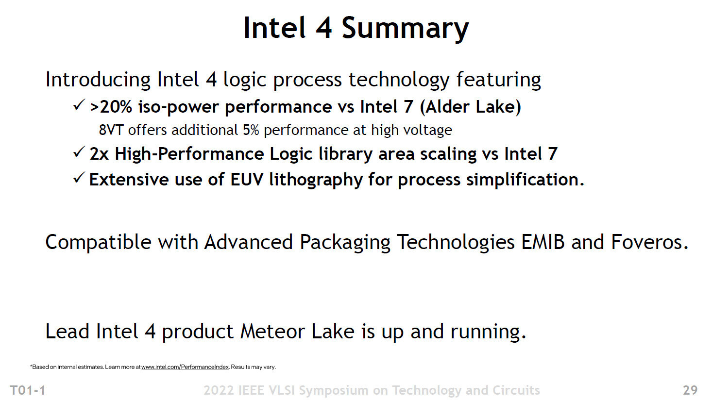
Intel 4 Process Node Detailed, Doubling Density with 20% Higher Performance

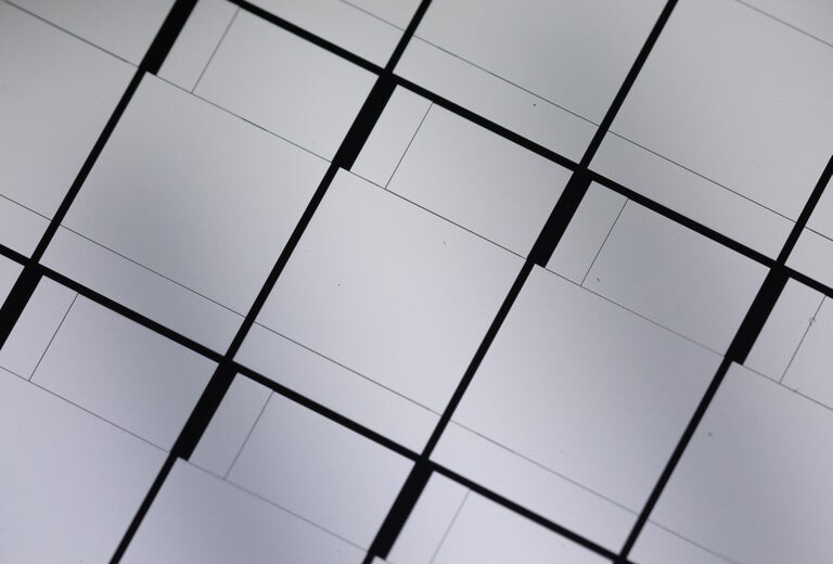
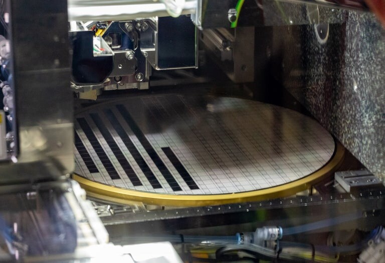
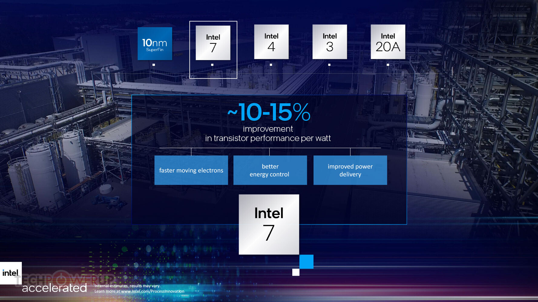
Intel's semiconductors nodes have been quite controversial with the arrival of the 10 nm design. Years in the making, the node got delayed multiple times, and only recently did the general public get the first 10 nm chips. Today, at IEEE's annual VLSI Symposium, we get more details about Intel's upcoming nodes, called Intel 4. Previously referred to as a 7 nm process, Intel 4 is the company's first node to use EUV lithography accompanied by various technologies. The first thing when a new process node is discussed is density. Compared to Intel 7, Intel 4 will double the transistor count for the same area and enable 20% higher performing transistors.

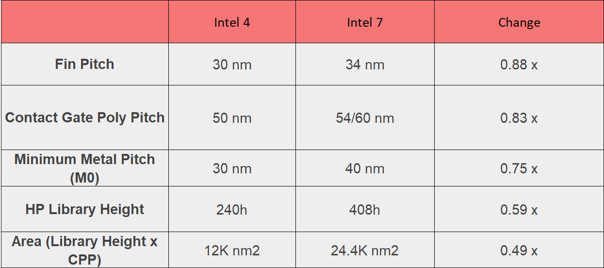
Looking at individual transistor size, the new Intel 4 node represents a very tiny piece of silicon that is even smaller than its predecessor. With a Fin Pitch of 30 nm, Contact Gate Poly Pitch of 50 nm between gates, and Minimum Metal Pitch (M0) of 50 nm, the Intel 4 transistor is significantly smaller compared to the Intel 7 cell, listed in the table below. For scaling, Intel 4 provides double the number of transistors in the same area compared to Intel 7. However, this reasoning is applied only to logic. For SRAM, the new PDK provides 0.77 area reduction, meaning that the same SoC built on Intel 7 will not be half the size of Intel 4, as SRAM plays a significant role in chip design. The Intel 7 HP library can put 80 million transistors on a square millimeter, while Intel 4 HP is capable of 160 million transistors per square millimeter.

Intel "Meteor Lake-P" SoC with 6P+8E Compute Tile Pictured

Intel's next-generation "Meteor Lake-P" mobile processor with a 6P+8E Compute Tile was shown off at the 2022 IEEE VLSI Symposium on Tech and Circuits (6 performance cores and 8 efficiency cores). We now have annotations for all four tiles, as well as a close-up die-shot of the Compute Tile. Intel also confirmed that the Compute Tile will be built on its homebrew Intel 4 silicon fabrication process, which offers over 20% iso-power performance increase versus the Intel 7 node, through extensive use of EUV lithography.

We had earlier seen a 2P+8E version of the "Meteor Lake" Compute Tile, probably from the "Meteor Lake-U" package. The larger 6P+8E Compute tile features six "Redwood Cove" performance cores, and two "Crestmont" efficiency core clusters, each with four E-cores. Assuming the L3 cache slice per P-core or E-core cluster is 2.5 MB, there has to be 20 MB of L3 cache on the compute tile. Each P-core has 2 MB of dedicated L2 cache, while each of the two E-core clusters shares 4 MB of L2 cache among four E-cores.

Intel "Meteor Lake" 2P+8E Silicon Annotated

Le Comptoir du Hardware scored a die-shot of a 2P+8E core variant of the "Meteor Lake" compute tile, and Locuza annotated it. "Meteor Lake" will be Intel's first processor to implement the company's IDM 2.0 strategy to the fullest. The processor is a multi-chip module of various tiles (chiplets), each with a certain function, sitting on die made on a silicon fabrication node most suitable to that function. Under this strategy, for example, if Intel's chip-designers calculate that the iGPU will be the most power-hungry component on the processor, followed by the CPU cores, the graphics tile will be built on a more advanced process than the compute tile. Intel's "Meteor Lake" and "Arrow Lake" processors will implement chiplets built on the Intel 4, TSMC N3, and Intel 20A fabrication nodes, each with unique power and transistor-density characteristics. Learn more about the "Meteor Lake" MCM in our older article.

The 2P+8E (2 performance cores + 8 efficiency cores) compute tile is one among many variants of compute tiles Intel will develop for the various SKUs making up the next-generation Core mobile processor series. The die is annotated with the two large "Redwood Cove" P-cores and their cache slices taking up about 35% of the die area; and the two "Crestmount" E-core clusters (each with 4 E-cores), and their cache slices, taking up the rest. The two P-cores and two E-core clusters are interconnected by a Ring Bus, and share an L3 cache. The size of each L3 cache slice is either 2.5 MB or 3 MB. At 2.5 MB, the total L3 cache will be 10 MB, and at 3 MB, it will be 12 MB. As with all past generations, the L3 cache is fully accessible by all CPU cores in the compute tile.

Intel Installs First EUV Tool in Irish Fab 34

Last week Intel finalised the installation of its first EUV tool in Fab 34, which is located in Leixlip, Ireland. That comes just two months after Intel started installing its first chipmaking equipment in the fab. The EUV tool is made by ASML, but was shipped to Intel in Hillsboro, Oregon, USA first, before being sent back to Europe. It's unclear why it was shipped to the US first, but it's possible that Intel tested the equipment there and made sure it was to its spec, before shipping it to its new fab.

This is the first of several machines from ASML that are expected to be installed in Fab 34 and Intel says it's "a key enabler of Intel 4 process technology". The ASML machine required four unspecified Boeing aircrafts to ship, as well as 35 trucks to bring it to Fab 34. The machine, or tool as Intel calls it, has been sent in parts since December last year and has only now been completely assembled. For more details, see the video after the break.

Intel "Meteor Lake" and "Arrow Lake" Use GPU Chiplets

Intel's upcoming "Meteor Lake" and "Arrow Lake" client mobile processors introduce an interesting twist to the chiplet concept. Earlier represented in vague-looking IP blocks, new artistic impressions of the chip put out by Intel shed light on a 3-die approach not unlike the Ryzen "Vermeer" MCM that has up to two CPU core dies (CCDs) talking to a cIOD (client IO die), which handles all the SoC connectivity; Intel's design has one major difference, and that's integrated graphics. Apparently, Intel's MCM uses a GPU die sitting next to the CPU core die, and the I/O (SoC) die. Intel likes to call its chiplets "tiles," and so we'll go with that.

The Graphics tile, CPU tile, and the SoC or I/O tile, are built on three different silicon fabrication process nodes based on the degree of need for the newer process node. The nodes used are Intel 4 (optically 7 nm EUV, but with characteristics of a 5 nm-class node); Intel 20A (characteristics of 2 nm), and external TSMC N3 (3 nm) node. At this point we don't know which tile gets what. From the looks of it, the CPU tile has a hybrid CPU core architecture made up of "Redwood Cove" P-cores, and "Crestmont" E-core clusters.

Intel Updates Technology Roadmap with Data Center Processors and Game Streaming Service

At Intel's 2022 Investor Meeting, Chief Executive Officer Pat Gelsinger and Intel's business leaders outlined key elements of the company's strategy and path for long-term growth. Intel's long-term plans will capitalize on transformative growth during an era of unprecedented demand for semiconductors. Among the presentations, Intel announced product roadmaps across its major business units and key execution milestones, including: Accelerated Computing Systems and Graphics, Intel Foundry Services, Software and Advanced Technology, Network and Edge, Technology Development, More: For more from Intel's Investor Meeting 2022, including the presentations and news, please visit the Intel Newsroom and Intel.com's Investor Meeting site.

SiFive Partners with Intel to Spark Innovation in High-Performance RISC-V Platforms

SiFive, Inc., the founder and leader of RISC-V computing, today announced the company will support Intel Foundry Services (IFS) innovation fund's goal to build innovative new RISC-V computing platforms optimized for Intel process technology. The $1B Intel fund will support the creation of disruptive technologies to address modern computing challenges, with the Intel-SiFive collaboration aiming to extend the RISC-V ecosystem. Compute blocks in future silicon chips, optimized for specific classes of workloads, require a vibrant market of semiconductor IP that is further enabled by SiFive's leading RISC-V processor IP optimized and available to customers of IFS. The open nature of the RISC-V instruction set architecture creates freedom to innovate, with specifications and extensions developed by expert contributors from leaders in the semiconductor industry, research institutions, and academia.

SiFive has partnered with IFS to develop a RISC-V development platform, codenamed "Horse Creek," featuring a multi-core SiFive Performance P550 processor, and implemented on the Intel 4 technology platform, on track for availability in 2022. The "Horse Creek" SoC will enable a new generation of RISC-V developer boards, continuing the tradition of SiFive HiFive boards that have helped drive the growth of the RISC-V ecosystem. To be informed of updates on the "Horse Creek" RISC-V developer board, please register here.

Intel Ireland Fab 34 Achieves Development Milestone, Facility to Drive Intel 4 Node

Intel Ireland last week chalked up a milestone in its $7 billion Fab 34 construction project: A team rolled in the new plant's first huge chipmaking tool. The machine, a lithography resist track, arrived by truck at Intel's Leixlip, Ireland, plant after a flight across the Atlantic Ocean from an Intel Oregon plant.

Ireland's new lithography tool runs in conjunction with an extreme ultraviolet (EUV) scanner, a crown jewel in Intel's manufacturing capability. The new tool provides precision coating of silicon wafers before alignment and exposure inside the EUV scanner. The wafer then returns to the lithography tool for a series of precision oven bakes, photo development and rinsing. A typical Intel fab contains about 1,200 advanced tools, many of them costing millions of dollars a piece.

Intel "Meteor Lake" Chips Already Being Built at the Arizona Fab

With its 12th Gen Core "Alder Lake-P" mobile processors still on the horizon, Intel is already building test batches of the 14th Gen "Meteor Lake" mobile processors, at its Fab 42 facility in Chandler, Arizona. "Meteor Lake" is a multi-chip module that leverages Intel's Foveros packaging technology to combine "tiles" (purpose built dies) based on different silicon fabrication processes depending on their function and transistor-density/power requirements. It combines four distinct tiles across a single package—the compute tile, with the CPU cores; the graphics tile with the iGPU: the SoC I/O tile, which handles the processor's platform I/O; and a fourth tile, which is currently unknown. This could be a memory stack with similar functions as the HBM stacks on "Sapphire Rapids," or something entirely different.

The compute tile contains the processor's various CPU core types. The P cores are "Redwood Cove," which are two generations ahead of the current "Golden Cove." If Intel's 12-20% generational IPC uplift cadence holds, we're looking at cores with up to 30% higher IPC than "Golden Cove" (50-60% higher than "Skylake."). "Meteor Lake" also debuts Intel's next-generation E-core, codenamed "Crestmont." The compute tile is rumored to be fabricated on the Intel 4 node (optically a 7 nm-class node, but with characteristics similar to TSMC N5).

Intel Advances Neuromorphic with Loihi 2, New Lava Software Framework and New Partners

Today, Intel introduced Loihi 2, its second-generation neuromorphic research chip, and Lava, an open-source software framework for developing neuro-inspired applications. Their introduction signals Intel's ongoing progress in advancing neuromorphic technology. Neuromorphic computing, which draws insights from neuroscience to create chips that function more like the biological brain, aspires to deliver orders of magnitude improvements in energy efficiency, speed of computation and efficiency of learning across a range of edge applications: from vision, voice and gesture recognition to search retrieval, robotics, and constrained optimization problems.

"Loihi 2 and Lava harvest insights from several years of collaborative research using Loihi. Our second-generation chip greatly improves the speed, programmability, and capacity of neuromorphic processing, broadening its usages in power and latency constrained intelligent computing applications. We are open sourcing Lava to address the need for software convergence, benchmarking, and cross-platform collaboration in the field, and to accelerate our progress toward commercial viability." -- Mike Davies, director of Intel's

Intel Expects New US Fab Investment to Cost $60 to $120 billion

In an interview with the Washington Post, Intel CEO Pat Gelsinger shared some details on the company's plans to expand its foundry operations in the US. As part of the company's IDM 2.0 plan, the company aims to construct a new cutting edge fabrication complex that will cover both wafer manufacturing and advanced packaging technologies. While the final factory location still hasn't been disclosed, the company said it plans to build the complex in close proximity to universities - a way to facilitate the hiring process of qualified personnel and, perhaps, of establishing joint research and development. Intel expects this foundry complex to cost between $60 and $120 billion.
Intel CEO Pat GelsingerWe are looking broadly across the U.S.. This would be a very large site, so six to eight fab modules, and at each of those fab modules, between 10- and $15 billion. It's a project over the next decade on the order of $100 billion of capital, 10,000 direct jobs. 100,000 jobs are created as a result of those 10,000, by our experience. So, essentially, we want to build a little city."

Intel Rebadges 10nm Enhanced SuperFin Node as "Intel 7," Invents Other Creative Node Names

Intel, in a move comparable to its competitors' Performance Rating system from the 1990s, has invented a new naming scheme for its in-house foundry nodes to claim technological parity with contemporaries such as TSMC and Samsung, that are well into the sub-10 nm class. Back in the i586 era, when Intel's competitors such as AMD and Cyrix, couldn't keep up with its clock-speeds yet found their chips to be somewhat competitive, they invented the PR (processor rating) system, with a logical number attempting to denote parity with an Intel processor's clock-speed. For example, a PR400 processor rating meant that the chip rivaled a Pentium II 400 MHz (which it mostly didn't). The last that the PR system made sense was with the final generation of single-core performance chips, Pentium 4 and Athlon XP, beyond which, the introduction of multi-core obfuscated the PR system. A Phenom X4 9600 processor didn't mean performance on par with a rival Intel chip running at an impossible 9.60 GHz.

Intel's new foundry naming system sees its 10 nm Enhanced SuperFin node re-badge as "Intel 7." The company currently builds 11th Gen Core "Tiger Lake" processors on the 10 nm SuperFin node, and is expected to build its upcoming 12th Gen Core "Alder Lake" chips on its refinement, the 10 nm Enhanced SuperFin, which will now be referred to as "Intel 7." The company is careful to avoid using the nanometer unit next to the number, instead signaling the consumer that the node somehow offers transistor density and power characteristics comparable to a 7 nm node. Intel 7 offers a 10-15 percent performance/Watt gain over 10 nm SuperFin, and is already in volume production, with a debut within 2021 with "Alder Lake."

Intel Accelerates Packaging and Process Innovations

Intel Corporation today revealed one of the most detailed process and packaging technology roadmaps the company has ever provided, showcasing a series of foundational innovations that will power products through 2025 and beyond. In addition to announcing RibbonFET, its first new transistor architecture in more than a decade, and PowerVia, an industry-first new backside power delivery method, the company highlighted its planned swift adoption of next-generation extreme ultraviolet lithography (EUV), referred to as High Numerical Aperture (High NA) EUV. Intel is positioned to receive the first High NA EUV production tool in the industry.

"Building on Intel's unquestioned leadership in advanced packaging, we are accelerating our innovation roadmap to ensure we are on a clear path to process performance leadership by 2025," Intel CEO Pat Gelsinger said during the global "Intel Accelerated" webcast. "We are leveraging our unparalleled pipeline of innovation to deliver technology advances from the transistor up to the system level. Until the periodic table is exhausted, we will be relentless in our pursuit of Moore's Law and our path to innovate with the magic of silicon."
Return to Keyword Browsing
May 21st, 2024 22:30 EDT change timezone

New Forum Posts

Popular Reviews

Controversial News Posts