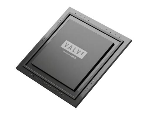
Valve Steam Deck SoC Detailed: AMD Brings Zen2 and RDNA2 to the Table
Valve today announced its first big splash into the console market with Steam Deck, a device out to eat the Nintendo Switch's lunch. The announcement comes as yet another feather in AMD's cap for its semi-custom SoC business, benefiting from being the only company with an x86-64 CPU license and having a cutting-edge graphics hardware IP. Built on the 7 nm node at TSMC, the semi-custom chip at the heart of the Steam Deck is designed for extended gameplay on battery, and is a monolithic silicon that combines CPU, GPU, and core-logic.
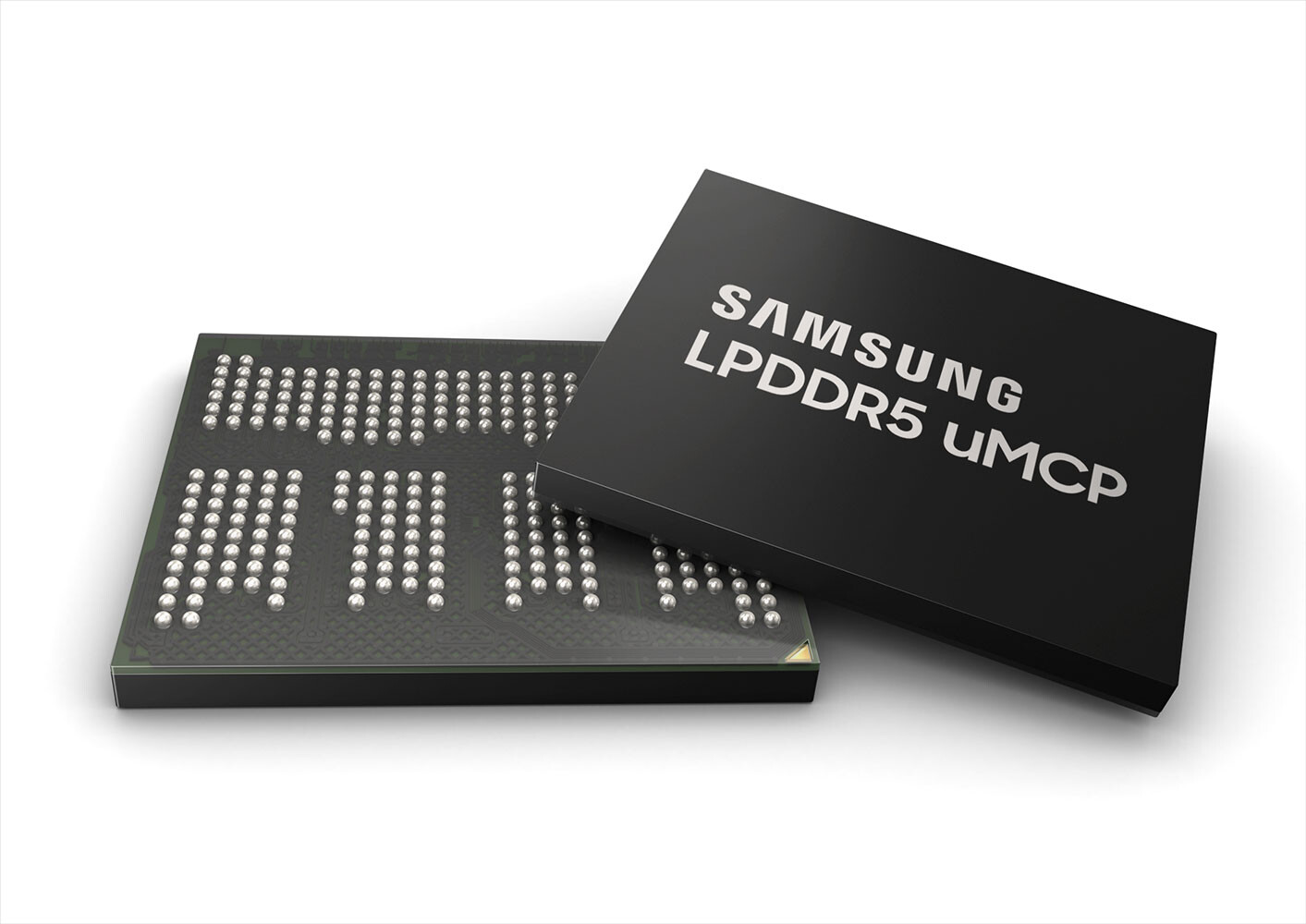
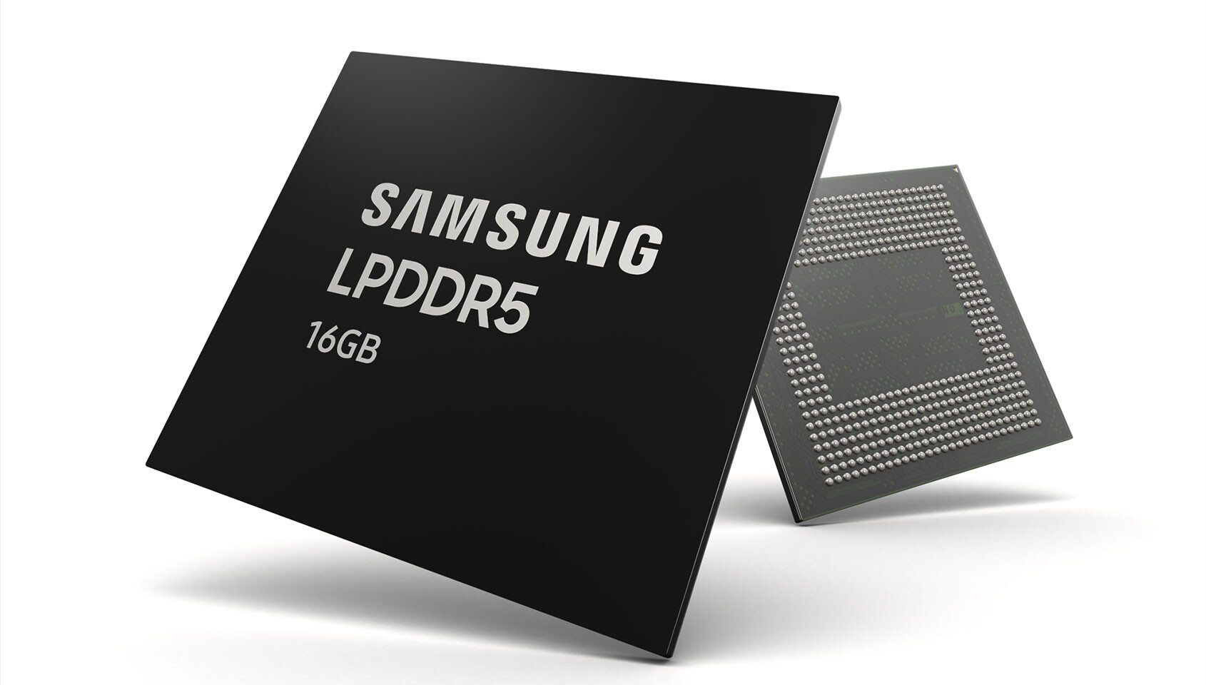
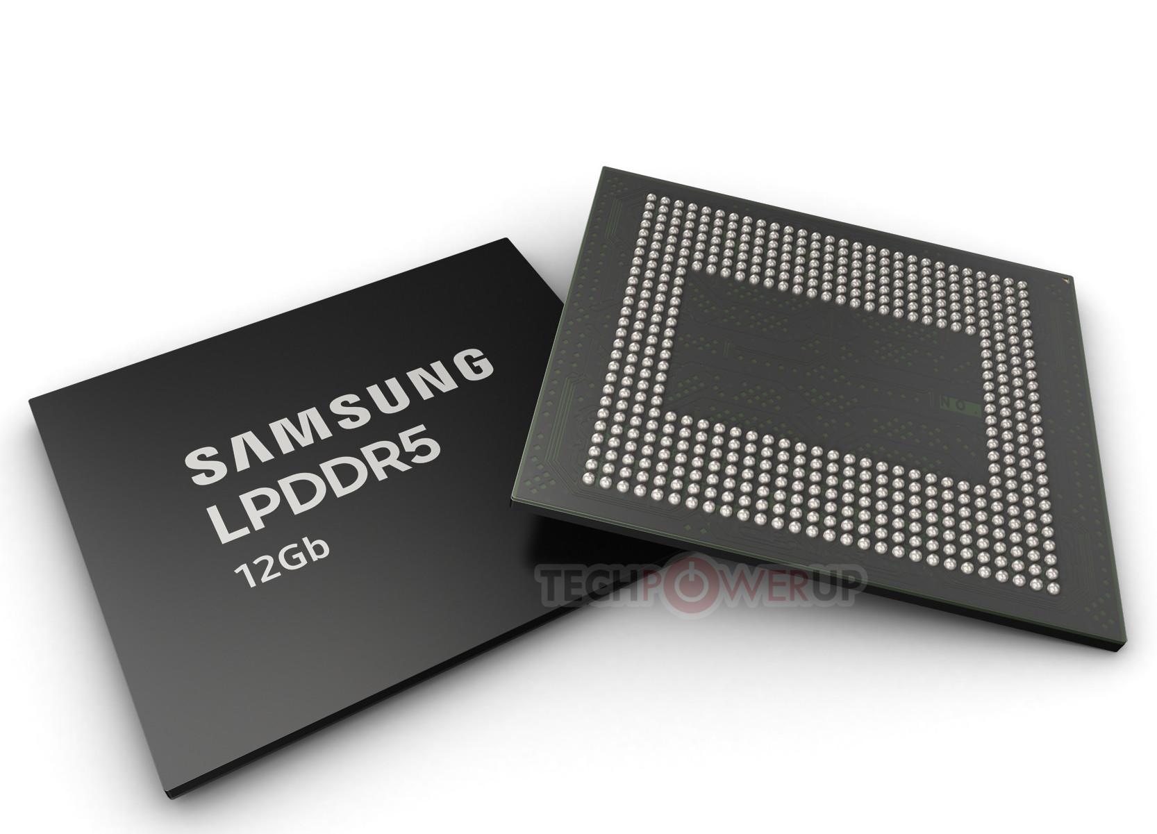
The yet-unnamed semi-custom chip features a 4-core/8-thread CPU based on the "Zen 2" microarchitecture, with a nominal clock speed of 2.40 GHz, and up to 3.50 GHz boost. The CPU component offers an FP32 throughput of 448 GFLOP/s. The GPU is based on AMD's latest RDNA2 graphics architecture—the same one powering the Xbox Series X, PlayStation 5, and Radeon RX 6900 XT—and is comprised of 8 RDNA2 compute units (512 stream processors). The GPU operates at an engine clock speed of 1.10 GHz to 1.60 GHz, with peak compute power of 1.6 TFLOP/s. The silicon uses a unified memory interface, and a cutting-edge LPDDR5 memory controller.

The yet-unnamed semi-custom chip features a 4-core/8-thread CPU based on the "Zen 2" microarchitecture, with a nominal clock speed of 2.40 GHz, and up to 3.50 GHz boost. The CPU component offers an FP32 throughput of 448 GFLOP/s. The GPU is based on AMD's latest RDNA2 graphics architecture—the same one powering the Xbox Series X, PlayStation 5, and Radeon RX 6900 XT—and is comprised of 8 RDNA2 compute units (512 stream processors). The GPU operates at an engine clock speed of 1.10 GHz to 1.60 GHz, with peak compute power of 1.6 TFLOP/s. The silicon uses a unified memory interface, and a cutting-edge LPDDR5 memory controller.