News Posts matching #Manufacturing

Return to Keyword Browsing

US Backs TSMC's $65B Arizona Investment with $11.6B Support Package

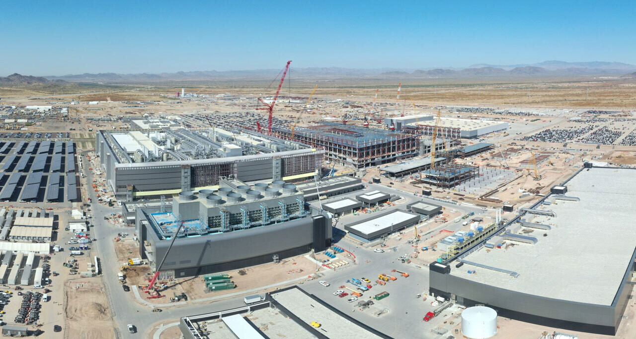
According to the latest report from Bloomberg, the US government under Joe Biden's administration has announced plans to provide Taiwan Semiconductor Manufacturing Company (TSMC) with a substantial financial support package worth $11.6 billion. The package is composed of $6.6 billion in grants and up to $5 billion in loans. This represents the most significant financial assistance approved under the CHIPS and Science Act, a key initiative to resurrect the US chip industry. The funding will aid TSMC in establishing three cutting-edge semiconductor production facilities in Arizona, with the company's total investment in the state expected to exceed an impressive $65 billion. TSMC's multi-phase Arizona project will commence with the construction of a fab module near its existing Fab 21 facility. Production using 4 nm and 5 nm process nodes is slated to begin by early 2025. The second phase, scheduled for 2028, will focus on even more advanced 2 nm and 3 nm technologies.

TSMC has kept details about the third facility's production timeline and process node under wraps. The company's massive investment in Arizona is expected to profoundly impact the local economy, creating 6,000 high-tech manufacturing jobs and over 20,000 construction positions. Moreover, $50 million has been earmarked for training local workers, which aligns with President Joe Biden's goal of bolstering domestic manufacturing and technological independence. However, TSMC's Arizona projects have encountered obstacles, including labor disputes and uncertainties regarding government support, resulting in delays for the second facility's production timeline. Additionally, reports suggest that at least one TSMC supplier has abandoned plans to set up operations in Arizona due to workforce-related challenges.

Huawei and SMIC Prepare Quadruple Semiconductor Patterning for 5 nm Production

According to Bloomberg's latest investigation, Huawei and Semiconductor Manufacturing International Corporation (SMIC) have submitted patents on the self-aligned quadruple patterning (SAQP) pattern etching technique to enable SMIC to achieve 5 nm semiconductor production. The two Chinese giants have been working with the Deep Ultra Violet (DUV) machinery to develop a pattern etching technique allowing SMIC to produce a node compliant with the US exporting rules while maintaining the density improvements from the previously announced 7 nm node. In the 7 nm process, SMIC most likely used self-aligned dual patterning (SADP) with DUV tools, but for the increased density of the 5 nm node, a doubling to SAQP is required. In semiconductor manufacturing, lithography tools take multiple turns to etch the design of the silicon wafer.

Especially with smaller nodes getting ever-increasing density requirements, it is becoming challenging to etch sub-10 nm designs using DUV tools. That is where Extreme Ultra Violet (EUV) tools from ASML come into play. With EUV, the wavelengths of the lithography printers are 14 times smaller than DUV, at only 13.5 nm, compared to 193 nm of ArF immersion DUV systems. This means that without EUV, SMIC has to look into alternatives like SAQP to increase the density of its nodes and, as a result, include more complications and possibly lower yields. As an example, Intel tried to use SAQP in its first 10 nm nodes to reduce reliance on EUV, which resulted in a series of delays and complications, eventually pushing Intel into EUV. While Huawei and SMIC may develop a more efficient solution for SAQP, the use of EUV is imminent as the regular DUV can not keep up with the increasing density of semiconductor nodes. Given that ASML can't ship its EUV machinery to China, Huawei is supposedly developing its own EUV machines, but will likely take a few more years to show.

US Government to Announce Massive Grant for Intel's Arizona Facility

According to the latest report by Reuters, the US government is preparing to announce a multi-billion dollar grant for Intel's chip manufacturing operations in Arizona next week, possibly worth more than $10 billion. US President Joe Biden and Commerce Secretary Gina Raimondo will make the announcement, which is part of the 2022 CHIPS and Science Act aimed at expanding US chip production and reducing dependence on China and Taiwan manufacturing. The exact amount of the grant has yet to be confirmed, but rumors suggest it could exceed $10 billion, making it the most significant award yet under the CHIPS Act. The funding will include grants and loans to bolster Intel's competitive position and support the company's US semiconductor manufacturing expansion plans. This comes as a surprise just a day after the Pentagon reportedly refused to invest $2.5 billion in Intel as a part of a secret defense grant.

Intel has been investing significantly in its US expansion, recently opening a $3.5 billion advanced packaging facility in New Mexico, supposed to create extravagant packaging technology like Foveros and EMIB. The chipmaker is also expanding its semiconductor manufacturing capacity in Arizona, with plans to build new fabs in the state. Arizona is quickly becoming a significant hub for semiconductor manufacturing in the United States. In addition to Intel's expansion, Taiwan Semiconductor Manufacturing Company (TSMC) is also building new fabs in the state, attracting supply partners to the region. CHIPS Act has a total funding capacity of $39 billion allocated for semiconductor production and $11 billion for research and development. The Intel grant will likely cover the production part, as Team Blue has been reshaping its business units with the Intel Product and Intel Foundry segments.

MICLEDI Microdisplays Raises Series A Funding to Advance Best-in-Class microLED Display Design and Manufacturing

MICLEDI Microdisplays today announced a first closing of its Series A funding round with participation from imec.xpand, PMV, imec, KBC and SFPIM demonstrating strong support for the company's value proposition and commercial and technological progress achieved in the seed round. Series A follows a significant seed round award and additional non-dilutive funding in the form of grants and other vehicles from VLAIO. This brings the company's total funding to date to nearly $30 million.

"The company's achievements during this seed round have been astounding," said Sean Lord, CEO of MICLEDI. "Our door is open to engagements with some of the world's largest and most innovative electronic product manufacturing companies, most of whom are working on their own internal development projects for augmented reality (AR) displays in such diverse use cases as smart-wearable devices and automotive HUDs. This level of total funding to date is almost unheard of for a four-year-old startup."

TSMC Customers Request Construction of Additional AI Chip Fabs

Morris Chang, TSMC's founder and semiconductor industry icon, was present at the opening ceremony of his company's new semiconductor fabrication plant in Kumamoto Prefecture, Japan. According to a Nikkei Asia article, Chang predicted that the nation will experience "a chip renaissance" during his February 24 commencement speech. The Japanese government also announced that it will supply an additional ¥732 billion ($4.86 billion) in subsidies for Taiwan Semiconductor Manufacturing Co. to expand semiconductor operations on the island of Kyūshū. Economy Minister Ken Saito stated: "TSMC is the most important partner for Japan in realizing digital transformation, and its Kumamoto factory is an important contributor for us to stably procure cutting-edge logic chips that is extremely essential for the future of industries in Japan."

Chang disclosed some interesting insights during last weekend's conference segment—according to Nikkei's report, he revealed that unnamed TSMC customers had made some outlandish requests: "They are not talking about tens of thousands of wafers. They are talking about fabs, (saying): 'We need so many fabs. We need three fabs, five fabs, 10 fabs.' Well, I can hardly believe that one." The Taiwanese chip manufacturing giant reportedly has the resources to create a new "Gigafab" within reasonable timeframes, but demands for (up to) ten new plants are extremely fanciful. Chang set expectations at a reasonable level—he predicted that demand for AI processors would lie somewhere in the middle ground: "between tens of thousands of wafers and tens of fabs." Past insider reports suggested that OpenAI has been discussing the formation of a proprietary fabrication network, with proposed investments of roughly $5 to $7 trillion. OpenAI CEO, Sam Altman, reportedly engaged in talks with notable contract chip manufacturers—The Wall Street Journal posited that TSMC would be an ideal partner.

GlobalFoundries and Biden-Harris Administration Announce CHIPS and Science Act Funding for Essential Chip Manufacturing

The U.S. Department of Commerce today announced $1.5 billion in planned direct funding for GlobalFoundries (Nasdaq: GFS) (GF) as part of the U.S. CHIPS and Science Act. This investment will enable GF to expand and create new manufacturing capacity and capabilities to securely produce more essential chips for automotive, IoT, aerospace, defense, and other vital markets.

New York-headquartered GF, celebrating its 15th year of operations, is the only U.S.-based pure play foundry with a global manufacturing footprint including facilities in the U.S., Europe, and Singapore. GF is the first semiconductor pure play foundry to receive a major award (over $1.5 billion) from the CHIPS and Science Act, designed to strengthen American semiconductor manufacturing, supply chains and national security. The proposed funding will support three GF projects:

TSMC JASM Set to Expand in Kumamoto Japan

TSM, Sony Semiconductor Solutions Corporation ("SSS"), DENSO Corporation ("DENSO") and Toyota Motor Corporation ("Toyota") today announced further investment into Japan Advanced Semiconductor Manufacturing, Inc. ("JASM"), TSMC's majority-owned manufacturing subsidiary in Kumamoto Prefecture, Japan, to build a second fab, which is scheduled to begin operation by the end of the 2027 calendar year. Toyota will also take a minority stake. Together with JASM's first fab, which is scheduled to begin operation in 2024, the overall investment in JASM will exceed US$20 billion with strong support from the Japanese government.

In response to rising customer demand, JASM plans to commence construction of its second fab by the end of 2024. The increased production scale is also expected to improve overall cost structure and supply chain efficiency for JASM. With both fabs, JASM's Kumamoto site is expected to offer a total production capacity of more than 100,000 12-inch wafers per month starting from 40, 22/28, 12/16 and 6/7 nanometer process technologies for automotive, industrial, consumer and HPC-related applications. The capacity plan may be further adjusted based upon customer demand. With both fabs, the Kumamoto site is expected to directly create more than 3,400 high-tech professional jobs.

TSMC Overtakes Intel and Samsung to Become World's Largest Semiconductor Maker by Revenue

Taiwan Semiconductor Manufacturing Company (TSMC) has reached a significant milestone, overtaking Intel and Samsung to become the world's largest semiconductor maker by revenue. According to Taiwanese financial analyst Dan Nystedt, TSMC earned $69.3 billion in revenue in 2023, surpassing Intel's $63 billion and Samsung's $58 billion. This is a remarkable achievement for the Taiwanese chipmaker, which has historically lagged behind Intel and Samsung in terms of revenue despite being the world's largest semiconductor foundry. TSMC's meteoric rise has been fueled by the increased demand for everything digital - from PCs to game consoles - during the coronavirus pandemic in 2020, and AI demand in the previous year. With its cutting-edge production capabilities allowing it to manufacture chips using the latest process technologies, TSMC has pulled far ahead of Intel and Samsung and can now charge a premium for its services.

This is reflected in its financials. For the 6th straight quarter, TSMC's Q4 2023 revenue of $19.55 billion also beat Intel's $15.41 billion and Samsung's $16.42 billion chip division revenue. As the world continues its rapid transformation in the AI era of devices, TSMC looks set to hold on to its top position for the foreseeable future. Its revenue and profits will likely continue to eclipse those of historical giants like Intel and Samsung. However, a big contender is Intel Foundry Services, which is slowly starting to gain external customers. If IFS takes off and new customers start adopting Intel as their foundry of choice, team blue could regain leadership in the coming years.

SMIC Reportedly Ramping Up 5 Nanometer Production Line in Shanghai

Semiconductor Manufacturing International Corp (SMIC) is preparing new semiconductor production lines at its Shanghai facilities according to a fresh Reuters report—China's largest contract chip maker is linked to next generation Huawei SoC designs, possibly 5 nm-based Kirin models. SMIC's newest Shanghai wafer fabrication site was an expensive endeavor—involving a $8.8 billion investment—but their flagship lines face a very challenging scenario with new phases of mass production. Huawei, a key customer, is expected to "upgrade" to a 5 nm process for new chip designs—their current flagship, Kirin 9000S, is based on a SMIC 7 nm node. Reuter's industry sources believe that the foundry's current stable of "U.S. and Dutch-made equipment" will be deployed to "produce 5-nanometer chips."

Revised trade rulings have prevented ASML shipping advanced DUV machinery to mainland China manufacturing sites—SMIC workers have reportedly already repurposed the existing inventory of lithography equipment for next-gen pursuits. Burn Lin (ex-TSMC), a renowned "chip guru," believes that it is possible to mass produce 5 nm product on slightly antiquated gear (previously used for 7 nm)—but the main caveats being increased expense and low yields. According to a DigiTimes Asia report, mass production of a 5 nm SoC on SMIC's existing DUV lithography would require four-fold patterning in a best case scenario.

U.S. CHIPS Act Outlines $500 Million Fund for Research Institutes & Packaging Tech Development

Yesterday, the U.S. Department of Commerce publicly announced two new notices of intent—as reported by Tom's Hardware, this involves the latest distributions from the CHIPS Act's $11 billion R&D budget: "$300 million is to be made available across multiple awards of up to $100 million (not including voluntary co-investment) for research on advanced packaging, while another $200 million (or more) is set aside to create the CHIPS Manufacturing USA Institute. Companies will have to compete for the funds by filing an application." The Act's primary $39 billion tranche is designated to new construction endeavors, e.g. the founding of manufacturing facilities.

A grand total of $52 billion was set aside for the CHIPS Act in 2022, which immediately attracted the attention of several semiconductor industry giants. Companies with headquarters outside of North America were allowed to send in applications. Last year, Intel CEO Pat Gelsinger, made some controversial statements regarding his company's worthiness of government funding. In his opinion, Team Blue is due the "lion's share" due to his operation being a USA firm—the likes of TSMC and Samsung are far less deserving of subsidies.

OpenAI CEO Reportedly Seeking Funds for Purpose-built Chip Foundries

OpenAI CEO, Sam Altman, had a turbulent winter 2023 career moment, but appears to be going all in with his company's future interests. A Bloomberg report suggests that the tech visionary has initiated a major fundraising initiative for the construction of OpenAI-specific semiconductor production plants. The AI evangelist reckons that his industry will become prevalent enough to demand a dedicated network of manufacturing facilities—the U.S. based artificial intelligence (AI) research organization is (reportedly) exploring custom artificial intelligence chip designs. Proprietary AI-focused GPUs and accelerators are not novelties at this stage in time—many top tech companies rely on NVIDIA solutions, but are keen to deploy custom-built hardware in the near future.

OpenAI's popular ChatGPT system is reliant on NVIDIA H100 and A100 GPUs, but tailor-made alternatives seem to be the desired route for Altman & Co. The "on their own terms" pathway seemingly skips an expected/traditional chip manufacturing process—the big foundries could struggle to keep up with demand for AI-oriented silicon. G42 (an Abu Dhabi-based AI development holding company) and SoftBank Group are mentioned as prime investment partners in OpenAI's fledgling scheme—Bloomberg proposes that Altman's team is negotiating a $8 to 10 billion deal with top brass at G42. OpenAI's planned creation of its own foundry network is certainly a lofty and costly goal—the report does not specify whether existing facilities will be purchased and overhauled, or new plants being constructed entirely from scratch.

Price War Reportedly Unfolds Between Foundries in China, Taiwan & South Korea

News reports from Asia point to an ongoing price battle between major chip foundries in the region—sluggish market conditions in 2023 have caused the big industry names to adjust charges, in concerted efforts to retain customers. This situation has escalated in early 2024—news media outlets claim that mainland China-situated factories have plenty of new production capacity, and are therefore eager to get their order books filled. The reports point to: "Semiconductor Manufacturing International Corporation (SMIC), Hua Hong Semiconductor and Jinghe Semiconductor lowering the price of tape-out services to chip design companies in Taiwan." Industry insiders believe that several Taiwanese IC designers have jumped onto better deals, as offered by Chinese facilities—it is alleged that Samsung, GlobalFoundries, UMC and Powerchip have all experienced a worrying increase in customer cancellations (at the tail end of 2023). The loss of long-term clients has forced manufacturers—in South Korea and Taiwan—into a price war.

TrendForce's analysis of market trends stated: "Due to the mature manufacturing processes in China, unaffected by US export restrictions, the lowered wafer fabrication costs have become attractive to Taiwanese IC design companies seeking to enhance their cost competitiveness. Reports also indicate that this competitive pressure has forced Taiwan's foundries, UMC and PSMC, to follow suit by reducing their prices. UMC has lowered its 12-inch wafer foundry services by an average of 10-15%, while its 8-inch wafer services have seen an average price reduction of 20%. These price adjustments took effect in the fourth quarter of 2023." Samsung is reportedly slashing prices by ~10-15%, and is expressing a "willingness to negotiate" with key clients in early 2024. Reports state this is a major change in attitude for the South Korean chip giant—allegedly, leadership was unwilling to budge on 2023 tape-out costs. TrendForce reckons that TSMC's response was a bit quicker: "(having) already initiated pricing concessions last year, mainly related to mask costs rather than wafer fabrication. It was reported that these concessions primarily applied to the 7 nm process and were dependent on order volumes."

Rapidus and Tenstorrent Partner to Accelerate Development of AI Edge Device Domain Based on 2 nm Logic

Rapidus Corporation, a company involved in the research, development, design, manufacture, and sales of advanced logic semiconductors, today announced an agreement with Tenstorrent Inc., a next-generation computing company building computers for AI, to jointly develop semiconductor IP (design assets) in the field of AI edge devices based on 2 nm logic semiconductors.

In addition to its AI processors and servers, Tenstorrent built and owns the world's most performant RISC-V CPU IP and licenses that technology to its customers around the world. Through this technological partnership with Rapidus, Tenstorrent will accelerate the development of cutting-edge devices to meet the needs of the ever-evolving digital society.

ASML to Add 600 DUV Machines to China's Semiconductor Manufacturing Capacity by 2025

Thanks to the TMTPost interview with the Global Vice President and China President of ASML, Shen Bo, the Dutch semiconductor equipment manufacturer has revealed that around 1,400 of its deep ultraviolet (DUV) lithography and metrology machines are currently installed in China. The company is expected to achieve a global output of 600 DUV equipment units by the end of 2025. Shen Bo stated that the company aims to install 500-600 units of DUV machinery in China by late 2025 or early 2026. The growth in ASML's Chinese revenues was notably high, with China contributing 46% of the company's system sales in 3Q 2023, representing an 82% revenue increase from the previous quarter.

China plans to build 25 12-inch wafer fabs in the next five years, covering logic wafers, DRAM, and MEMS production. ASML currently has a substantial presence in China, with 16 offices, 12 warehouses, distribution centers, development centers, training centers, and maintenance centers. The company employs over 1,600 people for its China operations. Despite the export restrictions imposed by the US government, ASML anticipates that the new measures will have little impact on its financial outlook for 2023 as it strives to meet the growing demand for semiconductor manufacturing equipment in the global market.

Vietnam is Aiming to Become a Semiconductor Manufacturing Nation

According to a news post by Reuters, Vietnam is the latest nation that is trying to become a semiconductor manufacturing nation, albeit its plans are nothing like what China is doing, instead the nation is trying to woo existing semiconductor companies to build fabs in Vietnam. The nation has been building its high-tech industry over a few years now and although it's nowhere near some of its neighbouring nations, Vietnam is likely to become an important player when it comes to assembly in the not too distant future, alongside India. However, fabricating semiconductors is a big leap from assembling smartphones, computers and EVs and requires a highly skilled workforce, something which is already becoming an issue in nations like Taiwan and Singapore.

Reuters reports that Vietnam has approached both GlobalFoundries and Taiwanese Powerchip Semiconductor Manufacturing Corporation, or PSMC for short. PSMC is among the top 10 foundries in the world, despite only having a mere five fabs, all of which are located in Taiwan. PSMC's main focus is the automotive industry and might be the more likely candidate to consider Vietnam of the two. Neither company has made any kind of commitment to invest in Vietnam. However, building a fab in a nation that doesn't have a semiconductor industry brings with it several challenges, least not supply chain related ones. Reuters mentioned a speech by Synopsys VP Robert Li which he held at the Vietnam Semiconductor Summit, where he mentions that building a foundry in Vietnam might cost as much as US$50 billion, which doesn't seem like a very appealing proposal to any company considering opening up a foundry in the nation.

US Government Can't Stop Chinese Semiconductor Advancement, Notes Former TSMC VP

The Chinese semiconductor industry is advancing, and interestingly, it is growing rapidly under sanctions, even with the blacklisting of companies by the US government. China's semiconductor industry is mainly represented by companies like Semiconductor Manufacturing International Corp (SMIC) and Huawei Technologies, who are leading the investment and progress in both chip manufacturing and chip design. According to the latest interview with Bloomberg, former TSMC Vice President Burn J. Lin said that the US government and its sanctions can not stop the advancement of Chinese semiconductor companies. Currently, Lin notes that SMIC and Huawei can use older machinery to produce more advanced chips.

Even so, SMIC could progress to 5 nm technology using existing equipment, particularly with scanners and other machinery from ASML. Development under sanctions would also force China to experiment with new materials and other chip packaging techniques that yield higher performance targets. SMIC has already developed a 7 nm semiconductor manufacturing node, which Huawei used for its latest Mate 60 Pro smartphone, based on Huawei's custom HiSilicon Kirin 9000S chip. Similarly, the transition is expected to happen to the 5 nm node as well, and it is only a matter of time before we see other nodes appear. "It is just not possible for the US to completely prevent China from improving its chip technology," noted Burn J. Lin.

Micron Initiates Construction on Leading-Edge Memory Manufacturing Fab

Micron Technology, Inc., one of the world's largest semiconductor companies and the only U.S.-based manufacturer of memory, will today celebrate the start of construction on the nation's first new memory manufacturing fab in 20 years. Company executives will join Idaho Governor Brad Little, Boise Mayor Lauren McLean, other community partners and team members to mark the milestone with a ceremonial concrete pour at Micron's Boise headquarters on the 45th anniversary of the company's founding.

Just over a year ago, Micron announced its plans to invest approximately $15 billion through the end of the decade to construct a new fab for leading-edge memory manufacturing, to be co-located with the company's R&D epicenter in its hometown of Boise. Through the lifespan of the project, Micron will directly infuse $15.3 billion into the Idaho economy and directly spend $13.0 billion with Idaho businesses. The project will create over 17,000 new Idaho jobs, including 2,000 Micron direct jobs, furthering the need for a diverse, highly skilled workforce.

U.S. Government Awards GlobalFoundries New $3.1 Billion, 10-Year Contract for Secure Chip Manufacturing

The U.S. Department of Defense (DoD) has awarded GlobalFoundries (Nasdaq: GFS) (GF) a new 10-year contract for a supply of securely manufactured, U.S.-made semiconductors for use across a wide range of critical aerospace and defense applications.

With an initial award of $17.3 million this month and an overall 10-year spending ceiling of $3.1 billion, the new contract provides the DoD and its contractors with access to GF's semiconductor technologies manufactured at its U.S. facilities. These GF facilities are DoD-accredited to the highest security level, Trusted Supplier Category 1A, which implements proven stringent security measures to protect sensitive information and manufacture chips with the highest levels of integrity to ensure they are uncompromised.

TSMC Could Delay 2 nm Mass Production to 2026

According to TechNews.tw, TSMC could postpone its 2 nm semiconductor manufacturing node for 2026. If the rumors about TSMC's delayed 2 nm production schedule are accurate, the implications could reverberate throughout the semiconductor industry. TSMC's alleged hesitancy could be driven by multiple factors, including the architectural shift from FinFET to Gate-All-Around (GAA) and potential challenges related to scaling down to 2 nm. The company is a crucial player in this space, and a delay could offer opportunities for competitors like Samsung, which has already transitioned to GAA transistor architecture for its 3 nm chips. Given the massive demand for advanced nodes due to the rise of AI, IoT, and other next-gen technologies, it is surprising to hear "sluggish" demand reports.

However, it's also possible that it's too early for customers to make firm commitments for 2025 and beyond. TSMC has dismissed these rumors, stating that construction is progressing according to plan, which includes having 2 nm pilot run in 2024, and mass production in the second half of 2025.. Despite this, any delay in TSMC's roadmap could serve as a catalyst for shifts in market dynamics. Companies that rely heavily on TSMC's advanced nodes might need to reassess their timelines and strategies. Moreover, if Samsung can capitalize on this opportunity, it could somewhat level the playing field. As of now, though, it's essential to approach these rumors with caution until more concrete information becomes available.

HP to Move PC Production to Mexico, Thailand, and Vietnam

According to the latest report from Nikkei, HP, the world's second-largest PC manufacturer after Lenovo, is making strategic shifts in its laptop production bases. In a move that reflects broader trends among tech giants, HP is collaborating with various Electronic Manufacturing Service (EMS) providers to move a significant part of its laptop production out of China to other countries such as Thailand, Mexico, and eventually Vietnam. For 2023 alone, the production outside of China is expected to range from a few million units up to 5 million, a noteworthy figure given HP's total global PC shipments of 55.2 million units. Commercial notebooks are slated for production in Mexico, catering to HP's primary market, North America, with consumer laptops made in Thailand. Additionally, a shift to Vietnam is on the horizon for 2024. Thailand's mature PC supplier ecosystem is anticipated to facilitate a smoother transition for HP.

HP's reconfiguration of manufacturing locations aligns with similar initiatives by other tech giants. Dell, for example, is also reducing its reliance on Chinese-made chips and aims to manufacture at least 20% of its laptops in Vietnam this year. Apple has likewise commenced MacBook production in the same country. Several factors are driving these relocations, with rising manufacturing costs in China, including labor recruitment challenges and increased labor costs, being key among them. Geopolitical tensions between the U.S. and China also weigh in on these decisions, especially since the U.S. is a crucial market for both HP and Dell. Despite the diversification, HP reaffirms its commitment to continue operations in China, particularly in Chongqing, a significant laptop production hub since 2008.

ASML's First Pilot Tool for Next-gen Products to be Delivered in 2023

ASML's CEO, Peter Wennink, has announced that his team will be shipping out the first pilot tool (a high-NA EUV system) in its next product line before the end of this year. Reuters reports that supply chain problems have caused hold-ups along the way, but the Dutch multinational corporation is confident in delivering its next-gen opening salvo—these high numerical aperture EUV machines are large enough to warrant transportation via truck, and their per unit cost is over €300 million (~$322 million). The most demanding of chipmakers will be snapping up ASML's behemoth apparatuses in order to produce improved (i.e. smaller) chips over the next ten years.

Wennink spoke to Reuters at an industry event (that took place in Eindhoven): "A few suppliers had some difficulties in actually ramping up and also giving us the right level of technological quality, so that led to some delay. But in fact the first shipment is still this year." The CEO expects to see a growth in revenue thanks to burgeoning interest in AI-oriented silicon—new manufacturing facilities in Arizona and Taiwan are primed to adopt high-NA EUV machines in 2024. Key clients will be experimenting with these new machines (EXE:5200), before a full push into commercial production—logic chip makers have demanded that they get priority access over memory manufacturers. Intel has made declarations, in the recent past, that its foundries are first in line to receive ASML's latest and greatest tools.

Global Semiconductor Industry on Track for 2024 Recovery but Near-Term Headwinds Remain

With sequential IC sales declines beginning to moderate, the global semiconductor industry appears to be nearing the end of a downcycle and is expected to begin to recover in 2024, SEMI, in partnership with TechInsights, reported in the Semiconductor Manufacturing Monitor. In Q3 2023, electronics sales are projected to post healthy quarter-on-quarter growth of 10%, while memory IC sales are expected to log double-digit growth for the first time since the downturn started in Q3 2022. Logic IC sales are predicted to remain stable and improve as demand gradually recovers.

Headwinds will continue for the semiconductor manufacturing sector in the second half of the year, SEMI and TechInsights reported. Drawdowns of high inventory at integrated device manufacturer (IDM) and fabless companies will continue to suppress fab utilization rates to much lower levels than those in the first half of 2023. The weakness is projected to extend declines in capital equipment billings and silicon shipments for the rest of the year despite stable results in the first half of 2023.

TSMC is Building a $10B Fab In Germany

TSMC (TWSE: 2330, NYSE: TSM), Robert Bosch GmbH, Infineon Technologies AG (FSE: IFX / OTCQX: IFNNY), and NXP Semiconductors N.V. (NASDAQ: NXPI) today announced a plan to jointly invest in European Semiconductor Manufacturing Company (ESMC) GmbH, in Dresden, Germany to provide advanced semiconductor manufacturing services. ESMC marks a significant step towards construction of a 300 mm fab to support the future capacity needs of the fast-growing automotive and industrial sectors, with the final investment decision pending confirmation of the level of public funding for this project. The project is planned under the framework of the European Chips Act.

The planned fab is expected to have a monthly production capacity of 40,000 300 mm (12-inch) wafers on TSMC's 28/22 nanometer planar CMOS and 16/12 nanometer FinFET process technology, further strengthening Europe's semiconductor manufacturing ecosystem with advanced FinFET transistor technology and creating about 2,000 direct high-tech professional jobs. ESMC aims to begin construction of the fab in the second half of 2024 with production targeted to begin by the end of 2027.

Apple Reported to be Reducing Factory Output of Vision Pro AR Headset

The Financial Times believes that Apple is running into major production issues related to its Vision Pro mixed reality headset—insider sources claim that the mega-sized multinational technology company is adjusting internal sales goals for the $3499 AR/VR "spatial computer." Leadership had set an ambitious internal target of 1 million units sold in 2024, but the complexity of the system's design has apparently caused major setbacks for manufacturing partners. Apple is reported to have signed up with Luxshare, a Chinese contract manufacturer, to assemble Vision Pro headsets—insiders within both organizations reckon that only 400,000 units will be ready for sale throughout 2024. This number seems to be fairly optimistic given that Trendforce predicted that a mere 200,000 would be shipped next year.

FT gathered information from two other sources placed within the Chinese supply chain—they claim that Apple and Luxshare could encounter major component shortages in 2024, resulting in a production shortfall—with an estimated 130,000 to 150,000 finalized units. The article points out that the most complex (and costly) aspect of the headset lies in its micro-OLED display setup, that also includes outward facing lenses. TSMC and Sony are reported to be the suppliers of these parts (as featured on the prototypes), but Apple is allegedly not satisfied with low production numbers, and not enough batches are "free of defects." A cheaper version of the Vision Pro is apparently now on the backburner, since Apple is unlikely to recoup—factoring in R&D expenses—within the first year of the intial product's launch.

Universal Display Corporation and PPG Celebrate Opening of State-of-the-Art OLED Manufacturing Site in Shannon, Ireland

Universal Display Corporation (UDC) and PPG today officially opened a new state-of-the-art organic light-emitting diode (OLED) manufacturing facility in Shannon, Ireland. This County Clare site is expected to double the production capacity and further diversify the worldwide manufacturing footprint for UDC's energy-efficient phosphorescent OLED emissive materials for the growing OLED market. UDC's initial investment of 10 million euros, and subsequent multimillion-euro expenditures and multiyear, multiphase expansions of the site are expected to have a significant positive economic impact on the region.

PPG produces UDC's highly-efficient, high-performing UniversalPHOLED materials. There are currently 50 people working at the new production site, and the headcount is expected to increase up to 100 as further investments roll out. The high-tech roles at the Shannon facility include engineering and operational disciplines, supply chain roles, synthetic chemists, and analytical technicians.
Return to Keyword Browsing
Apr 30th, 2024 23:24 EDT change timezone

New Forum Posts

Popular Reviews

Controversial News Posts